 | –≠–ª–µ–∫—Ç—Ä–æ–Ω–Ω—ã–π –∫–æ–º–ø–æ–Ω–µ–Ω—Ç: TDA9859H | –°–∫–∞—á–∞—Ç—å:  PDF PDF  ZIP ZIP |
Document Outline
- FEATURES
- GENERAL DESCRIPTION
- QUICK REFERENCE DATA
- ORDERING INFORMATION
- PINNING
- FUNCTIONAL DESCRIPTION
- LIMITING VALUES
- THERMAL CHARACTERISTICS
- CHARACTERISTICS
- I 2 C-BUS PROTOCOL
- PACKAGE OUTLINES
- SOLDERING
- DATA SHEET STATUS
- DEFINITIONS
- DISCLAIMERS
DATA SHEET
Product specification
Supersedes data of 2001 Jul 02
File under Integrated Circuits, IC02
2001 Jul 11
INTEGRATED CIRCUITS
TDA9859
Universal hi-fi audio processor for
TV
2001 Jul 11
2
Philips Semiconductors
Product specification
Universal hi-fi audio processor for TV
TDA9859
FEATURES
∑
Multi-source selector switches six AF inputs
(three stereo sources or six mono sources)
∑
Each of the input signals can be switched to each of the
outputs (crossbar switch)
∑
Outputs for loudspeaker channel and peri-TV connector
(SCART)
∑
Switchable spatial stereo and pseudo stereo effects
∑
Audio surround decoder can be added externally
∑
Two general purpose logic output ports
∑
I
2
C-bus control of all functions.
GENERAL DESCRIPTION
The TDA9859 provides control facilities for the main and
the SCART channel of a TV set. Due to extended
switching possibilities, signals from three stereo sources
can be handled.
QUICK REFERENCE DATA
ORDERING INFORMATION
SYMBOL
PARAMETER
MIN.
TYP.
MAX.
UNIT
V
P
positive supply voltage (pin V
P
)
7.2
8.0
8.8
V
I
P
supply current
-
25
-
mA
V
i(rms)
input signal levels for 0 dB gain (RMS value)
2
-
-
V
V
o(rms)
output signal levels for 0 dB gain (RMS value)
2
-
-
V
G
v
voltage gain in main channel
volume control (in 1 dB steps, balance included)
-
63
-
+15
dB
mute
-
80
-
-
dB
bass control (in 1.5 dB steps)
-
12
-
+15
dB
treble control (in 3 dB steps)
-
12
-
+12
dB
THD
total harmonic distortion
-
0.1
-
%
S/N
signal-to-noise ratio
-
85
-
dB
T
amb
ambient temperature
0
-
70
∞
C
TYPE
NUMBER
PACKAGE
NAME
DESCRIPTION
VERSION
TDA9859
SDIP32
plastic shrink dual in-line package; 32 leads (400 mil)
SOT232-1
TDA9859H
QFP44
plastic quad flat package; 44 leads (lead length 1.3 mm);
body 10
◊
10
◊
1.75 mm
SOT307-2
2001
Jul
11
3
Philips Semiconductors
Product specification
Univ
ersal hi-fi
audio processor f
or TV
TD
A9859
This text is here in white to force landscape pages to be rotated correctly when browsing through the pdf in the Acrobat reader.This text is here in
_
white to force landscape pages to be rotated correctly when browsing through the pdf in the Acrobat reader.This text is here inThis text is here in
white to force landscape pages to be rotated correctly when browsing through the pdf in the Acrobat reader. white to force landscape pages to be ...
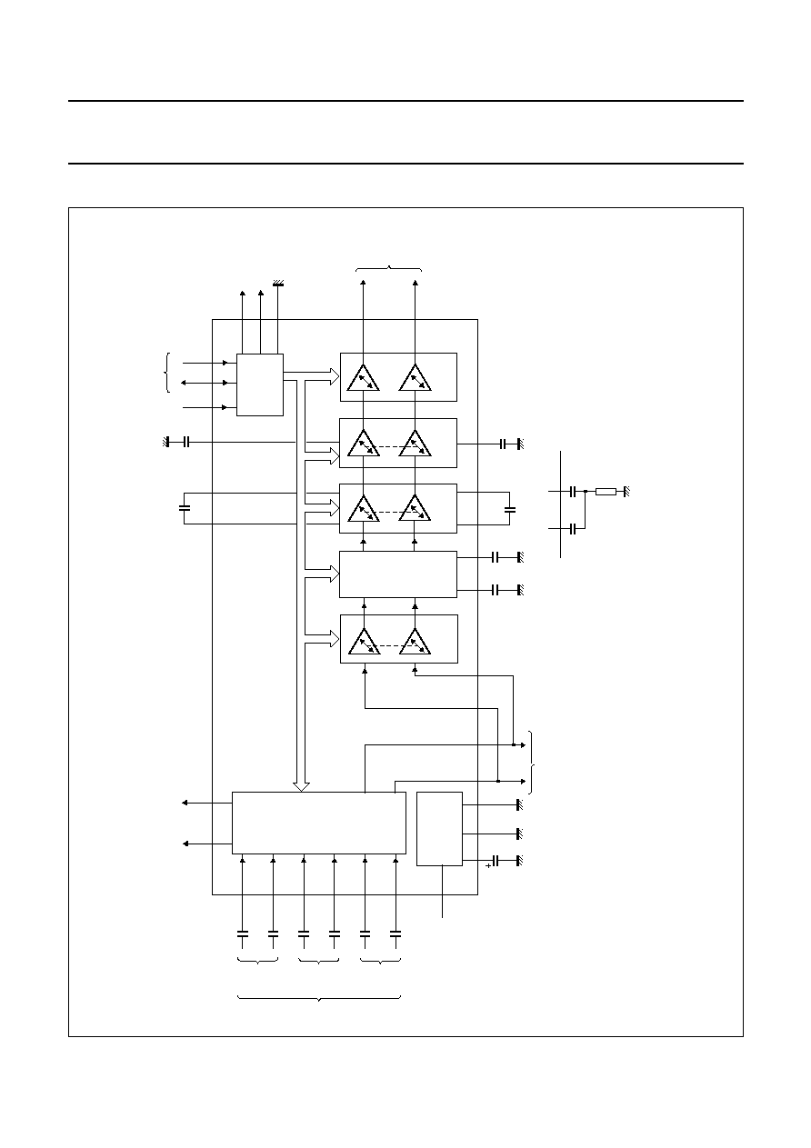
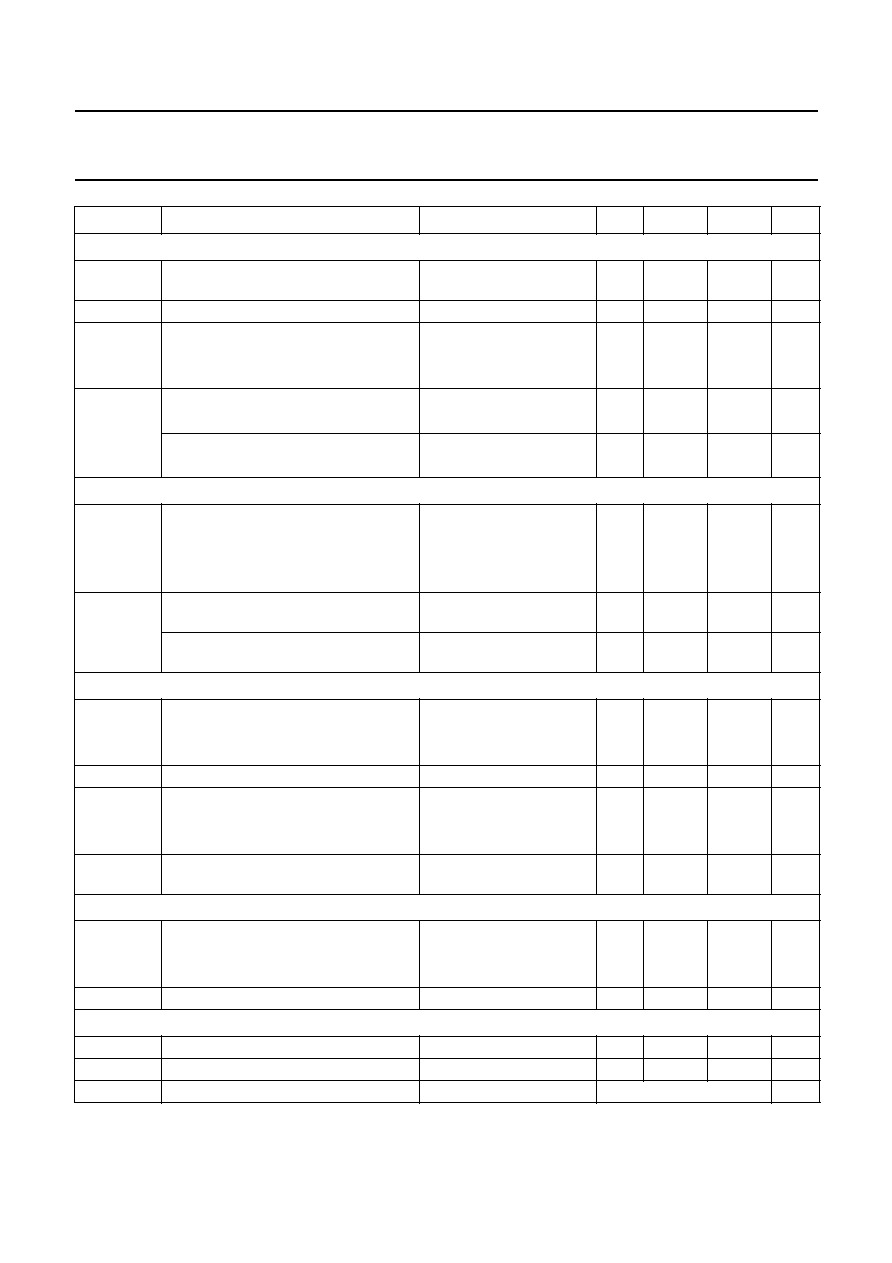
BLOCK DIA
GRAM
f
ull pagewidth
L
470 nF
28 (43)
R
470 nF
30 (3)
L
470 nF
1 (7)
R
470 nF
32 (5)
L
470 nF
3 (9)
R
470 nF
5 (13)
MULTIPLE
SOURCE
AND MODE
SELECTOR
(CROSSBAR
SWITCH)
REFERENCE
VOLTAGE
L
R
VP
+
8 V
6 (14)
SCART
output
L
R
SCOUTL SCOUTR
26 (41)
7 (15)
4 (10)
CSMO
100
µ
F
8
GND
24 (38)
9 (18)
MOUTL MOUTR
LINE output or optional
surround sound decoder
connection
VOLUME
CONTROL
23 (37) 10 (19)
STEREO
MHB917
SPATIAL
STEREO
PSEUDO
STEREO
FORCED
MONO
CPS1 CPS2
29 (2)
27 (42)
BASS
CONTROL
CBR1 CBR2
11 (20) 12 (21)
33 nF
CBL1
CBL2
22 (36) 21 (35)
TREBLE
CONTROL
5.6 nF
CTR
5.6 nF
CTL
14 (25)
VOLUME
BALANCE
MUTE
(30) 18
(26) 15
loudspeaker
channel
outputs
L
R
LOUTR
LOUTL
I
2
C-BUS
INTERFACE
MAD SDA SCL
I
2
C-bus
19 (31)
25
(40)
17
(29)
16 (27)
P2
(4) 31
(17)
TDA9859
(TDA9859H)
11 (22)
12 (21)
68 nF
0.15
µ
F
13 k
extended bass control
(1)
AUX
SCART
MAIN
33 nF
AIN L
AINR
SCIN L
SCIN R
MIN L
MIN R
LINL
LINR
audio
inputs
(1)
(1)
(16)
AGND
P1
(8) 2
DGND
Fig.1 Block diagram and application circuit.
The pin numbers given in parenthesis refer to the TDA9859H version.
(1) For extended bass control, the capacitor between C
BR/L1
and C
BR/L2
should be replaced by the extended bass control network.
2001 Jul 11
4
Philips Semiconductors
Product specification
Universal hi-fi audio processor for TV
TDA9859
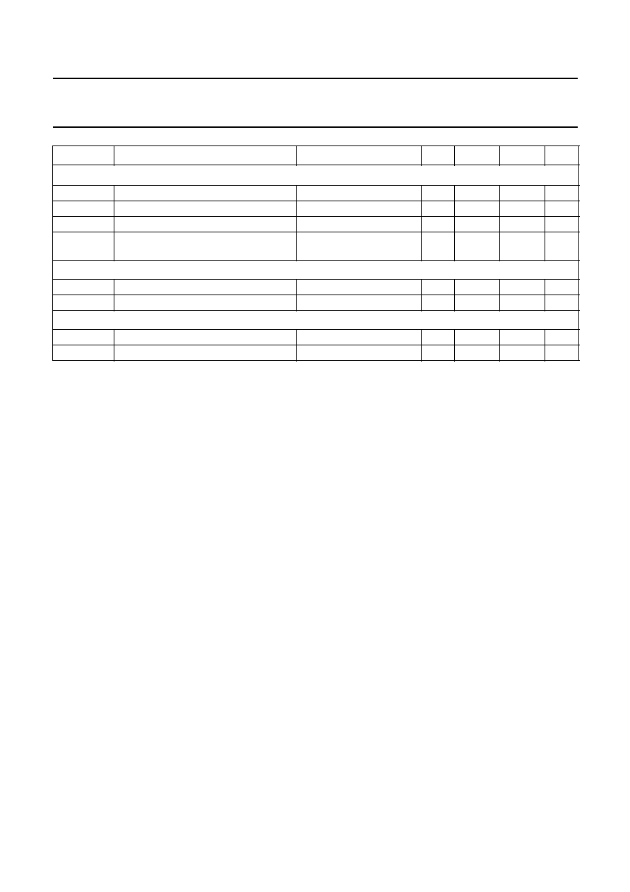
PINNING
SYMBOL
PIN
DESCRIPTION
TDA9859 TDA9859H
SCIN
L
1
7
SCART input;
left channel
P1
2
8
port 1 output
MIN
L
3
9
MAIN input;
left channel
C
SMO
4
10
smoothing
capacitor of
reference voltage
n.c.
-
11
not connected
n.c.
-
12
not connected
MIN
R
5
13
MAIN input;
right channel
V
P
6
14
supply voltage
SCOUT
R
7
15
SCART output;
right channel
GND
8
-
ground
AGND
-
16
analog ground
DGND
-
17
digital ground
MOUT
R
9
18
MAIN output;
right channel
LIN
R
10
19
input to right
loudspeaker
channel
C
BR1
11
20
bass capacitor
connection 1;
right channel
C
BR2
12
21
bass capacitor
connection 2;
right channel
n.c.
-
22
not connected
n.c.
-
23
not connected
n.c.
13
24
not connected
C
TR
14
25
treble capacitor
connection;
right channel
LOUT
R
15
26
loudspeaker output;
right channel
SCL
16
27
serial clock input;
I
2
C-bus
n.c.
-
28
not connected
SDA
17
29
serial data
input/output;
I
2
C-bus
LOUT
L
18
30
loudspeaker output;
left channel
C
TL
19
31
treble capacitor
connection;
left channel
n.c.
20
32
not connected
n.c.
-
33
not connected
n.c.
-
34
not connected
C
BL2
21
35
bass capacitor
connection 2;
left channel
C
BL1
22
36
bass capacitor
connection 1;
left channel
LIN
L
23
37
input to left
loudspeaker
channel
MOUT
L
24
38
MAIN output;
left channel
n.c.
-
39
not connected
MAD
25
40
module address
select input
SCOUT
L
26
41
SCART output;
left channel
C
PS2
27
42
pseudo stereo
capacitor 2
AIN
L
28
43
AUX input;
left channel
n.c.
-
44
not connected
n.c.
-
1
not connected
C
PS1
29
2
pseudo stereo
capacitor 1
AIN
R
30
3
AUX input;
right channel
P2
31
4
port 2 output
SCIN
R
32
5
SCART input signal
RIGHT
n.c.
-
6
not connected
SYMBOL
PIN
DESCRIPTION
TDA9859 TDA9859H
2001 Jul 11
5
Philips Semiconductors
Product specification
Universal hi-fi audio processor for TV
TDA9859
handbook, halfpage
TDA9859
MHA779
1
2
3
4
5
6
7
8
9
10
11
12
13
14
15
16
32
31
30
29
28
27
26
25
24
23
22
21
20
19
18
17
SCINR
SCINL
P2
P1
AINR
MINL
CPS1
CSMO
AINL
MINR
CPS2
SCOUTL
VP
MAD
MOUTL
SCOUTR
LINL
CBL1
CBL2
n.c.
CTL
LOUTL
SDA
GND
MOUTR
LINR
CTR
CBR1
CBR2
n.c.
LOUTR
SCL
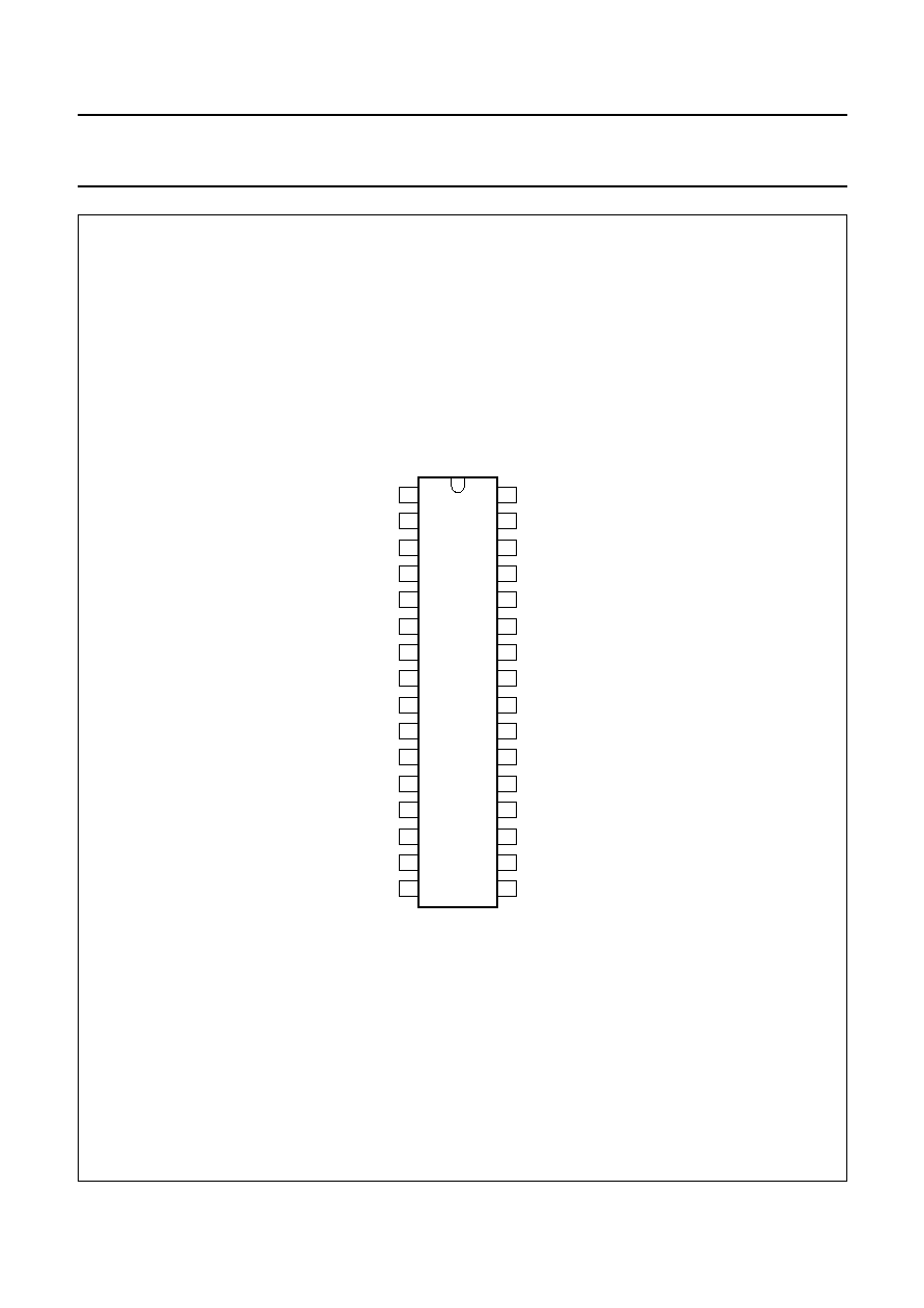
Fig.2 Pin configuration TDA9859 SDIP32 version.
2001 Jul 11
6
Philips Semiconductors
Product specification
Universal hi-fi audio processor for TV
TDA9859
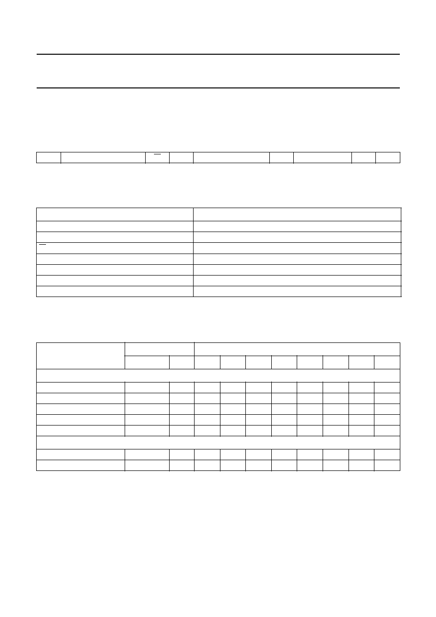
handbook, full pagewidth
TDA9859H
MHB918
1
2
3
4
5
6
7
8
9
10
11
33
32
31
30
29
28
27
26
25
24
23
12
13
14
15
16
17
18
19
20
21
22
44
43
42
41
40
39
38
37
36
35
34
n.c.
AIN
L
C
PS2
SCOUT
L
MAD
n.c.
MOUT
L
LIN
L
C
BL1
C
BL2
n.c.
n.c.
MIN
R
V
P
SCOUT
R
AGND
DGND
MOUT
R
LIN
R
C
BR1
C
BR2
n.c.
n.c.
CPS1
AINR
P2
SCINR
n.c.
SCINL
P1
MINL
CSMO
n.c.
n.c.
n.c.
CTL
LOUTL
SDA
n.c.
SCL
LOUTR
CTR
n.c.
n.c.
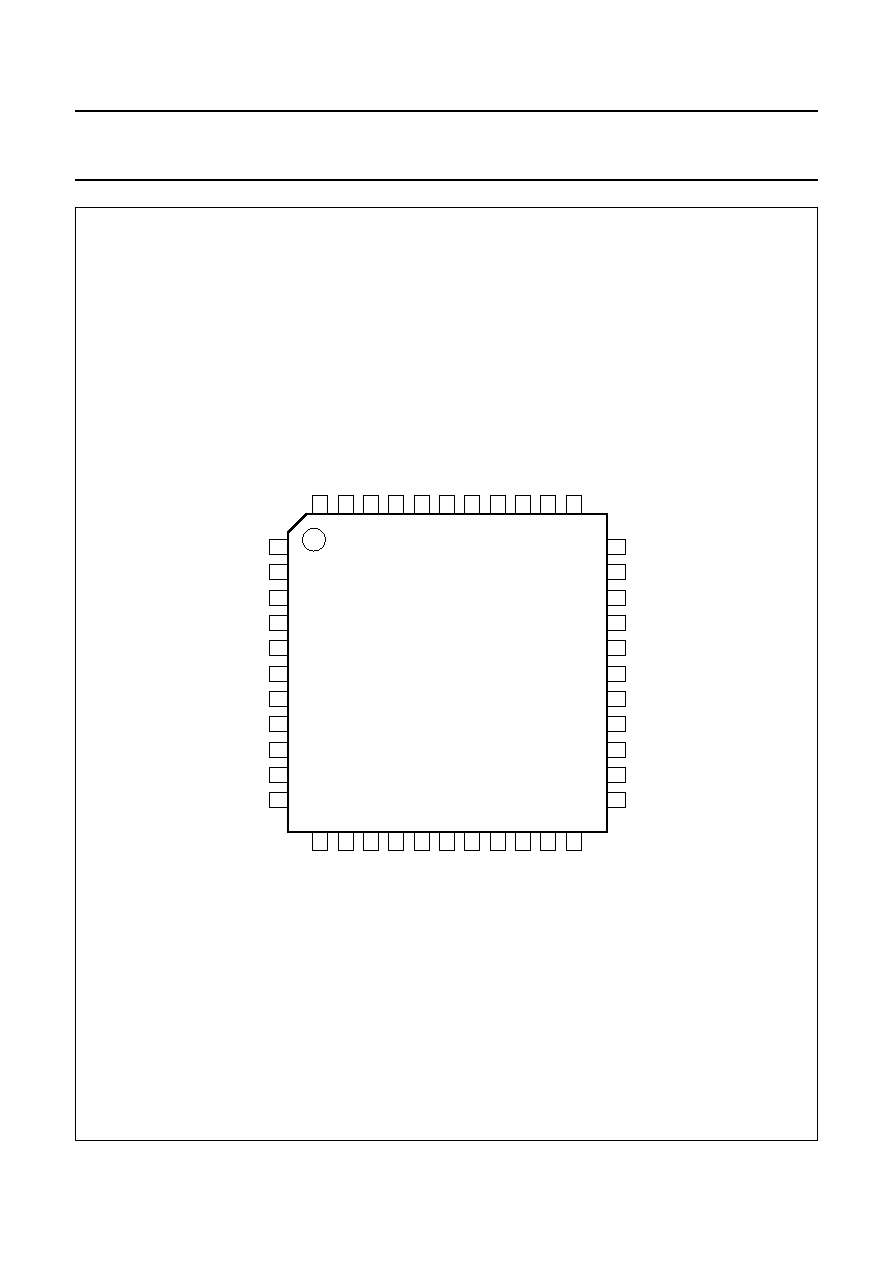
Fig.3 Pin configuration TDA9859H QFP44 version.
2001 Jul 11
7
Philips Semiconductors
Product specification
Universal hi-fi audio processor for TV
TDA9859
FUNCTIONAL DESCRIPTION
The TDA9859 consists of the following functions:
∑
Source select switching block
∑
Loudspeaker channel with effect controls
∑
Two port outputs for general purpose
∑
I
2
C-bus control.
Source select switching block
The TDA9859 selects and switches the input signals from
three stereo or six mono sources MAIN, AUX and SCART
(see Fig.1) to the outputs SCART and loudspeaker
(crossbar-switching; Table 4). The main channel (LINE
outputs) is looped outside the circuit (from pins MOUT
R
and MOUT
L
to pins LIN
R
and LIN
L
), so signals can be
used as LINE output or a surround sound decoder can be
inserted.
Effect controls
`Linear stereo', `stereo with spatial effect (30% or 52%
anti-phase crosstalk)' and `forced mono with or without
pseudo-stereo effect' are controlled by three bits. A muting
of 85 dB is provided.
Loudspeaker channel
Volume control is divided into volume control common and
volume control left/right. The common part
(
-
40 to +15 dB) controls the left and right channels
simultaneously; the left/right part (
-
23 to 0 dB) controls the
volume of left and right channels independently. Treble
control provides a control range from
-
12 to +12 dB and
bass control from
-
12 to +15 dB. Extended bass control
can be provided by an external T-network (see Fig.1) from
-
15 to +19 dB (in 2 dB steps).
I
2
C-bus control
All control settings are stored in subaddress registers.
Data transmission is simplified by auto-incrementing the
subaddresses. The on-chip Power-on reset sets the mute
bit to active, so both the SCART and the loudspeaker
outputs are muted.
The muting can be switched off by writing a `0' (non-muted)
into the mute control bits.
LIMITING VALUES
In accordance with the Absolute Maximum Rating System (IEC 60134).
Notes
1. Equivalent to discharging a 200 pF capacitor through a 0
series resistor (machine model).
2. Equivalent to discharging a 100 pF capacitor through a 1.5 k
series resistor (human body model).
SYMBOL
PARAMETER
CONDITIONS
MIN.
MAX.
UNIT
V
P
supply voltage (pin V
P
)
-
0
10
V
V
n
voltage on all pins, ground excluded
-
0
V
P
V
I
O
output current
at LOUT and SCOUT pins
-
-
2.5
mA
at port output pins
-
-
1.5
mA
P
tot
total power dissipation
-
-
850
mW
T
amb
ambient temperature
-
0
70
∞
C
T
stg
storage temperature
-
-
25
+150
∞
C
V
es
electrostatic handling voltage
all pins; note 1
-
±
300
V
all pins; note 2
-
±
2000
V
2001 Jul 11
8
Philips Semiconductors
Product specification
Universal hi-fi audio processor for TV
TDA9859
THERMAL CHARACTERISTICS
CHARACTERISTICS
V
P
= 8 V; T
amb
= 25
∞
C; treble and bass in linear positions (0 dB); volume control left/right 0 dB; spatial function,
pseudo-stereo function and forced-mono function in off position and measurements taken in Fig.1; unless otherwise
specified.
SYMBOL
PARAMETER
CONDITIONS
VALUE
UNIT
R
th(j-a)
thermal resistance from junction to ambient
in free air
TDA9859 (SDIP32)
60
K/W
TDA9859H (QFP44)
65
K/W
SYMBOL
PARAMETER
CONDITIONS
MIN.
TYP.
MAX.
UNIT
V
P
supply voltage (pin V
P
)
7.2
8.0
8.8
V
I
P
supply current (pin V
P
)
-
25
-
mA
V
ref
internal reference voltage
-
0.5V
P
-
V
V
SMO
voltage at pin C
SMO
-
V
P
-
0.1
-
V
DC voltage on pins
V
I
DC input voltage at pins SCIN, MIN,
LIN and AIN
-
0.5V
P
-
V
V
O
DC output voltage at pins SCOUT,
MOUT and LOUT
-
0.5V
P
-
V
V
C
DC voltage on capacitors (pins C
BR1
,
C
BR2
, C
TR
, C
TL
, C
BL2
, C
BL1
, C
PS2
and C
PS1
)
-
0.5V
P
-
V
Audio select switch; line and SCART outputs (controlled via I
2
C-bus); see Table 4
V
i(rms)
maximum AF input signal on
pins SCIN, MIN and AIN (RMS value)
THD
0.5% on output
pins
2
-
-
V
R
i
input resistance at pins SCIN, MIN and
AIN
20
30
40
k
B
-
0.5 dB
-
0.5 dB bandwidth for pins SCOUT,
MOUT and LOUT
20
-
20 000
Hz
V
o(rms)
maximum AF output signal on
pins SCOUT and MOUT (RMS value)
THD
0.5%
2
-
-
V
R
L
allowed external load resistance
on output pins MOUT
10
-
-
k
on output pins SCOUT
5
-
-
k
G
v
voltage gain from any input to SCART
and MAIN outputs
-
0
-
dB
cr
switch crosstalk on outputs between
AF inputs
f = 10 kHz; unused inputs
connected to ground
-
90
-
dB
2001 Jul 11
9
Philips Semiconductors
Product specification
Universal hi-fi audio processor for TV
TDA9859
Volume control common (f = 1 kHz, 55 steps)
V
i(rms)
maximum input signal on pins LIN
(RMS value)
G
v
= 0; THD
0.5% on
output pins LOUT
2
-
-
V
R
i
input resistance on pins LIN
7.5
10
-
k
G
v
volume control common voltage gain
nominal
-
40
-
+15
dB
minimum
-
38
-
+14
dB
G
v
volume control common voltage
gain step width
G
v
=
-
32 to +15 dB
0.5
1.0
1.5
dB
G
v
=
-
40 to
-
33 dB
0.25
1.0
1.75
dB
volume control common voltage
gain set error
G
v
=
-
32 to +15 dB
-
-
1
dB
G
v
=
-
40 to
-
33 dB
-
-
2
dB
Volume control left/right (f = 1 kHz, 24 steps)
G
v
volume control left/right voltage gain
nominal
-
24
-
0
dB
minimum
-
23
-
-
1
dB
mute position
-
80
-
85
-
dB
G
v
volume control left/right voltage
gain step width
0.5
1.0
1.5
dB
volume control left/right voltage
gain tracking error
-
-
2
dB
Bass control
G
v
bass control voltage gain
C
B
= 33 nF; f = 40 Hz
maximum boost
14
15
16
dB
maximum attenuation
11
12
13
dB
G
v
bass control voltage gain step width
1
1.5
2
dB
G
v(extended)
extended bass control voltage gain
see Fig.1; f = 60 Hz
maximum boost
18
19
20
dB
maximum attenuation
14
15
16
dB
G
v(extended)
extended bass control voltage gain step
width
1
2
3
dB
Treble control
G
v
treble control voltage gain
f = 15 kHz
maximum boost
11
12
13
dB
maximum attenuation
11
12
13
dB
G
v
treble control voltage gain step width
2.5
3
3.5
dB
Effect controls
ct(spat1)
anti-phase crosstalk by spatial effect 1
-
52
-
%
ct(spat2)
anti-phase crosstalk by spatial effect 2
-
30
-
%
phase shift by pseudo-stereo
see Fig.4
SYMBOL
PARAMETER
CONDITIONS
MIN.
TYP.
MAX.
UNIT

2001 Jul 11
10
Philips Semiconductors
Product specification
Universal hi-fi audio processor for TV
TDA9859
Loudspeaker channel outputs (pins LOUT
R
and LOUT
L
)
V
o(max)(rms)
maximum output signal (RMS value)
THD
0.5%; R
L
> 10 k
;
C
L
< 1.5 nF
2
-
-
V
V
DC(max)
maximum DC offset voltage between
adjoining step and any step to mute
for volume control
G
v
= 0 to +15 dB/mute
-
2
15
mV
G
v
=
-
64 to 0 dB/mute
-
0.5
10
mV
for bass control
G
v
= 0 to +15 dB/mute
-
2
15
mV
G
v
=
-
12 to 0 dB/mute
-
0.5
10
mV
for treble control
G
v
=
-
12 to +12 dB/mute
-
0.5
10
mV
R
o
output resistance
-
-
100
R
o(L)
allowed output load resistor
10
-
-
k
C
o(L)
allowed output load capacitor
-
-
1.5
nF
V
no(W)
weighted noise voltage at output
(quasi-peak level)
CCIR 468-3 weighted
G
v
= +15 dB
-
102
-
µ
V
G
v
= 0 dB
-
32
-
µ
V
G
v
=
-
40 dB
-
27
-
µ
V
G
v
=
-
80 dB (mute)
-
20
-
µ
V
B
-
1 dB
-
1 dB bandwidth for loudspeaker
channel
20
-
20000
Hz
THD
total harmonic distortion
f = 20 to 12500 Hz
for V
i(rms)
= 0.2 V
G
v
=
-
30 to +15 dB
-
0.1
0.3
%
for V
i(rms)
= 1 V
G
v
=
-
30 to 0 dB
-
0.1
0.3
%
for V
i(rms)
= 2 V
G
v
=
-
30 to
-
6 dB
-
0.1
0.3
%
cs(l-r)
stereo channel separation
f = 10 kHz; G
v
= 0 dB;
opposite input grounded
by 1 k
resistor
-
75
-
dB
ct(bus)
crosstalk from I
2
C-bus to AF outputs
(V
bus
= spurious I
2
C-bus signal voltage
on AF output)
G
v
= 0 dB
-
100
-
dB
PSRR
100
power supply ripple rejection with
100 Hz ripple
G
v
= 0 dB;
V
ripple(rms)
< 200 mV
-
55
-
dB
SCART output (pins SCOUT
R
and SCOUT
L
)
V
o(max)(rms)
maximum output signal (RMS value)
THD
0.5%; R
L
> 5 k
2
-
-
V
R
o(L)
output load resistor
5
-
-
k
Power-on reset
V
PONR
increasing supply voltage
start of reset
-
-
2.5
V
end of reset
5.2
6.0
6.8
V
decreasing supply voltage
start of reset
4.4
5.2
6.0
V
SYMBOL
PARAMETER
CONDITIONS
MIN.
TYP.
MAX.
UNIT
bus
20 log
V
bus(p-p)
V
o(rms)
---------------------
=
2001 Jul 11
11
Philips Semiconductors
Product specification
Universal hi-fi audio processor for TV
TDA9859
I
2
C-bus (pins SCL and SDA)
V
IH
HIGH-level input voltage
3
-
V
P
V
V
IL
LOW-level input voltage
0
-
1.5
V
I
I
input current
-
-
±
10
µ
A
V
ACK
output voltage with acknowledge at
pin SDA
I
SDA
=
-
3 mA
-
-
0.4
V
Module address (pin MAD)
V
IL
LOW-level input voltage
0
-
1.5
V
V
IH
HIGH-level input voltage
3
-
V
P
V
Port outputs (open-collector outputs pins P1 and P2)
V
OL
LOW-level output voltage
I
O(sink)
= 1 mA
-
-
0.3
V
I
O(sink)
port output sink current
-
-
1
mA
SYMBOL
PARAMETER
CONDITIONS
MIN.
TYP.
MAX.
UNIT
2001 Jul 11
12
Philips Semiconductors
Product specification
Universal hi-fi audio processor for TV
TDA9859
I
2
C-BUS PROTOCOL
This circuit operates as a slave receiver only. For more information about the I
2
C-bus, see
"The I
2
C-bus and how to use
it", order number 9398 393 40011.
I
2
C-bus format
Note
1. Multiple DATA-A (acknowledge) sequences may occur.
Table 1
Explanation of I
2
C-bus format
Note
1. If more than 1 byte of DATA is transmitted, then auto-increment of the subaddress is performed by the device.
Table 2
I
2
C-bus transmission
Note
1. If auto-increment of the subaddress is used, it is necessary to insert three dummy data words between the treble
control byte and the switching control bytes.
S
SLAVE ADDRESS
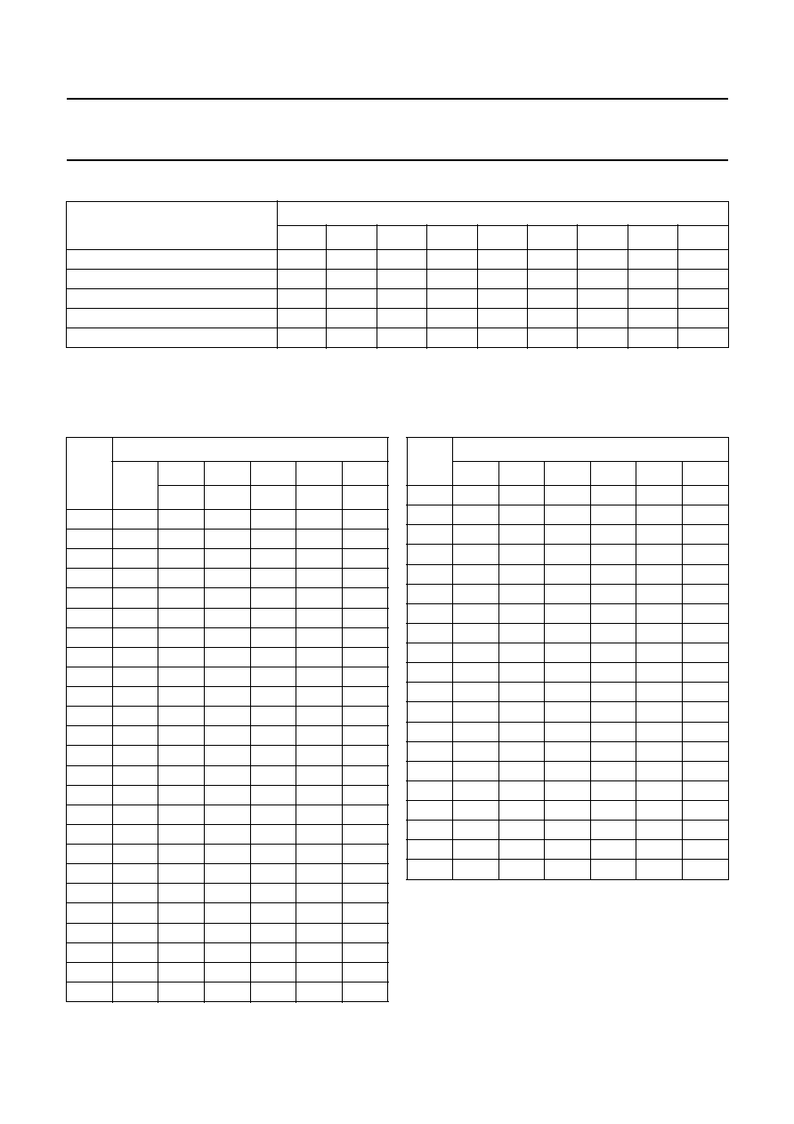
W
A
SUBADDRESS
A
DATA
(1)
A
(1)
P
NAME
DESCRIPTION
S
START condition (SCL HIGH, SDA HIGH-to-LOW)
SLAVE ADDRESS
100 0000 (MAD = LOW) or 100 0001 (MAD = HIGH)
W
0
A
acknowledge (SDA = LOW); generated by the device
SUBADDRESS
subaddress (byte); see Table 2
DATA
(1)
data byte; see Table 2
P
STOP condition (SCL = HIGH, SDA = LOW-to-HIGH)
FUNCTION
SUBADDRESS
DATA BITS
BINARY
HEX
D7
D6
D5
D4
D3
D2
D1
D0
Loudspeaker channel
Volume control common
0000 0000
00
0
0
V05
V04
V03
V02
V01
V00
Volume control left
0000 0001
01
0
0
0
VL4
VL3
VL2
VL1
VL0
Volume control right
0000 0010
02
0
0
0
VR4
VR3
VR2
VR1
VR0
Bass control
0000 0011
03
0
0
0
BA4
BA3
BA2
BA1
BA0
Treble control
0000 0100
04
0
0
0
0
TR3
TR2
TR1
TR0
Switching control byte
SCART output
(1)
0000 1000
08
0
MU1
P1
P2
I13
I12
I11
I10
Loudspeaker output
0000 1001
09
EF2
MU2
EF1
ST
I23
I22
I21
I20
2001 Jul 11
13
Philips Semiconductors
Product specification
Universal hi-fi audio processor for TV
TDA9859
Table 3
Function of the bits in Table 2
Table 4
Input selection
Note
1. Byte 8 (SCART channels): The value of X depends on MU1 and control bits P1 and P2.
Byte 9 (loudspeaker channels): see Table 5 for the programming of these bits. The value of X depends on the
selected effects and MU2.
BITS
FUNCTION
V00 to V05
volume control common for loudspeaker channel; see Table 9
VL0 to VL4
volume control for left loudspeaker channel; see Table 6
VR0 to VR4
volume control for right loudspeaker channel; see Table 6
BA0 to BA4
bass control for left and right loudspeaker channels; see Table 7
TR0 to TR3
treble control for left and right loudspeaker channels; see Table 8
I10 to I13
input selection for SCART channels; see Table 4
I20 to I23
input selection for loudspeaker channels; see Table 4
MU1 and MU2
mute control bits (MU1 for SCART channel, MU2 for loudspeaker channel)
0 = channel not muted
1 = channel muted
EF1, EF2 and ST
effect control bits for loudspeaker channel; see Table 5
P1 and P2
control bits for ports P1 and P2
control bit = 0: port output = LOW-level
control bit = 1: port output = HIGH-level
INPUT
BITS OF DATA BYTE 8 AND 9
HEX
D7
D6
D5
D4
D3
D2
D1
D0
AUX LEFT
XB
(1)
(1)
MU
(1)
(1)
1
0
1
1
AUX RIGHT
X9
(1)
(1)
MU
(1)
(1)
1
0
0
1
AUX STEREO
X7
(1)
(1)
MU
(1)
(1)
0
1
1
1
SCART LEFT
XA
(1)
(1)
MU
(1)
(1)
1
0
1
0
SCART RIGHT
X5
(1)
(1)
MU
(1)
(1)
0
1
0
1
SCART STEREO
X6
(1)
(1)
MU
(1)
(1)
0
1
1
0
MAIN LEFT
XC
(1)
(1)
MU
(1)
(1)
1
1
0
0
MAIN RIGHT
XD
(1)
(1)
MU
(1)
(1)
1
1
0
1
MAIN STEREO
X8
(1)
(1)
MU
(1)
(1)
1
0
0
0
2001 Jul 11
14
Philips Semiconductors
Product specification
Universal hi-fi audio processor for TV
TDA9859
Table 5
Effect controls
Note
1. The value of X depends on the selected input (see Table 4).
SETTING SPECIAL EFFECTS
DATA BYTE TO SUBADDRESS 09
HEX
EF2
MU2
EF1
ST
I23
I22
I21
I20
Stereo with spatial effect 1 (52%)
BX
(1)
1
0
1
1
(1)
(1)
(1)
(1)
Stereo with spatial effect 2 (30%)
3X
(1)
0
0
1
1
(1)
(1)
(1)
(1)
Stereo without spatial effect
1X
(1)
0
0
0
1
(1)
(1)
(1)
(1)
Forced mono with pseudo stereo
2X
(1)
0
0
1
0
(1)
(1)
(1)
(1)
Forced mono without pseudo stereo
0X
(1)
0
0
0
0
(1)
(1)
(1)
(1)
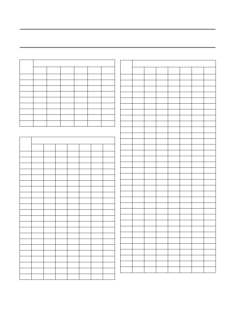
Table 6
Volume control left/right
Table 7
Bass control
G
v
(dB)
DATA BITS
HEX
VL4
VL3
VL2
VL1
VL0
VR4
VR3
VR2
VR1
VR0
0
1F
1
1
1
1
1
-
1
1E
1
1
1
1
0
-
2
1D
1
1
1
0
1
-
3
1C
1
1
1
0
0
-
4
1B
1
1
0
1
1
-
5
1A
1
1
0
1
0
-
6
19
1
1
0
0
1
-
7
18
1
1
0
0
0
-
8
17
1
0
1
1
1
-
9
16
1
0
1
1
0
-
10
15
1
0
1
0
1
-
11
14
1
0
1
0
0
-
12
13
1
0
0
1
1
-
13
12
1
0
0
1
0
-
14
11
1
0
0
0
1
-
15
10
1
0
0
0
0
-
16
0F
0
1
1
1
1
-
17
0E
0
1
1
1
0
-
18
0D
0
1
1
0
1
-
19
0C
0
1
1
0
0
-
20
0B
0
1
0
1
1
-
21
0A
0
1
0
1
0
-
22
09
0
1
0
0
1
-
23
08
0
1
0
0
0
Mute
07
0
0
1
1
1
G
v
(dB)
DATA BITS
HEX
BA4
BA3
BA2
BA1
BA0
+15
19
1
1
0
0
1
+13.5
18
1
1
0
0
0
+12
17
1
0
1
1
1
+10.5
16
1
0
1
1
0
+9
15
1
0
1
0
1
+7.5
14
1
0
1
0
0
+6
13
1
0
0
1
1
+4.5
12
1
0
0
1
0
+3
11
1
0
0
0
1
+1.5
10
1
0
0
0
0
0
0F
0
1
1
1
1
0
0E
0
1
1
1
0
-
1.5
0D
0
1
1
0
1
-
3
0C
0
1
1
0
0
-
4.5
0B
0
1
0
1
1
-
6
0A
0
1
0
1
0
-
7.5
09
0
1
0
0
1
-
9
08
0
1
0
0
0
-
10.5
07
0
0
1
1
1
-
12
06
0
0
1
1
0
2001 Jul 11
15
Philips Semiconductors
Product specification
Universal hi-fi audio processor for TV
TDA9859
Table 8
Treble control
Table 9
Volume control common
G
v
(dB)
DATA BITS
HEX
0
TR3
TR2
TR1
TR0
+12
0A
0
1
0
1
0
+9
09
0
1
0
0
1
+6
08
0
1
0
0
0
+3
07
0
0
1
1
1
0
06
0
0
1
1
0
-
3
05
0
0
1
0
1
-
6
04
0
0
1
0
0
-
9
03
0
0
0
1
1
-
12
02
0
0
0
1
0
G
v
(dB)
DATA BITS
HEX
V05
V04
V03
V02
V01
V00
+15
3F
1
1
1
1
1
1
+14
3E
1
1
1
1
1
0
+13
3D
1
1
1
1
0
1
+12
3C
1
1
1
1
0
0
+11
3B
1
1
1
0
1
1
+10
3A
1
1
1
0
1
0
+9
39
1
1
1
0
0
1
+8
38
1
1
1
0
0
0
+7
37
1
1
0
1
1
1
+6
36
1
1
0
1
1
0
+5
35
1
1
0
1
0
1
+4
34
1
1
0
1
0
0
+3
33
1
1
0
0
1
1
+2
32
1
1
0
0
1
0
+1
31
1
1
0
0
0
1
0
30
1
1
0
0
0
0
-
1
2F
1
0
1
1
1
1
-
2
2E
1
0
1
1
1
0
-
3
2D
1
0
1
1
0
1
-
4
2C
1
0
1
1
0
0
-
5
2B
1
0
1
0
1
1
-
6
2A
1
0
1
0
1
0
-
7
29
1
0
1
0
0
1
-
8
28
1
0
1
0
0
0
-
9
27
1
0
0
1
1
1
-
10
26
1
0
0
1
1
0
-
11
25
1
0
0
1
0
1
-
12
24
1
0
0
1
0
0
-
13
23
1
0
0
0
1
1
-
14
22
1
0
0
0
1
0
-
15
21
1
0
0
0
0
1
-
16
20
1
0
0
0
0
0
-
17
1F
0
1
1
1
1
1
-
18
1E
0
1
1
1
1
0
-
19
1D
0
1
1
1
0
1
-
20
1C
0
1
1
1
0
0
-
21
1B
0
1
1
0
1
1
-
22
1A
0
1
1
0
1
0
-
23
19
0
1
1
0
0
1
-
24
18
0
1
1
0
0
0
-
25
17
0
1
0
1
1
1
-
26
16
0
1
0
1
1
0
-
27
15
0
1
0
1
0
1
-
28
14
0
1
0
1
0
0
-
29
13
0
1
0
0
1
1
-
30
12
0
1
0
0
1
0
-
31
11
0
1
0
0
0
1
-
32
10
0
1
0
0
0
0
-
33
0F
0
0
1
1
1
1
-
34
0E
0
0
1
1
1
0
-
35
0D
0
0
1
1
0
1
-
36
0C
0
0
1
1
0
0
-
37
0B
0
0
1
0
1
1
-
38
0A
0
0
1
0
1
0
-
39
09
0
0
1
0
0
1
-
40
08
0
0
1
0
0
0
G
v
(dB)
DATA BITS
HEX
V05
V04
V03
V02
V01
V00
2001 Jul 11
16
Philips Semiconductors
Product specification
Universal hi-fi audio processor for TV
TDA9859
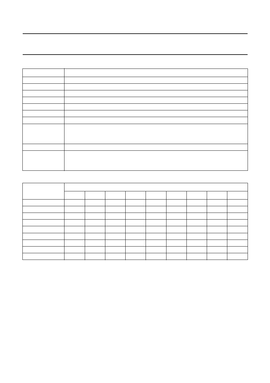
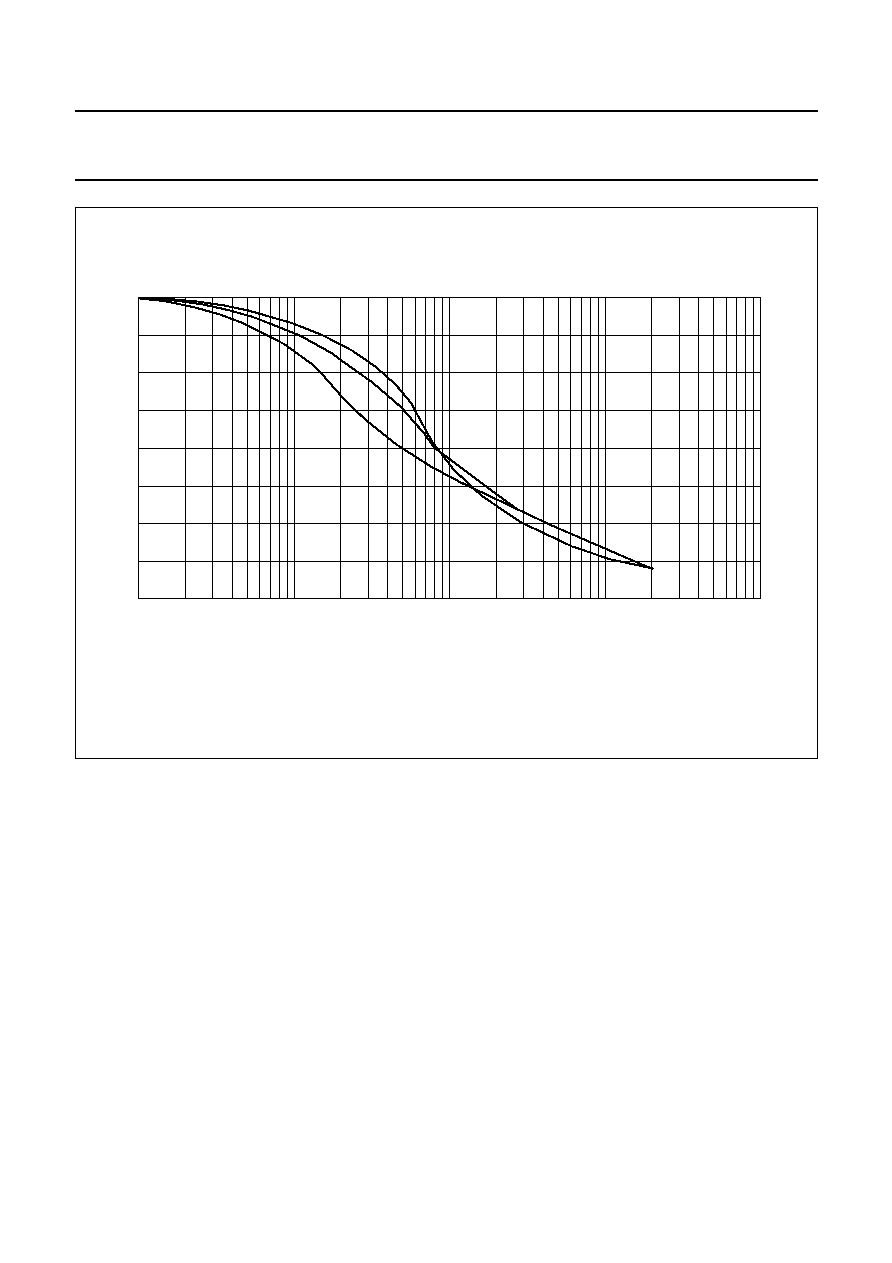
handbook, full pagewidth
-
400
0
(1)
(2)
(3)
phase
(degree)
-
300
-
200
-
100
MHA311
10
2
10
3
10
4
f (Hz)
10
5
10
Fig.4 Pseudo stereo effect (phase) as a function of frequency.
(1) Normal effect; C
PS1
= C
PS2
= 15 nF.
(2) Intensified effect; C
PS1
= 47 nF; C
PS2
= 5.6 nF.
(3) More intensified effect; C
PS1
= 68 nF; C
PS2
= 5.6 nF.
2001 Jul 11
17
Philips Semiconductors
Product specification
Universal hi-fi audio processor for TV
TDA9859
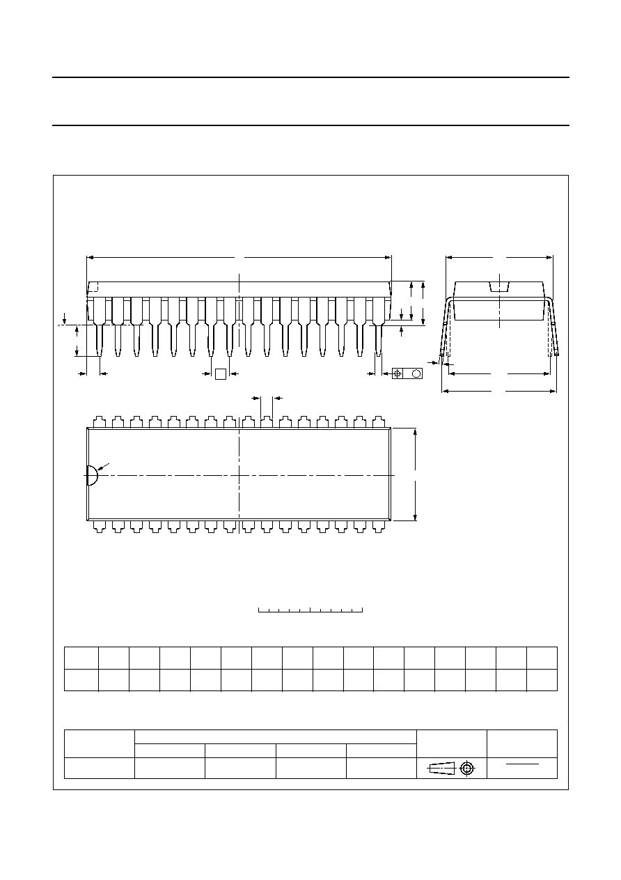
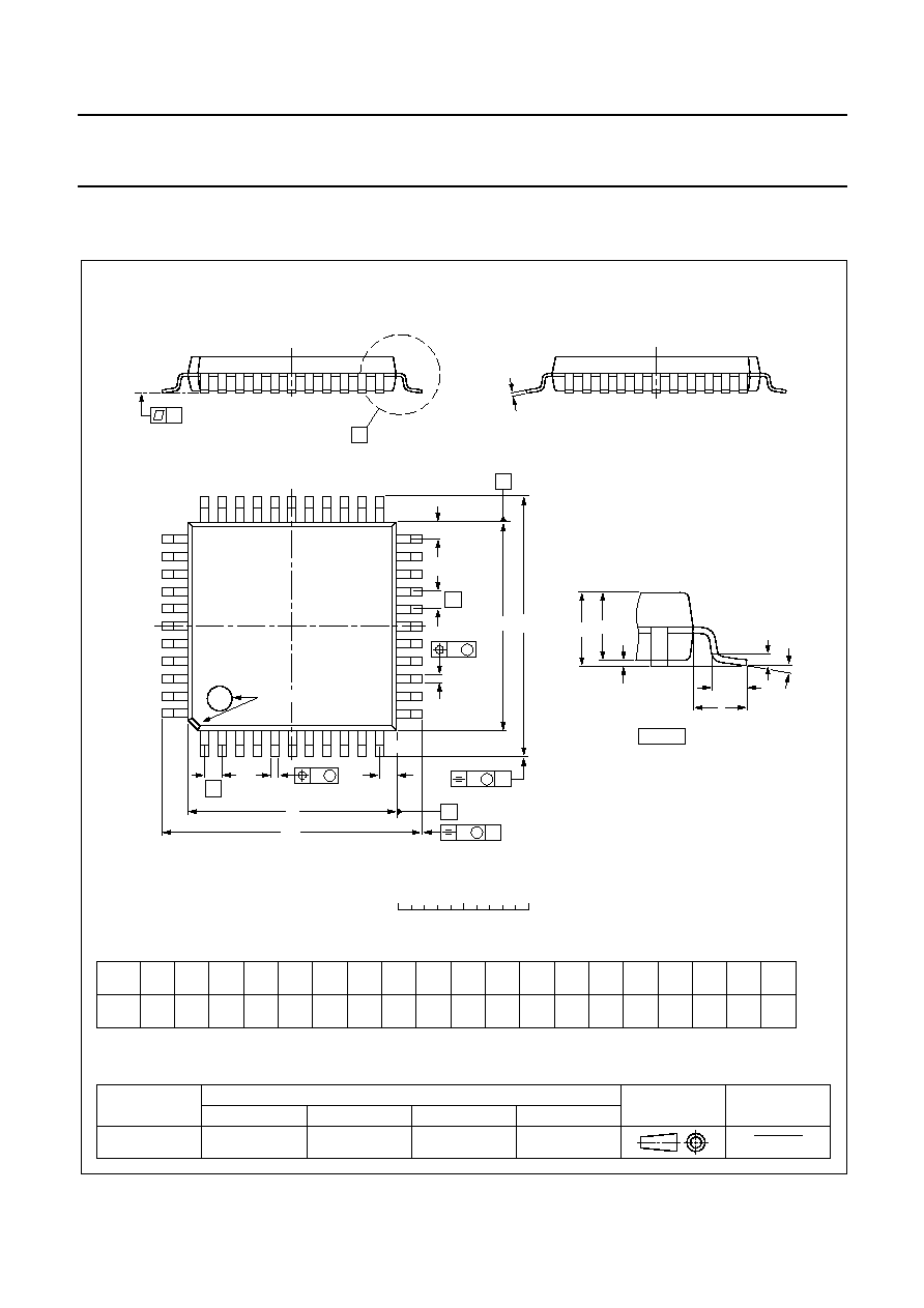
PACKAGE OUTLINES
UNIT
b
1
c
E
e
M
H
L
REFERENCES
OUTLINE
VERSION
EUROPEAN
PROJECTION
ISSUE DATE
IEC
JEDEC
EIAJ
mm
DIMENSIONS (mm are the original dimensions)
SOT232-1
92-11-17
95-02-04
b
max.
w
M
E
e
1
1.3
0.8
0.53
0.40
0.32
0.23
29.4
28.5
9.1
8.7
3.2
2.8
0.18
1.778
10.16
10.7
10.2
12.2
10.5
1.6
4.7
0.51
3.8
M
H
c
(e )
1
M
E
A
L
seating plane
A
1
w
M
b
1
e
D
A
2
Z
32
1
17
16
b
E
pin 1 index
0
5
10 mm
scale
Note
1. Plastic or metal protrusions of 0.25 mm maximum per side are not included.
(1)
(1)
D
(1)
Z
A
max.
1
2
A
min.
A
max.
SDIP32: plastic shrink dual in-line package; 32 leads (400 mil)
SOT232-1
2001 Jul 11
18
Philips Semiconductors
Product specification
Universal hi-fi audio processor for TV
TDA9859
UNIT
A
1
A
2
A
3
b
p
c
E
(1)
e
H
E
L
L
p
Z
y
w
v
REFERENCES
OUTLINE
VERSION
EUROPEAN
PROJECTION
ISSUE DATE
IEC
JEDEC
EIAJ
mm
0.25
0.05
1.85
1.65
0.25
0.40
0.20
0.25
0.14
10.1
9.9
0.8
1.3
12.9
12.3
1.2
0.8
10
0
o
o
0.15
0.1
0.15
DIMENSIONS (mm are the original dimensions)
Note
1. Plastic or metal protrusions of 0.25 mm maximum per side are not included.
0.95
0.55
SOT307-2
95-02-04
97-08-01
D
(1)
(1)
(1)
10.1
9.9
H
D
12.9
12.3
E
Z
1.2
0.8
D
e
E
B
11
c
E
H
D
ZD
A
Z E
e
v
M
A
X
1
44
34
33
23
22
12
y
A
1
A
L
p
detail X
L
(A )
3
A
2
pin 1 index
D
H
v
M
B
b
p
b
p
w
M
w
M
0
2.5
5 mm
scale
QFP44: plastic quad flat package; 44 leads (lead length 1.3 mm); body 10 x 10 x 1.75 mm
SOT307-2
A
max.
2.10

2001 Jul 11
19
Philips Semiconductors
Product specification
Universal hi-fi audio processor for TV
TDA9859
SOLDERING
Introduction
This text gives a very brief insight to a complex technology.
A more in-depth account of soldering ICs can be found in
our
"Data Handbook IC26; Integrated Circuit Packages"
(document order number 9398 652 90011).
There is no soldering method that is ideal for all IC
packages. Wave soldering is often preferred when
through-hole and surface mount components are mixed on
one printed-circuit board. Wave soldering can still be used
for certain surface mount ICs, but it is not suitable for fine
pitch SMDs. In these situations reflow soldering is
recommended.
Through-hole mount packages
S
OLDERING BY DIPPING OR BY SOLDER WAVE
The maximum permissible temperature of the solder is
260
∞
C; solder at this temperature must not be in contact
with the joints for more than 5 seconds. The total contact
time of successive solder waves must not exceed
5 seconds.
The device may be mounted up to the seating plane, but
the temperature of the plastic body must not exceed the
specified maximum storage temperature (T
stg(max)
). If the
printed-circuit board has been pre-heated, forced cooling
may be necessary immediately after soldering to keep the
temperature within the permissible limit.
M
ANUAL SOLDERING
Apply the soldering iron (24 V or less) to the lead(s) of the
package, either below the seating plane or not more than
2 mm above it. If the temperature of the soldering iron bit
is less than 300
∞
C it may remain in contact for up to
10 seconds. If the bit temperature is between
300 and 400
∞
C, contact may be up to 5 seconds.
Surface mount packages
R
EFLOW SOLDERING
Reflow soldering requires solder paste (a suspension of
fine solder particles, flux and binding agent) to be applied
to the printed-circuit board by screen printing, stencilling or
pressure-syringe dispensing before package placement.
Several methods exist for reflowing; for example,
convection or convection/infrared heating in a conveyor
type oven. Throughput times (preheating, soldering and
cooling) vary between 100 and 200 seconds depending
on heating method.
Typical reflow peak temperatures range from
215 to 250
∞
C. The top-surface temperature of the
packages should preferable be kept below 220
∞
C for
thick/large packages, and below 235
∞
C for small/thin
packages.
W
AVE SOLDERING
Conventional single wave soldering is not recommended
for surface mount devices (SMDs) or printed-circuit boards
with a high component density, as solder bridging and
non-wetting can present major problems.
To overcome these problems the double-wave soldering
method was specifically developed.
If wave soldering is used the following conditions must be
observed for optimal results:
∑
Use a double-wave soldering method comprising a
turbulent wave with high upward pressure followed by a
smooth laminar wave.
∑
For packages with leads on two sides and a pitch (e):
≠ larger than or equal to 1.27 mm, the footprint
longitudinal axis is preferred to be parallel to the
transport direction of the printed-circuit board;
≠ smaller than 1.27 mm, the footprint longitudinal axis
must be parallel to the transport direction of the
printed-circuit board.
The footprint must incorporate solder thieves at the
downstream end.
∑
For packages with leads on four sides, the footprint must
be placed at a 45
∞
angle to the transport direction of the
printed-circuit board. The footprint must incorporate
solder thieves downstream and at the side corners.
During placement and before soldering, the package must
be fixed with a droplet of adhesive. The adhesive can be
applied by screen printing, pin transfer or syringe
dispensing. The package can be soldered after the
adhesive is cured.
Typical dwell time is 4 seconds at 250
∞
C.
A mildly-activated flux will eliminate the need for removal
of corrosive residues in most applications.
M
ANUAL SOLDERING
Fix the component by first soldering two
diagonally-opposite end leads. Use a low voltage (24 V or
less) soldering iron applied to the flat part of the lead.
Contact time must be limited to 10 seconds at up to
300
∞
C. When using a dedicated tool, all other leads can
be soldered in one operation within 2 to 5 seconds
between 270 and 320
∞
C.

2001 Jul 11
20
Philips Semiconductors
Product specification
Universal hi-fi audio processor for TV
TDA9859
Suitability of IC packages for wave, reflow and dipping soldering methods
Notes
1. All surface mount (SMD) packages are moisture sensitive. Depending upon the moisture content, the maximum
temperature (with respect to time) and body size of the package, there is a risk that internal or external package
cracks may occur due to vaporization of the moisture in them (the so called popcorn effect). For details, refer to the
Drypack information in the
"Data Handbook IC26; Integrated Circuit Packages; Section: Packing Methods".
2. For SDIP packages, the longitudinal axis must be parallel to the transport direction of the printed-circuit board.
3. These packages are not suitable for wave soldering as a solder joint between the printed-circuit board and heatsink
(at bottom version) can not be achieved, and as solder may stick to the heatsink (on top version).
4. If wave soldering is considered, then the package must be placed at a 45
∞
angle to the solder wave direction.
The package footprint must incorporate solder thieves downstream and at the side corners.
5. Wave soldering is only suitable for LQFP, QFP and TQFP packages with a pitch (e) equal to or larger than 0.8 mm;
it is definitely not suitable for packages with a pitch (e) equal to or smaller than 0.65 mm.
6. Wave soldering is only suitable for SSOP and TSSOP packages with a pitch (e) equal to or larger than 0.65 mm; it is
definitely not suitable for packages with a pitch (e) equal to or smaller than 0.5 mm.
MOUNTING
PACKAGE
SOLDERING METHOD
WAVE
REFLOW
(1)
DIPPING
Through-hole mount DBS, DIP, HDIP, SDIP, SIL
suitable
(2)
-
suitable
Surface mount
BGA, HBGA, LFBGA, SQFP, TFBGA
not suitable
suitable
-
HBCC, HLQFP, HSQFP, HSOP, HTQFP,
HTSSOP, HVQFN, SMS
not suitable
(3)
suitable
-
PLCC
(4)
, SO, SOJ
suitable
suitable
-
LQFP, QFP, TQFP
not recommended
(4)(5)
suitable
-
SSOP, TSSOP, VSO
not recommended
(6)
suitable
-

2001 Jul 11
21
Philips Semiconductors
Product specification
Universal hi-fi audio processor for TV
TDA9859
DATA SHEET STATUS
Notes
1. Please consult the most recently issued data sheet before initiating or completing a design.
2. The product status of the device(s) described in this data sheet may have changed since this data sheet was
published. The latest information is available on the Internet at URL http://www.semiconductors.philips.com.
DATA SHEET STATUS
(1)
PRODUCT
STATUS
(2)
DEFINITIONS
Objective specification
Development
This data sheet contains data from the objective specification for product
development. Philips Semiconductors reserves the right to change the
specification in any manner without notice.
Preliminary specification
Qualification
This data sheet contains data from the preliminary specification.
Supplementary data will be published at a later date. Philips
Semiconductors reserves the right to change the specification without
notice, in order to improve the design and supply the best possible
product.
Product specification
Production
This data sheet contains data from the product specification. Philips
Semiconductors reserves the right to make changes at any time in order
to improve the design, manufacturing and supply. Changes will be
communicated according to the Customer Product/Process Change
Notification (CPCN) procedure SNW-SQ-650A.
DEFINITIONS
Short-form specification
The data in a short-form
specification is extracted from a full data sheet with the
same type number and title. For detailed information see
the relevant data sheet or data handbook.
Limiting values definition
Limiting values given are in
accordance with the Absolute Maximum Rating System
(IEC 60134). Stress above one or more of the limiting
values may cause permanent damage to the device.
These are stress ratings only and operation of the device
at these or at any other conditions above those given in the
Characteristics sections of the specification is not implied.
Exposure to limiting values for extended periods may
affect device reliability.
Application information
Applications that are
described herein for any of these products are for
illustrative purposes only. Philips Semiconductors make
no representation or warranty that such applications will be
suitable for the specified use without further testing or
modification.
DISCLAIMERS
Life support applications
These products are not
designed for use in life support appliances, devices, or
systems where malfunction of these products can
reasonably be expected to result in personal injury. Philips
Semiconductors customers using or selling these products
for use in such applications do so at their own risk and
agree to fully indemnify Philips Semiconductors for any
damages resulting from such application.
Right to make changes
Philips Semiconductors
reserves the right to make changes, without notice, in the
products, including circuits, standard cells, and/or
software, described or contained herein in order to
improve design and/or performance. Philips
Semiconductors assumes no responsibility or liability for
the use of any of these products, conveys no licence or title
under any patent, copyright, or mask work right to these
products, and makes no representations or warranties that
these products are free from patent, copyright, or mask
work right infringement, unless otherwise specified.

2001 Jul 11
22
Philips Semiconductors
Product specification
Universal hi-fi audio processor for TV
TDA9859
PURCHASE OF PHILIPS I
2
C COMPONENTS
Purchase of Philips I
2
C components conveys a license under the Philips' I
2
C patent to use the
components in the I
2
C system provided the system conforms to the I
2
C specification defined by
Philips. This specification can be ordered using the code 9398 393 40011.

2001 Jul 11
23
Philips Semiconductors
Product specification
Universal hi-fi audio processor for TV
TDA9859
NOTES

© Philips Electronics N.V.
SCA
All rights are reserved. Reproduction in whole or in part is prohibited without the prior written consent of the copyright owner.
The information presented in this document does not form part of any quotation or contract, is believed to be accurate and reliable and may be changed
without notice. No liability will be accepted by the publisher for any consequence of its use. Publication thereof does not convey nor imply any license
under patent- or other industrial or intellectual property rights.
Internet: http://www.semiconductors.philips.com
2001
72
Philips Semiconductors ≠ a worldwide company
For all other countries apply to: Philips Semiconductors,
Marketing Communications, Building BE-p, P.O. Box 218, 5600 MD EINDHOVEN,
The Netherlands, Fax. +31 40 27 24825
Argentina: see South America
Australia: 3 Figtree Drive, HOMEBUSH, NSW 2140,
Tel. +61 2 9704 8141, Fax. +61 2 9704 8139
Austria: Computerstr. 6, A-1101 WIEN, P.O. Box 213,
Tel. +43 1 60 101 1248, Fax. +43 1 60 101 1210
Belarus: Hotel Minsk Business Center, Bld. 3, r. 1211, Volodarski Str. 6,
220050 MINSK, Tel. +375 172 20 0733, Fax. +375 172 20 0773
Belgium: see The Netherlands
Brazil: see South America
Bulgaria: Philips Bulgaria Ltd., Energoproject, 15th floor,
51 James Bourchier Blvd., 1407 SOFIA,
Tel. +359 2 68 9211, Fax. +359 2 68 9102
Canada: PHILIPS SEMICONDUCTORS/COMPONENTS,
Tel. +1 800 234 7381, Fax. +1 800 943 0087
China/Hong Kong: 501 Hong Kong Industrial Technology Centre,
72 Tat Chee Avenue, Kowloon Tong, HONG KONG,
Tel. +852 2319 7888, Fax. +852 2319 7700
Colombia: see South America
Czech Republic: see Austria
Denmark: Sydhavnsgade 23, 1780 COPENHAGEN V,
Tel. +45 33 29 3333, Fax. +45 33 29 3905
Finland: Sinikalliontie 3, FIN-02630 ESPOO,
Tel. +358 9 615 800, Fax. +358 9 6158 0920
France: 7 - 9 Rue du Mont ValÈrien, BP317, 92156 SURESNES Cedex,
Tel. +33 1 4728 6600, Fax. +33 1 4728 6638
Germany: Hammerbrookstraþe 69, D-20097 HAMBURG,
Tel. +49 40 2353 60, Fax. +49 40 2353 6300
Hungary: Philips Hungary Ltd., H-1119 Budapest, Fehervari ut 84/A,
Tel: +36 1 382 1700, Fax: +36 1 382 1800
India: Philips INDIA Ltd, Band Box Building, 2nd floor,
254-D, Dr. Annie Besant Road, Worli, MUMBAI 400 025,
Tel. +91 22 493 8541, Fax. +91 22 493 0966
Indonesia: PT Philips Development Corporation, Semiconductors Division,
Gedung Philips, Jl. Buncit Raya Kav.99-100, JAKARTA 12510,
Tel. +62 21 794 0040 ext. 2501, Fax. +62 21 794 0080
Ireland: Newstead, Clonskeagh, DUBLIN 14,
Tel. +353 1 7640 000, Fax. +353 1 7640 200
Israel: RAPAC Electronics, 7 Kehilat Saloniki St, PO Box 18053,
TEL AVIV 61180, Tel. +972 3 645 0444, Fax. +972 3 649 1007
Italy: PHILIPS SEMICONDUCTORS, Via Casati, 23 - 20052 MONZA (MI),
Tel. +39 039 203 6838, Fax +39 039 203 6800
Japan: Philips Bldg 13-37, Kohnan 2-chome, Minato-ku,
TOKYO 108-8507, Tel. +81 3 3740 5130, Fax. +81 3 3740 5057
Korea: Philips House, 260-199 Itaewon-dong, Yongsan-ku, SEOUL,
Tel. +82 2 709 1412, Fax. +82 2 709 1415
Malaysia: No. 76 Jalan Universiti, 46200 PETALING JAYA, SELANGOR,
Tel. +60 3 750 5214, Fax. +60 3 757 4880
Mexico: 5900 Gateway East, Suite 200, EL PASO, TEXAS 79905,
Tel. +9-5 800 234 7381, Fax +9-5 800 943 0087
Middle East: see Italy
Netherlands: Postbus 90050, 5600 PB EINDHOVEN, Bldg. VB,
Tel. +31 40 27 82785, Fax. +31 40 27 88399
New Zealand: 2 Wagener Place, C.P.O. Box 1041, AUCKLAND,
Tel. +64 9 849 4160, Fax. +64 9 849 7811
Norway: Box 1, Manglerud 0612, OSLO,
Tel. +47 22 74 8000, Fax. +47 22 74 8341
Pakistan: see Singapore
Philippines: Philips Semiconductors Philippines Inc.,
106 Valero St. Salcedo Village, P.O. Box 2108 MCC, MAKATI,
Metro MANILA, Tel. +63 2 816 6380, Fax. +63 2 817 3474
Poland: Al.Jerozolimskie 195 B, 02-222 WARSAW,
Tel. +48 22 5710 000, Fax. +48 22 5710 001
Portugal: see Spain
Romania: see Italy
Russia: Philips Russia, Ul. Usatcheva 35A, 119048 MOSCOW,
Tel. +7 095 755 6918, Fax. +7 095 755 6919
Singapore: Lorong 1, Toa Payoh, SINGAPORE 319762,
Tel. +65 350 2538, Fax. +65 251 6500
Slovakia: see Austria
Slovenia: see Italy
South Africa: S.A. PHILIPS Pty Ltd., 195-215 Main Road Martindale,
2092 JOHANNESBURG, P.O. Box 58088 Newville 2114,
Tel. +27 11 471 5401, Fax. +27 11 471 5398
South America: Al. Vicente Pinzon, 173, 6th floor,
04547-130 S√O PAULO, SP, Brazil,
Tel. +55 11 821 2333, Fax. +55 11 821 2382
Spain: Balmes 22, 08007 BARCELONA,
Tel. +34 93 301 6312, Fax. +34 93 301 4107
Sweden: Kottbygatan 7, Akalla, S-16485 STOCKHOLM,
Tel. +46 8 5985 2000, Fax. +46 8 5985 2745
Switzerland: Allmendstrasse 140, CH-8027 ZÐRICH,
Tel. +41 1 488 2741 Fax. +41 1 488 3263
Taiwan: Philips Semiconductors, 5F, No. 96, Chien Kuo N. Rd., Sec. 1,
TAIPEI, Taiwan Tel. +886 2 2134 2451, Fax. +886 2 2134 2874
Thailand: PHILIPS ELECTRONICS (THAILAND) Ltd.,
60/14 MOO 11, Bangna Trad Road KM. 3, Bagna, BANGKOK 10260,
Tel. +66 2 361 7910, Fax. +66 2 398 3447
Turkey: Yukari Dudullu, Org. San. Blg., 2.Cad. Nr. 28 81260 Umraniye,
ISTANBUL, Tel. +90 216 522 1500, Fax. +90 216 522 1813
Ukraine: PHILIPS UKRAINE, 4 Patrice Lumumba str., Building B, Floor 7,
252042 KIEV, Tel. +380 44 264 2776, Fax. +380 44 268 0461
United Kingdom: Philips Semiconductors Ltd., 276 Bath Road, Hayes,
MIDDLESEX UB3 5BX, Tel. +44 208 730 5000, Fax. +44 208 754 8421
United States: 811 East Arques Avenue, SUNNYVALE, CA 94088-3409,
Tel. +1 800 234 7381, Fax. +1 800 943 0087
Uruguay: see South America
Vietnam: see Singapore
Yugoslavia: PHILIPS, Trg N. Pasica 5/v, 11000 BEOGRAD,
Tel. +381 11 3341 299, Fax.+381 11 3342 553
Printed in The Netherlands
753504/03/pp
24
Date of release:
2001 Jul 11
Document order number:
9397 750 08551