
1.
General description
The TDA9881 is an alignment-free multistandard (PAL and NTSC) vision and sound
IF signal PLL demodulator for negative modulation, including Quasi Split Sound (QSS) or
intercarrier FM processing.
2.
Features
s
5 V supply voltage
s
Gain controlled wideband Vision Intermediate Frequency (VIF) amplifier; AC-coupled
s
Multistandard true synchronous demodulation for negative modulated standards with
active carrier regeneration: very linear demodulation, good intermodulation figures,
reduced harmonics and excellent pulse response
s
Fully integrated VIF Voltage Controlled Oscillator (VCO), alignment-free, frequencies
switchable via logic pin VIF0 and pin QSSO with resistor
s
Digital acquisition help circuit, VIF frequencies of 38.0 MHz, 38.9 MHz, 45.75 MHz and
58.75 MHz
s
4 MHz reference frequency input signal from Phase-Locked Loop (PLL) tuning system
or operating as crystal oscillator
s
VIF Automatic Gain Control (AGC) detector for gain control; operating as peak sync
detector
s
VIF AGC monitor output at pin VAGC
s
Precise fully digital Automatic Frequency Control (AFC) detector with 4-bit
digital-to-analog converter
s
TakeOver Point (TOP) adjustable with potentiometer
s
Fully integrated sound carrier trap for 4.5 MHz, 5.5 MHz, 6.0 MHz and 6.5 MHz;
controlled by FM PLL oscillator
s
Sound IF (SIF) input for single reference Quasi Split Sound (QSS) mode; PLL
controlled
s
SIF AGC for gain controlled SIF amplifier; single reference QSS mixer able to operate
in high performance single reference QSS mode or in intercarrier mode; switchable via
SIF input pins
s
Alignment-free selective FM PLL demodulator with high linearity and low noise.
3.
Applications
s
TV, VTR, PC and Set-Top Box (STB) applications.
TDA9881
Alignment-free vision and FM sound IF PLL demodulator for
negative modulated TV standards
Rev. 01 -- 16 November 2004
Product data sheet

9397 750 13417
� Koninklijke Philips Electronics N.V. 2004. All rights reserved.
Product data sheet
Rev. 01 -- 16 November 2004
2 of 42
Philips Semiconductors
TDA9881
Alignment-free vision and FM sound IF PLL demodulator
4.
Quick reference data
Table 1:
Quick reference data
Symbol
Parameter
Conditions
Min
Typ
Max
Unit
V
P
supply voltage
[1] [2]
4.5
5.0
5.5
V
I
P
supply current
52
63
70
mA
Video part
V
i(VIF)(rms)
VIF input voltage sensitivity
(RMS value)
-
1 dB video at output
-
60
100
�
V
G
VIF(cr)
VIF gain control range
see
Figure 6
60
66
-
dB
f
VIF
vision carrier operating
frequencies
see
Table 4
-
38.0
-
MHz
-
38.9
-
MHz
-
45.75
-
MHz
-
58.75
-
MHz
f
VIF
VIF frequency window of digital
acquisition help
related to f
VIF
;
see
Figure 9
-
�
2.3
-
MHz
V
o(video)(p-p)
video signal output voltage
(peak-to-peak value)
see
Figure 4
1.7
2.0
2.3
V
G
dif
differential gain
"CCIR 330"; B/G standard
[3]
-
-
5
%
dif
differential phase
"CCIR 330"
-
2
4
deg
B
video(
-
3dB)(trap)
-
3 dB video bandwidth
including sound carrier trap
f
trap
= 4.5 MHz
[4]
3.95
4.05
-
MHz
f
trap
= 5.5 MHz
[4]
4.90
5.00
-
MHz
f
trap
= 6.0 MHz
[4]
5.40
5.50
-
MHz
f
trap
= 6.5 MHz
[4]
5.50
5.95
-
MHz
SC1
trap attenuation at first sound
carrier
M/N standard
26
36
-
dB
B/G standard
26
36
-
dB
S/N
W(video)
weighted signal-to-noise ratio
of video signal
weighted in accordance
with "
CCIR 567";
see
Figure 10
[5]
55
-
-
dB
PSRR
CVBS
power supply ripple rejection at
pin CVBS
f
ripple
= 70 Hz;
see
Figure 5
[6]
20
25
-
dB
AFC
stps
AFC control steepness
definition:
I
AFC
/
f
VIF
0.85
1.05
1.25
�
A/kHz
Audio part
V
o(AF)(rms)
AF output voltage (RMS value) 27 kHz FM deviation;
50
�
s de-emphasis
430
540
650
mV
THD
total harmonic distortion of
audio signal
FM: 27 kHz FM deviation;
50
�
s de-emphasis
-
0.15
0.50
%
B
AF(
-
3dB)
-
3 dB AF bandwidth
without de-emphasis;
dependent on FM PLL
filter
80
100
-
kHz
S/N
W(AF)
weighted signal-to-noise ratio
of audio signal
FM: 27 kHz FM deviation;
50
�
s de-emphasis; vision
carrier unmodulated
52
56
-
dB
AM(sup)
AM suppression of
FM demodulator
50
�
s de-emphasis;
AM: f = 1 kHz and
m = 54 %; referenced to
27 kHz FM deviation
40
46
-
dB

9397 750 13417
� Koninklijke Philips Electronics N.V. 2004. All rights reserved.
Product data sheet
Rev. 01 -- 16 November 2004
3 of 42
Philips Semiconductors
TDA9881
Alignment-free vision and FM sound IF PLL demodulator
[1]
Values of video and sound parameters can be decreased at V
P
= 4.5 V.
[2]
The time constant (R
�
C) at the supply must be > 1.2
�
s (e.g. 1
and 2.2
�
F).
[3]
Condition: luminance range (5 steps) from 0 % to 100 %.
[4]
AC load: C
L
< 20 pF and R
L
> 1 k
. The sound carrier frequencies (depending on the TV standard) are attenuated by the integrated
sound carrier traps (see
Figure 12
to
Figure 17
;
H(s)
is the absolute value of the transfer function).
[5]
S/N
W(video)
is the ratio of the black-to-white amplitude to the black level noise voltage (RMS value measured on pin CVBS). B = 5 MHz
(B/G, I and D/K standard). Noise analyzer setting: 200 kHz high-pass and SC-trap switched on.
[6]
Conditions: video signal, grey level and negative modulation.
[7]
The intercarrier output signal at pin QSSO can be calculated by the following formula taking into account the internal video signal with
1.1 V (p-p) as a reference:
(RMS)
where:
is the correction term for RMS value,
is the sound-to-picture carrier ratio at pins VIF1 and VIF2 in dB, 6 dB is
the correction term of internal circuitry and
�
3 dB is the tolerance of video output and intercarrier output V
o(intc)(rms)
.
[8]
Pin REF is able to operate as a 1-pin crystal oscillator input as well as an external reference signal input, e.g. from the tuning system.
5.
Ordering information
PSRR
FMSO
power supply ripple rejection
on pin FMSO
FM: f
ripple
= 70 Hz;
see
Figure 5
14
20
-
dB
V
o(intc)(rms)
IF intercarrier output level
(RMS value)
QSS mode; SC
1
; SC
2
off
90
140
210
mV
intercarrier mode;
PC/SC
1
= 20 dB; SC
2
off
[7]
-
75
-
mV
Reference frequency
f
ref
reference signal frequency
[8]
-
4
-
MHz
V
ref(rms)
reference signal voltage
(RMS value)
operation as input
terminal
80
-
400
mV
Table 1:
Quick reference data
...continued
Symbol
Parameter
Conditions
Min
Typ
Max
Unit
V
o(intc)
1.1 V (p-p)
1
2 2
----------
�
10
V
i SC
(
)
V
i PC
(
)
-----------------
dB
(
)
6 dB
3 dB
�
+
20
-----------------------------------------------------------------
�
=
1
2 2
----------
V
i SC
(
)
V
i PC
(
)
----------------
dB
(
)
Table 2:
Ordering information
Type number
Package
Name
Description
Version
TDA9881TS
SSOP24
plastic shrink small outline package; 24 leads; body width 5.3 mm
SOT340-1
TDA9881HN
HVQFN32
plastic thermal enhanced very thin quad flat package; no leads;
32 terminals; body 5
�
5
�
0.85 mm
SOT617-3
xxxx xxxxxxxxxxxxxxxxxxxxxxxxxxxxxx x xxxxxxxxxxxxxx xxxxxxxxxx xxx xxxxxx xxxxxxxxxxxxxxxxxxxxxxx xxxxxxxxxxxxxxxxxxxxxx
xxxxx xxxxxx xx xxxxxxxxxxxxxxxxxxxxxxxxxxxxx xxxxxxxxxxxxxxxxxxxxxx xxxxxxxxxxx xxxxxxx xxxxxxxxxxxxxxxxxxx
xxxxxxxxxxxxxxxx xxxxxxxxxxxxxx xxxxxx xx xxxxxxxxxxxxxxxxxxxxxxxxxxxxxxxx xxxxxxxxxxxxxxxxxxxxxxxx xxxxxxx
xxxxxxxxxxxxxxxxxxxxxxxxxxxxxxxxxxxxxxxxxxxxxx xxxxxxxxxxx xxxxx x x
9397 750 13417
� K
oninklijk
e Philips Electronics N.V
. 2004. All r
ights reser
v
ed.
Pr
oduct data sheet
Re
v
.
01 -- 16 No
vember 2004
4 of 42
Philips Semiconductor
s
TD
A9881
Alignment-free vision and FM sound IF PLL demodulator
6.
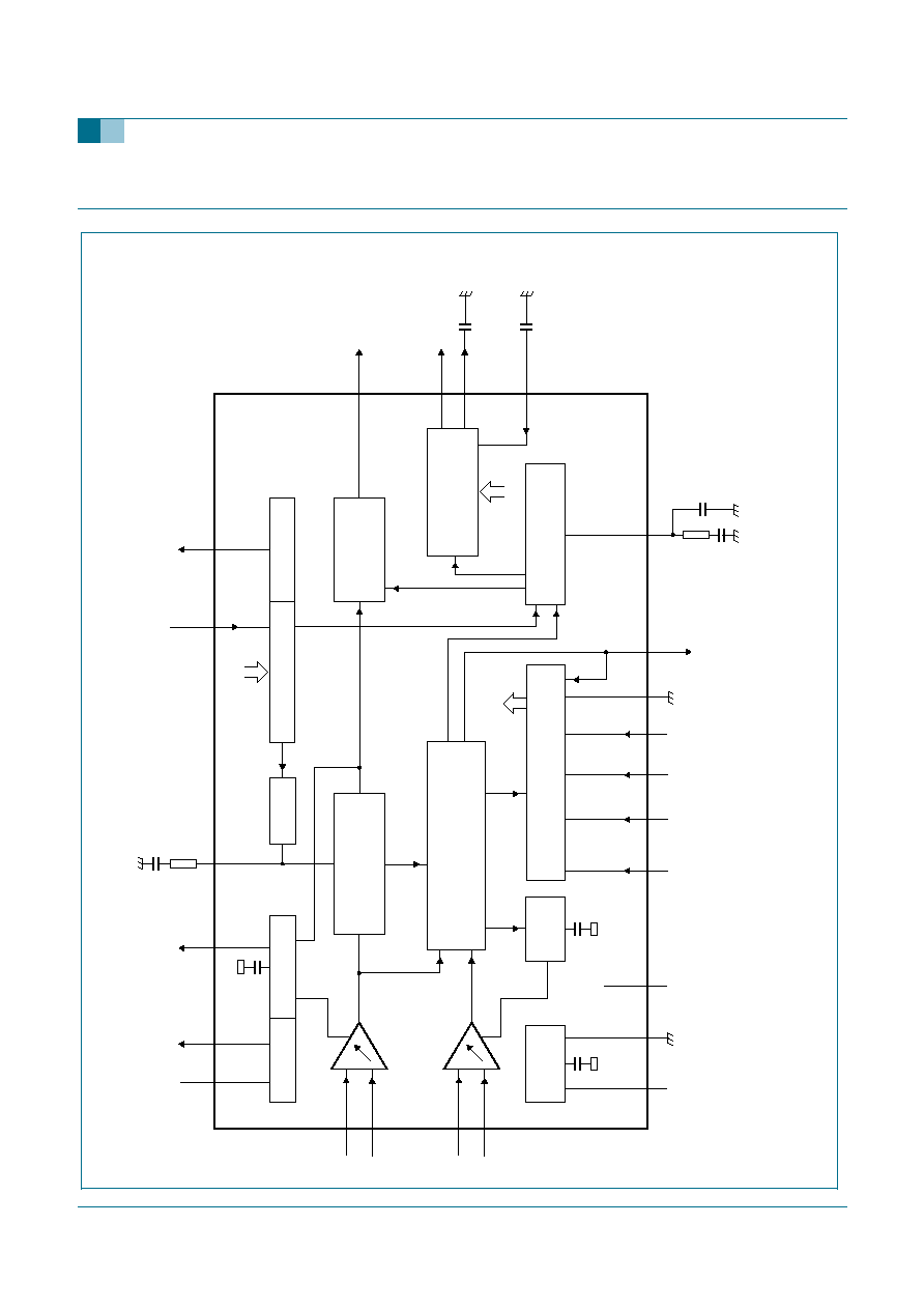
Bloc
k dia
gram
Pin numbers for TDA9881HN in parenthesis.
Fig 1.
Block diagram.
mhc504
SINGLE REFERENCE QSS MIXER
INTERCARRIER MIXER
DIGITAL VCO CONTROL
AFC DETECTOR
RC VCO
VIF PLL
VIF AGC
TUNER AGC
SUPPLY
SIF AGC
AUDIO PROCESSING
AND SWITCHES
NARROW-BAND
FM PLL DEMODULATOR
SOUND TRAPS
4.5 MHz to 6.5 MHz
TAGC
C
AGC
VAGC
TOP
14 (15)
VPLL
19 (21)
9 (8)
22 (24)
15 (16)
21 (23)
4 (2)
10 (9)
11 (10)
12 (11)
18 (20)
20 (22)
2 (31)
1 (30)
(18) 17
(7) 8
(3) 5
(4) 6
external reference signal
or 4 MHz crystal
REF
AFC
FMSO
CVBS
FM sound output
video output: 2 V (p-p)
C
AF
QSSO
FM1
FM0
VP
C
AGC
3 (1)
i.c.
AGND
7 (5)
DGND
LOGIC
13 (14)
16 (17)
AMUTE0 VIF0
FMPLL
DEEM
AFD
single reference
QSS output
FM PLL
filter
VIF PLL
filter
de-emphasis
network
VIF2
VIF1
24 (27)
23 (26)
SIF2
SIF1
TDA9881
9397 750 13417
� Koninklijke Philips Electronics N.V. 2004. All rights reserved.
Product data sheet
Rev. 01 -- 16 November 2004
5 of 42
Philips Semiconductors
TDA9881
Alignment-free vision and FM sound IF PLL demodulator
7.
Pinning information
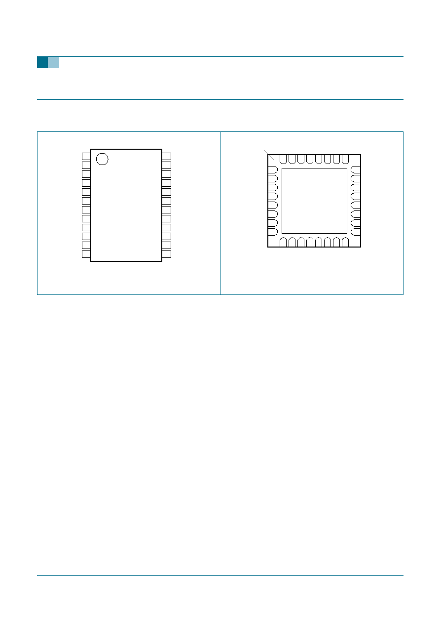
7.1 Pinning
Fig 2.
Pin configuration for SSOP24.
Fig 3.
Pin configuration for HVQFN32.
TDA9881TS
VIF1
SIF2
VIF2
SIF1
i.c.
VAGC
FMPLL
AFC
DEEM
V
P
AFD
VPLL
DGND
AGND
FMSO
CVBS
TOP
AMUTE0
FM1
REF
FM0
TAGC
QSSO
VIF0
001aab340
1
2
3
4
5
6
7
8
9
10
11
12
14
13
16
15
18
17
20
19
22
21
24
23
001aab344
TDA9881HN
Transparent top view
AMUTE0
FMSO
TOP
CVBS
n.c.
n.c.
DGND
AGND
AFD
VPLL
DEEM
V
P
FMPLL
AFC
i.c.
VAGC
FM1
FM0
QSSO
n.c.
n.c.
VIF0
TAGC
REF
n.c.
VIF2
VIF1
n.c.
n.c.
SIF2
SIF1
n.c.
8
17
7
18
6
19
5
20
4
21
3
22
2
23
1
24
9
10
11
12
13
14
15
16
32
31
30
29
28
27
26
25
terminal 1
index area

9397 750 13417
� Koninklijke Philips Electronics N.V. 2004. All rights reserved.
Product data sheet
Rev. 01 -- 16 November 2004
6 of 42
Philips Semiconductors
TDA9881
Alignment-free vision and FM sound IF PLL demodulator
7.2 Pin description
Table 3:
Pin description
Symbol
Pin
Description
TDA9881TS
TDA9881HN
VIF1
1
30
VIF differential input 1
VIF2
2
31
VIF differential input 2
n.c.
-
32
not connected
i.c.
3
1
internally connected; leave open
FMPLL
4
2
FM PLL for loop filter
DEEM
5
3
de-emphasis output for capacitor
AFD
6
4
AF decoupling input for capacitor
DGND
7
5
digital ground
n.c.
-
6
not connected
FMSO
8
7
FM sound output
TOP
9
8
tuner AGC TakeOver Point (TOP) for resistor adjustment
FM1
10
9
FM IF select bit 1
FM0
11
10
FM IF select bit 0
QSSO
12
11
single reference QSS output and vision IF select bit 1
with resistor
n.c.
-
12
not connected
n.c.
-
13
not connected
VIF0
13
14
vision IF select bit 0
TAGC
14
15
tuner AGC output
REF
15
16
4 MHz crystal or reference signal input
AMUTE0
16
17
auto mute select bit 0
CVBS
17
18
composite video output
n.c.
-
19
not connected
AGND
18
20
analog ground
VPLL
19
21
VIF PLL for loop filter
V
P
20
22
supply voltage
AFC
21
23
AFC output
VAGC
22
24
vision AGC output
n.c.
-
25
not connected
SIF1
23
26
SIF differential input 1 and intercarrier mode select
SIF2
24
27
SIF differential input 2 and intercarrier mode select
n.c.
-
28
not connected
n.c.
-
29
not connected

9397 750 13417
� Koninklijke Philips Electronics N.V. 2004. All rights reserved.
Product data sheet
Rev. 01 -- 16 November 2004
7 of 42
Philips Semiconductors
TDA9881
Alignment-free vision and FM sound IF PLL demodulator
8.
Functional description
A simplified block diagram of the device is illustrated in
Figure 1
. The device contains the
following functional blocks:
1. VIF amplifier
2. Tuner AGC and VIF AGC
3. VIF AGC detector
4. Frequency Phase-Locked Loop (FPLL) detector
5. VCO and divider
6. AFC and digital acquisition help circuit
7. Video demodulator and amplifier
8. Sound carrier trap
9. SIF amplifier
10.SIF AGC detector
11.Single reference QSS mixer
12.FM demodulator and acquisition help circuit
13.Audio amplifier and mute time constant
14.Internal voltage stabilizer
15.Logic.
8.1 VIF amplifier
The VIF amplifier consists of three AC-coupled differential stages. Gain control is
performed by emitter degeneration. The total gain control range is typical 66 dB. The
differential input impedance is typical 2 k
in parallel with 3 pF.
8.2 Tuner AGC and VIF AGC
This block adapts the voltage, generated at the VIF AGC detector, to the internal signal
processing at the VIF amplifier and performs the tuner AGC control current generation.
The onset of the tuner AGC control current generation can be set by a potentiometer at
pin TOP.
8.3 VIF AGC detector
Gain control is performed using sync level detection.
The sync level voltage is stored in an integrated capacitor by means of a fast peak
detector. This voltage is compared with a reference voltage (nominal sync level) by a
comparator which charges or discharges the integrated AGC capacitor to generate the
VIF gain. The time constants for decreasing or increasing the gain are nearly equal and
the total AGC reaction time is fast, to cope with `aeroplane fluttering'.

9397 750 13417
� Koninklijke Philips Electronics N.V. 2004. All rights reserved.
Product data sheet
Rev. 01 -- 16 November 2004
8 of 42
Philips Semiconductors
TDA9881
Alignment-free vision and FM sound IF PLL demodulator
8.4 FPLL detector
The VIF amplifier output signal is fed to a frequency detector and a phase detector via a
limiting amplifier to remove the video AM.
During acquisition the frequency detector produces a current that is proportional to the
frequency difference between the VIF and the VCO signal. After frequency lock-in the
phase detector produces a current that is proportional to the phase difference between
the VIF and the VCO signal. The currents from the frequency and phase detector are
charged into the loop filter which controls the VIF VCO and locks it to the frequency and
phase of the VIF carrier.
8.5 VCO and divider
The VCO of the VIF FPLL operates as an integrated low radiation relaxation oscillator at
twice the picture carrier frequency. The control voltage, required to tune the VCO to
actually double the picture carrier frequency, is generated at the loop filter by the
frequency phase detector. The possible frequency range is 50 MHz to 140 MHz (typical
value).
The oscillator frequency is divided-by-two to provide two differential square wave signals
with exactly 90 degrees phase difference, independent of the frequency, for use in the
FPLL detectors, the video demodulator and the single reference QSS or intercarrier mixer.
8.6 AFC and digital acquisition help circuit
Each relaxation oscillator of the VIF PLL and FM PLL demodulator has a wide frequency
range. To prevent false locking of the PLLs, with respect to the catching range, the digital
acquisition help circuit provides an individual control until the frequency of the VCO is
within the preselected standard dependent lock-in window of the PLL.
The VIF carrier frequencies 38.0 MHz, 38.9 MHz (M/N, B/G, I and D/K standard) and
45.75 MHz, 58.75 MHz (NTSC standard) can be selected via pin VIF0 and pin QSSO with
resistor; see
Table 4
.
The FM carrier frequencies can be selected via pin FM0 and pin FM1; see
Table 5
.
The in-window and out-window control at the FM PLL can additionally be used to mute the
audio stage (if auto mute is selected via pin AMUTE0); see
Table 6
.
The principle working of the digital acquisition help circuit is as follows: The PLL VCO
output is connected to a downcounter which has a predefined start value (standard
dependent). The VCO frequency clocks the downcounter for a fixed gate time. Thereafter,
the downcounter stop value is analyzed. In the event that the stop value is higher (lower)
than the expected value range, the VCO frequency will be lower (higher) than the required
lock-in window frequency range. A positive (negative) control current is injected into the
PLL loop filter which causes the VCO frequency to be increased (decreased) and a new
counting cycle starts.
The gate time as well as the control logic of the acquisition help circuit is dependent on the
precision of the reference signal at pin REF. Operation as a crystal oscillator is possible as
well as connecting this input via a serial capacitor to an external reference frequency e.g.
the tuning system oscillator.

9397 750 13417
� Koninklijke Philips Electronics N.V. 2004. All rights reserved.
Product data sheet
Rev. 01 -- 16 November 2004
9 of 42
Philips Semiconductors
TDA9881
Alignment-free vision and FM sound IF PLL demodulator
The AFC signal is derived from the corresponding downcounter stop value after a
counting cycle. The last four bits are latched and the digital-to-analog converted value is
given as current at pin AFC.
8.7 Video demodulator and amplifier
The video demodulator is realized by a multiplier which is designed for low distortion and
large bandwidth. The VIF signal is multiplied with the `in phase' signal of the VIF PLL
VCO.
The demodulator output signal is fed into the video preamplifier via a level shift stage with
integrated low-pass filter to achieve carrier harmonics attenuation.
The output signal of the preamplifier is fed to the VIF AGC detector (see
Section 8.3
) and
in the sound trap mode is also fed internally to the integrated sound carrier trap;
see
Section 8.8
. The differential trap output signal is converted and amplified by the
following postamplifier. The video output level at pin CVBS is 2 V (p-p).
Noise clipping is provided.
8.8 Sound carrier trap
The sound carrier trap consists of a reference filter, a phase detector and the sound trap
itself.
A sound carrier reference signal is fed into the reference low-pass filter and is shifted by
nominal 90 degrees. The phase detector compares the original reference signal with the
signal shifted by the reference filter and produces a DC voltage by charging or discharging
an integrated capacitor with a current proportional to the phase difference between both
signals, respectively to the frequency error of the integrated filters. The DC voltage
controls the frequency position of the reference filter and the sound trap. Thus the
accurate frequency position for the different standards is set by the sound carrier
reference signal.
The sound trap itself is constructed of three separate traps to realize sufficient
suppression of the first and second sound carrier.
8.9 SIF amplifier
The SIF amplifier consists of three AC-coupled differential stages. Gain control is
performed by emitter degeneration. The total gain control range is typical 66 dB. The
differential input impedance is typical 2 k
in parallel with 3 pF.
8.10 SIF AGC detector
SIF gain control is performed by the detection of the SIF voltage at the output of the SIF
amplifier so that a constant SIF signal is supplied to the single reference QSS mixer.
For an optimum adaption between the SIF AGC and the VIF AGC characteristics at 13 dB
picture-to-sound FM carrier ratio, the internal SIF level is reduced.
The integrated AGC capacitor is charged or discharged for the generation of the required
SIF gain via a comparator. An additional circuit (threshold approximately 7 dB) ensures a
very fast gain reduction for a large increasing IF amplitude step.

9397 750 13417
� Koninklijke Philips Electronics N.V. 2004. All rights reserved.
Product data sheet
Rev. 01 -- 16 November 2004
10 of 42
Philips Semiconductors
TDA9881
Alignment-free vision and FM sound IF PLL demodulator
8.11 Single reference QSS mixer
With the present system high performance Hi-Fi stereo sound processing can be
achieved. For a simplified application without an SIF SAW filter, the single reference QSS
mixer can be switched to the intercarrier mode via pins SIF1 and SIF2; see
Table 7
.
The single reference QSS mixer generates the 2nd FM TV sound intercarrier signal. It is
realized by a linear multiplier which multiplies the SIF amplifier output signal and the
VIF PLL VCO signal which is locked to the picture carrier. In this way the QSS mixer
operates as a quadrature mixer in the intercarrier mode and provides suppression of the
low frequency video signals.
The QSS mixer output signal is fed internally via a high-pass and low-pass combination to
the FM demodulator as well as via an operational amplifier to the QSS output pin QSSO.
8.12 FM demodulator and acquisition help circuit
The narrow-band FM PLL detector consists of:
�
Gain controlled FM amplifier and AGC detector
�
Narrow-band PLL.
The intercarrier signal from the single reference QSS mixer is fed to the input of an
AC-coupled gain controlled amplifier with two stages. The gain controlled output signal is
fed to the phase detector of the narrow-band FM PLL (FM demodulator). For good
selectivity and robustness against disturbance caused by the video signal, a high linearity
of the gain controlled FM amplifier and of the phase detector as well as a constant signal
level are required. The gain control is done by means of an `in phase' demodulator for the
FM carrier (from the output of the FM amplifier). The demodulation output is fed into a
comparator for charging or discharging the integrated AGC capacitor. This leads to a
mean value AGC loop to control the gain of the FM amplifier.
The FM demodulator is realized as a narrow-band PLL with an external loop filter, which
provides the necessary selectivity (bandwidth approximately 100 kHz). To achieve good
selectivity, a linear phase detector and a constant input level are required. The gain
controlled intercarrier signal from the FM amplifier is fed to the phase detector. The phase
detector controls, via the loop filter, the integrated low radiation relaxation oscillator. The
designed frequency range is from 4 MHz to 7 MHz.
The VCO within the FM PLL is phase-locked to the incoming 2nd SIF signal which is
frequency modulated. The VCO control voltage is superimposed by the AF voltage.
Therefore, the VCO tracks with the FM of the 2nd SIF signal. Thus, the AF voltage is
present at the loop filter and is typically 5 mV (RMS) for 27 kHz FM deviation. This
AF signal is fed via a buffer to the audio amplifier.
The correct locking of the PLL is supported by the digital acquisition help circuit; see
Section 8.6
.

9397 750 13417
� Koninklijke Philips Electronics N.V. 2004. All rights reserved.
Product data sheet
Rev. 01 -- 16 November 2004
11 of 42
Philips Semiconductors
TDA9881
Alignment-free vision and FM sound IF PLL demodulator
8.13 Audio amplifier and mute time constant
The audio amplifier consists of two parts:
�
AF preamplifier
�
AF output amplifier.
The AF preamplifier used for FM sound is an operational amplifier with internal feedback,
high gain and high common mode rejection. The AF voltage from the PLL demodulator is
5 mV (RMS) for a frequency deviation of 27 kHz and is amplified by 30 dB. By using a
DC operating point control circuit (with external capacitor C
AF
), the AF preamplifier is
decoupled from the PLL DC voltage. The low-pass characteristic of the amplifier reduces
the harmonics of the sound intercarrier signal at the AF output terminal.
For FM sound a switchable de-emphasis network (with external capacitor) is implemented
between the preamplifier and the output amplifier. The de-emphasis time constant with
50
�
s or 75
�
s depends on the FM carrier selection via pins FM0 and FM1; see
Table 5
.
The AF output amplifier provides the required AF output level by a rail-to-rail output stage.
A preceding stage makes use of an input selector for switching between the FM sound
and mute state.
Switching to the mute state is controlled automatically, depending on the digital acquisition
help circuit should the VCO of the FM PLL not be in the required frequency window. This
is done by a time constant: fast for switching to the mute state and slow (typically 40 ms)
for switching to the non-mute state.
Auto mute can be disabled via pin AMUTE0; see
Table 6
.
8.14 Internal voltage stabilizer
The band gap circuit internally generates a voltage of approximately 2.4 V, independent of
the supply voltage and the temperature. A voltage regulator circuit, connected to this
voltage, produces a constant voltage of 3.55 V which is used as an internal reference
voltage.
8.15 Logic
The logic circuit detects the logic level at the logic ports VIF0, QSSO, FM0, FM1 and
AMUTE0 and controls the internal functions; see
Table 4
to
Table 6
. In the event that all
logic ports are open-circuit (high-ohmic or CMOS HIGH level) TV standard NTSC with a
vision carrier frequency of 45.75 MHz, an FM sound carrier frequency of 4.5 MHz,
de-emphasis with 75
�
s time constant and auto mute on is selected.
Table 4:
VIF frequency selection
QSSO
VIF0
VIF frequency (MHz)
No resistor at pin
pin open-circuit
45.75
No resistor at pin
pin connected to ground
38.9
2.2 k
resistor to ground at pin pin open-circuit
58.75
2.2 k
resistor to ground at pin pin connected to ground
38.0

9397 750 13417
� Koninklijke Philips Electronics N.V. 2004. All rights reserved.
Product data sheet
Rev. 01 -- 16 November 2004
12 of 42
Philips Semiconductors
TDA9881
Alignment-free vision and FM sound IF PLL demodulator
9.
Limiting values
[1]
Class 3A according to JESD22-A114-B.
[2]
Class C according to EIA/JESD22-A115-A.
Table 5:
FM carrier frequency selection and de-emphasis settings
FM0
FM1
FM carrier frequency
(MHz)
De-emphasis (
�
s)
Pin open-circuit
pin open-circuit
4.5
75
Pin connected to
ground
pin open-circuit
5.5
50
Pin open-circuit
pin connected to
ground
6.0
50
Pin connected to
ground
pin connected to
ground
6.5
50
Table 6:
Auto mute on/off selection
AMUTE0
Auto mute
Pin open-circuit
on
Pin connected to ground
off
Table 7:
Sound carrier mode
SIF1 and SIF2
Sound mode
No DC path to ground
QSS mode
One or both pins connected to ground
intercarrier mode
Table 8:
Limiting values
In accordance with the Absolute Maximum Rating System (IEC 60134).
Symbol
Parameter
Conditions
Min
Max
Unit
V
P
supply voltage
-
5.5
V
V
n
voltage on
all pins except AGND,
DGND and TAGC
0
V
P
V
pin TAGC
0
8.8
V
t
sc
short-circuit time to ground
or V
P
-
10
s
T
stg
storage temperature
-
25
+150
�
C
T
amb
ambient temperature
TDA9881TS (SSOP24)
-
20
+70
�
C
TDA9881HN (HVQFN32)
-
20
+85
�
C
V
esd
electrostatic discharge
voltage
human body
model
[1]
-
�
4000
V
machine model
[2]
-
�
400
V

9397 750 13417
� Koninklijke Philips Electronics N.V. 2004. All rights reserved.
Product data sheet
Rev. 01 -- 16 November 2004
13 of 42
Philips Semiconductors
TDA9881
Alignment-free vision and FM sound IF PLL demodulator
10. Thermal characteristics
11. Characteristics
Table 9:
Thermal characteristics
Symbol
Parameter
Conditions
Typ
Unit
R
th(j-a)
thermal resistance from junction to ambient
in free air
TDA9881TS (SSOP24)
105
K/W
TDA9881HN (HVQFN32)
40
K/W
Table 10:
Characteristics
V
P
= 5 V; T
amb
= 25
�
C; see
Table 12
for input frequencies; B/G standard is used for the specification (f
PC
= 38.9 MHz;
f
SC
= 33.4 MHz; PC/SC = 13 dB; f
mod
= 400 Hz); input level V
i(VIF)
= 10 mV (RMS) (sync level for B/G); IF input from 50
via
broadband transformer 1 : 1; video modulation DSB; residual carrier for B/G is 10 %; video signal in accordance with "CCIR
line 17 and line 330"; measurements taken in test circuit of
Figure 21
; unless otherwise specified.
Symbol
Parameter
Conditions
Min
Typ
Max
Unit
Supply; pin V
P
V
P
supply voltage
[1]
4.5
5.0
5.5
V
I
P
supply current
52
63
70
mA
P
tot
total power dissipation
-
305
385
mW
Power-on reset
V
P(start)
supply voltage for start of
reset
decreasing supply
voltage
2.5
3.0
3.5
V
V
P(stop)
supply voltage for end of
reset
increasing supply
voltage
-
-
4.4
V
P
time constant (R
�
C) for
network at pin V
P
1.2
-
-
�
s
VIF amplifier; pins VIF1 and VIF2
V
i(VIF)(rms)
VIF input voltage
sensitivity (RMS value)
-
1 dB video at output
-
60
100
�
V
V
i(max)(rms)
maximum input voltage
(RMS value)
+1 dB video at output
150
190
-
mV
V
i(ovl)(rms)
overload input voltage
(RMS value)
[2]
-
-
440
mV
V
IF(int)
internal IF amplitude
difference between
picture and sound carrier
within AGC range;
f = 5.5 MHz
-
0.9
-
dB
G
VIF(cr)
VIF gain control range
see
Figure 6
60
66
-
dB
B
VIF(
-
3dB)(ll)
lower limit
-
3 dB VIF
bandwidth
-
15
-
MHz
B
VIF(
-
3dB)(ul)
upper limit
-
3 dB VIF
bandwidth
-
80
-
MHz
R
i(dif)
differential input
resistance
[3]
-
2
-
k
C
i(dif)
differential input
capacitance
[3]
-
3
-
pF
V
I
DC input voltage
-
1.93
-
V

9397 750 13417
� Koninklijke Philips Electronics N.V. 2004. All rights reserved.
Product data sheet
Rev. 01 -- 16 November 2004
14 of 42
Philips Semiconductors
TDA9881
Alignment-free vision and FM sound IF PLL demodulator
FPLL and true synchronous video demodulator
[4]
f
VCO(max)
maximum oscillator
frequency for carrier
regeneration
f = 2f
PC
120
140
-
MHz
f
VIF
vision carrier operating
frequencies
see
Table 4
-
38.0
-
MHz
-
38.9
-
MHz
-
45.75
-
MHz
-
58.75
-
MHz
f
VIF
VIF frequency window of
digital acquisition help
related to f
VIF
;
see
Figure 9
-
�
2.3
-
MHz
t
acq
acquisition time
BL = 70 kHz
[5]
-
-
30
ms
V
i(lock)(rms)
input voltage sensitivity
for PLL to be locked
(RMS value)
measured on pins VIF1
and VIF2; maximum
IF gain
-
50
100
�
V
T
cy(DAH)
cycle time of digital
acquisition help
-
64
-
�
s
K
O(VIF)
VIF VCO steepness
definition:
f
VIF
/
V
VPLL
-
20
-
MHz/V
K
D(VIF)
VIF phase detector
steepness
definition:
I
VPLL
/
VIF
-
23
-
�
A/rad
Video output 2 V; pin CVBS; sound carrier on
V
o(p-p)
video output voltage
(peak-to-peak value)
see
Figure 4
1.7
2.0
2.3
V
V/S
ratio between video
(black-to-white) and sync
level
1.90
2.33
3.00
V
sync
sync voltage level
1.0
1.2
1.4
V
V
clip(u)
upper video clipping
voltage level
V
P
-
1.1
V
P
-
1
-
V
V
clip(l)
lower video clipping
voltage level
-
0.7
0.9
V
R
o
output resistance
[3]
-
-
30
I
bias(int)
internal DC bias current
for emitter-follower
1.5
2.0
-
mA
I
o(sink)(max)
maximum AC and DC
output sink current
1
-
-
mA
I
o(source)(max)
maximum AC and DC
output source current
3.9
-
-
mA
V
o(CVBS)
deviation of CVBS output
voltage
50 dB gain control
-
-
0.5
dB
30 dB gain control
-
-
0.1
dB
V
o(bl)
black level tilt
-
-
2
%
G
dif
differential gain
"CCIR 330";
B/G standard
[6]
-
-
5
%
Table 10:
Characteristics
...continued
V
P
= 5 V; T
amb
= 25
�
C; see
Table 12
for input frequencies; B/G standard is used for the specification (f
PC
= 38.9 MHz;
f
SC
= 33.4 MHz; PC/SC = 13 dB; f
mod
= 400 Hz); input level V
i(VIF)
= 10 mV (RMS) (sync level for B/G); IF input from 50
via
broadband transformer 1 : 1; video modulation DSB; residual carrier for B/G is 10 %; video signal in accordance with "CCIR
line 17 and line 330"; measurements taken in test circuit of
Figure 21
; unless otherwise specified.
Symbol
Parameter
Conditions
Min
Typ
Max
Unit

9397 750 13417
� Koninklijke Philips Electronics N.V. 2004. All rights reserved.
Product data sheet
Rev. 01 -- 16 November 2004
15 of 42
Philips Semiconductors
TDA9881
Alignment-free vision and FM sound IF PLL demodulator
dif
differential phase
"CCIR 330"
-
2
4
deg
S/N
W(video)
weighted signal-to-noise
ratio
weighted in accordance
with
"CCIR 567";
see
Figure 10
[7]
55
-
-
dB
S/N
UW(video)
unweighted
signal-to-noise ratio
[7]
47
-
-
dB
IM(blue)
intermodulation
attenuation at `blue'
see
Figure 11
[8]
f = 1.1 MHz
58
64
-
dB
f = 3.3 MHz
58
64
-
dB
IM(yellow)
intermodulation
attenuation at `yellow'
see
Figure 11
[8]
f = 1.1 MHz
60
66
-
dB
f = 3.3 MHz
59
65
-
dB
V
r(PC)(rms)
residual picture carrier
(RMS value)
fundamental wave and
harmonics
-
2
5
mV
H
suppression of video
signal harmonics
C
L
< 20 pF; R
L
> 1 k
;
AC load
[9]
35
40
-
dB
spur
suppression of spurious
elements
[10]
40
-
-
dB
PSRR
CVBS
power supply ripple
rejection at pin CVBS
f
ripple
= 70 Hz;
see
Figure 5
[11]
20
25
-
dB
M/N standard inclusive Korea; see
Figure 12
B
v(
-
3dB)(trap)
-
3 dB video bandwidth
including sound carrier
trap
f
trap
= 4.5 MHz
[12]
3.95
4.05
-
MHz
SC1
attenuation at first sound
carrier
f = 4.5 MHz
26
36
-
dB
SC1(60kHz)
attenuation at first sound
carrier f
SC1
�
60 kHz
f = 4.5 MHz
20
27
-
dB
SC2
attenuation at second
sound carrier
f = 4.724 MHz
20
27
-
dB
SC2(60kHz)
attenuation at second
sound carrier
f
SC2
�
60 kHz
f = 4.724 MHz
14
21
-
dB
t
d(g)(cc)
group delay at color
carrier frequency
f = 3.58 MHz;
see
Figure 13
110
180
250
ns
B/G standard; see
Figure 14
B
v(
-
3dB)(trap)
-
3 dB video bandwidth
including sound carrier
trap
f
trap
= 5.5 MHz
[12]
4.90
5.00
-
MHz
SC1
attenuation at first sound
carrier
f = 5.5 MHz
26
36
-
dB
SC1(60kHz)
attenuation at first sound
carrier f
SC1
�
60 kHz
f = 5.5 MHz
20
30
-
dB
Table 10:
Characteristics
...continued
V
P
= 5 V; T
amb
= 25
�
C; see
Table 12
for input frequencies; B/G standard is used for the specification (f
PC
= 38.9 MHz;
f
SC
= 33.4 MHz; PC/SC = 13 dB; f
mod
= 400 Hz); input level V
i(VIF)
= 10 mV (RMS) (sync level for B/G); IF input from 50
via
broadband transformer 1 : 1; video modulation DSB; residual carrier for B/G is 10 %; video signal in accordance with "CCIR
line 17 and line 330"; measurements taken in test circuit of
Figure 21
; unless otherwise specified.
Symbol
Parameter
Conditions
Min
Typ
Max
Unit

9397 750 13417
� Koninklijke Philips Electronics N.V. 2004. All rights reserved.
Product data sheet
Rev. 01 -- 16 November 2004
16 of 42
Philips Semiconductors
TDA9881
Alignment-free vision and FM sound IF PLL demodulator
SC2
attenuation at second
sound carrier
f = 5.742 MHz
20
27
-
dB
SC2(60kHz)
attenuation at second
sound carrier
f
SC2
�
60 kHz
f = 5.742 MHz
14
21
-
dB
t
d(g)(cc)
group delay at color
carrier frequency
f = 4.43 MHz;
see
Figure 15
110
180
250
ns
I standard; see
Figure 16
B
v(
-
3dB)(trap)
-
3 dB video bandwidth
including sound carrier
trap
f
trap
= 6.0 MHz
[12]
5.40
5.50
-
MHz
SC1
attenuation at first sound
carrier
f = 6.0 MHz
26
32
-
dB
SC1(60kHz)
attenuation at first sound
carrier f
SC1
�
60 kHz
f = 6.0 MHz
20
26
-
dB
SC2
attenuation at second
sound carrier
f = 6.55 MHz
12
18
-
dB
SC2(60kHz)
attenuation at second
sound carrier
f
SC2
�
60 kHz
f = 6.55 MHz
10
15
-
dB
t
d(g)(cc)
group delay at color
carrier frequency
f = 4.43 MHz
-
90
160
ns
D/K standard; see
Figure 17
B
v(
-
3dB)(trap)
-
3 dB video bandwidth
including sound carrier
trap
f
trap
= 6.5 MHz
[12]
5.50
5.95
-
MHz
SC1
attenuation at first sound
carrier
f = 6.5 MHz
26
32
-
dB
SC1(60kHz)
attenuation at first sound
carrier f
SC1
�
60 kHz
f = 6.5 MHz
20
26
-
dB
SC2
attenuation at second
sound carrier
f = 6.742 MHz
18
24
-
dB
SC2(60kHz)
attenuation at second
sound carrier
f
SC2
�
60 kHz
f = 6.742 MHz
13
18
-
dB
t
d(g)(cc)
group delay at color
carrier frequency
f = 4.28 MHz
-
60
130
ns
VIF AGC
t
resp(inc)
AGC response time to an
increasing VIF step
20 dB
[13]
-
4
-
ms
t
resp(dec)
AGC response time to a
decreasing VIF step
20 dB
[13]
-
3
-
ms
Table 10:
Characteristics
...continued
V
P
= 5 V; T
amb
= 25
�
C; see
Table 12
for input frequencies; B/G standard is used for the specification (f
PC
= 38.9 MHz;
f
SC
= 33.4 MHz; PC/SC = 13 dB; f
mod
= 400 Hz); input level V
i(VIF)
= 10 mV (RMS) (sync level for B/G); IF input from 50
via
broadband transformer 1 : 1; video modulation DSB; residual carrier for B/G is 10 %; video signal in accordance with "CCIR
line 17 and line 330"; measurements taken in test circuit of
Figure 21
; unless otherwise specified.
Symbol
Parameter
Conditions
Min
Typ
Max
Unit

9397 750 13417
� Koninklijke Philips Electronics N.V. 2004. All rights reserved.
Product data sheet
Rev. 01 -- 16 November 2004
17 of 42
Philips Semiconductors
TDA9881
Alignment-free vision and FM sound IF PLL demodulator
CR
stps
control steepness
definition:
G
VIF
/
V
VAGC
;
V
VAGC
= 2 V to 3 V
-
-
80
-
dB/V
Pin VAGC
V
VAGC
gain control voltage
range
see
Figure 6
0.8
-
3.5
V
I
o(sink)(max)
maximum output sink
current
-
-
10
�
A
I
o(source)(max)
maximum output source
current
-
-
10
�
A
Tuner AGC; pin TAGC; see
Figure 6
to
Figure 8
V
i(VIF)(start1)(rms)
VIF input signal voltage
for minimum starting
point of tuner takeover at
pins VIF1 and VIF2
(RMS value)
I
TAGC
= 120
�
A;
R
TOP
= 22 k
-
2
5
mV
V
i(VIF)(start2)(rms)
VIF input signal voltage
for maximum starting
point of tuner takeover at
pins VIF1 and VIF2
(RMS value)
I
TAGC
= 120
�
A;
R
TOP
= 0
45
90
-
mV
QV
TOP
tuner takeover point
accuracy
I
TAGC
= 120
�
A;
R
TOP
= 10 k
7
17
43
mV
QV
TOP
/
T
takeover point variation
with temperature
I
TAGC
= 120
�
A
-
0.03
0.07
dB/K
V
o
permissible output
voltage
from external source
-
-
8.8
V
V
sat
saturation voltage
I
TAGC
= 450
�
A
-
-
0.5
V
I
sink
sink current
no tuner gain reduction;
V
TAGC
= 8.8 V
-
-
0.75
�
A
maximum tuner gain
reduction; V
TAGC
= 1 V
450
600
750
�
A
G
IF
IF slip by automatic gain
control
tuner gain current from
20 % to 80 %
3
5
8
dB
AFC circuit; pin AFC; see
Figure 9
[14] [15]
AFC
stps
AFC control steepness
definition:
I
AFC
/
f
VIF
0.85
1.05
1.25
�
A/kHz
Qf
VIF(a)
analog accuracy of AFC
circuit
I
AFC
= 0 A;
f
REF
= 4 MHz
-
20
-
+20
kHz
V
sat(ul)
upper limit saturation
voltage
V
P
-
0.6
V
P
-
0.3
-
V
V
sat(ll)
lower limit saturation
voltage
-
0.3
0.6
V
I
o(source)
output source current
160
200
240
�
A
I
o(sink)
output sink current
160
200
240
�
A
Table 10:
Characteristics
...continued
V
P
= 5 V; T
amb
= 25
�
C; see
Table 12
for input frequencies; B/G standard is used for the specification (f
PC
= 38.9 MHz;
f
SC
= 33.4 MHz; PC/SC = 13 dB; f
mod
= 400 Hz); input level V
i(VIF)
= 10 mV (RMS) (sync level for B/G); IF input from 50
via
broadband transformer 1 : 1; video modulation DSB; residual carrier for B/G is 10 %; video signal in accordance with "CCIR
line 17 and line 330"; measurements taken in test circuit of
Figure 21
; unless otherwise specified.
Symbol
Parameter
Conditions
Min
Typ
Max
Unit

9397 750 13417
� Koninklijke Philips Electronics N.V. 2004. All rights reserved.
Product data sheet
Rev. 01 -- 16 November 2004
18 of 42
Philips Semiconductors
TDA9881
Alignment-free vision and FM sound IF PLL demodulator
SIF amplifier; pins SIF1 and SIF2
V
i(SIF)(rms)
SIF input voltage
sensitivity (RMS value)
-
3 dB at intercarrier
output pin QSSO
-
30
70
�
V
V
i(max)(rms)
maximum input voltage
(RMS value)
1 dB at intercarrier
output pin QSSO
50
70
-
mV
V
i(ovl)(rms)
overload input voltage
(RMS value)
[2]
-
-
320
mV
G
SIF(cr)
SIF gain control range
see
Figure 8
60
66
-
dB
B
SIF(
-
3dB)(ll)
lower limit
-
3 dB SIF
bandwidth
-
15
-
MHz
B
SIF(
-
3dB)(ul)
upper limit
-
3 dB SIF
bandwidth
-
80
-
MHz
R
i(dif)
differential input
resistance
[3]
-
2
-
k
C
i(dif)
differential input
capacitance
[3]
-
3
-
pF
V
I
DC input voltage
-
1.93
-
V
SIF AGC detector
t
resp
AGC response time to an
increasing or decreasing
SIF step of 20 dB
increasing
-
8
-
ms
decreasing
-
25
-
ms
Single reference QSS intercarrier mixer; pin QSSO
V
o(intc)(rms)
IF intercarrier output level
(RMS value)
QSS mode;
SC
1
; SC
2
off
90
140
210
mV
intercarrier mode;
PC/SC
1
= 20 dB;
SC
2
off
[16]
-
75
-
mV
B
intc(
-
3dB)(ul)
upper limit
-
3 dB
intercarrier bandwidth
12
15
-
MHz
V
r(SC)(rms)
residual sound carrier
(RMS value)
fundamental wave and
harmonics
-
2
5
mV
V
r(PC)(rms)
residual picture carrier
(RMS value)
fundamental wave and
harmonics
-
2
5
mV
R
o
output resistance
[3]
-
-
30
V
O
DC output voltage
-
2
-
V
I
bias(int)
internal DC bias current
for emitter follower
0.9
1.3
-
mA
I
o(sink)(max)
maximum AC output sink
current
0.6
0.8
-
mA
I
o(source)(max)
maximum AC output
source current
0.6
0.8
-
mA
I
o(source)
DC output source current QSSO = 0; see
Table 4
[17]
0.75
0.93
1.20
mA
Table 10:
Characteristics
...continued
V
P
= 5 V; T
amb
= 25
�
C; see
Table 12
for input frequencies; B/G standard is used for the specification (f
PC
= 38.9 MHz;
f
SC
= 33.4 MHz; PC/SC = 13 dB; f
mod
= 400 Hz); input level V
i(VIF)
= 10 mV (RMS) (sync level for B/G); IF input from 50
via
broadband transformer 1 : 1; video modulation DSB; residual carrier for B/G is 10 %; video signal in accordance with "CCIR
line 17 and line 330"; measurements taken in test circuit of
Figure 21
; unless otherwise specified.
Symbol
Parameter
Conditions
Min
Typ
Max
Unit

9397 750 13417
� Koninklijke Philips Electronics N.V. 2004. All rights reserved.
Product data sheet
Rev. 01 -- 16 November 2004
19 of 42
Philips Semiconductors
TDA9881
Alignment-free vision and FM sound IF PLL demodulator
FM PLL demodulator
[15]
and
[18]
to
[22]
Sound intercarrier output; pin QSSO
V
FM(rms)
IF intercarrier level for
gain controlled operation
of FM PLL (RMS value)
corresponding PC/SC
ratio at input pins VIF1
and VIF2 is 7 dB to
47 dB
3.2
-
320
mV
V
FM(lock)(rms)
IF intercarrier level for
lock-in of PLL
(RMS value)
-
-
2
mV
V
FM(det)(rms)
IF intercarrier level for FM
carrier detect
(RMS value)
-
-
2.3
mV
f
FM
sound intercarrier
operating
FM frequencies
see
Table 5
-
4.5
-
MHz
-
5.5
-
MHz
-
6.0
-
MHz
-
6.5
-
MHz
FM sound output; pin FMSO
V
o(AF)(rms)
AF output voltage
(RMS value)
25 kHz FM deviation;
75
�
s de-emphasis
400
500
600
mV
27 kHz FM deviation;
50
�
s de-emphasis
430
540
650
mV
V
o(AF)(cl)(rms)
AF output clipping level
(RMS value)
THD < 1.5 %
1.3
1.4
-
V
V
o(AF)
/
T
AF output voltage
variation with
temperature
-
3
�
10
-
3
7
�
10
-
3
dB/K
THD
total harmonic distortion
-
0.15
0.50
%
f
AF
frequency deviation
THD < 1.5 %
[19]
-
-
�
55
kHz
B
AF(
-
3dB)
-
3 dB AF bandwidth
without de-emphasis;
measured with FM PLL
filter of
Figure 21
80
100
-
kHz
S/N
W(AF)
weighted signal-to-noise
ratio of audio signal
FM PLL only;
27 kHz FM deviation;
50
�
s de-emphasis
52
56
-
dB
black picture;
see
Figure 18
50
56
-
dB
V
r(SC)(rms)
residual sound carrier
(RMS value)
fundamental wave and
harmonics; without
de-emphasis
-
-
2
mV
AM(sup)
AM suppression of
FM demodulator
referenced to 27 kHz
FM deviation; 50
�
s
de-emphasis;
AM: f = 1 kHz;
m = 54 %
40
46
-
dB
Table 10:
Characteristics
...continued
V
P
= 5 V; T
amb
= 25
�
C; see
Table 12
for input frequencies; B/G standard is used for the specification (f
PC
= 38.9 MHz;
f
SC
= 33.4 MHz; PC/SC = 13 dB; f
mod
= 400 Hz); input level V
i(VIF)
= 10 mV (RMS) (sync level for B/G); IF input from 50
via
broadband transformer 1 : 1; video modulation DSB; residual carrier for B/G is 10 %; video signal in accordance with "CCIR
line 17 and line 330"; measurements taken in test circuit of
Figure 21
; unless otherwise specified.
Symbol
Parameter
Conditions
Min
Typ
Max
Unit

9397 750 13417
� Koninklijke Philips Electronics N.V. 2004. All rights reserved.
Product data sheet
Rev. 01 -- 16 November 2004
20 of 42
Philips Semiconductors
TDA9881
Alignment-free vision and FM sound IF PLL demodulator
PSRR
FM
power supply ripple
rejection
f
ripple
= 70 Hz;
see
Figure 5
14
20
-
dB
FM PLL filter; pin FMPLL
V
loop
DC loop voltage
1.5
-
3.3
V
I
o(source)(PD)(max)
maximum phase detector
output source current
-
60
-
�
A
I
o(sink)(PD)(max)
maximum phase detector
output sink current
-
60
-
�
A
I
o(source)(DAH)
output source current of
digital acquisition help
-
55
-
�
A
I
o(sink)(DAH)
output sink current of
digital acquisition help
-
55
-
�
A
t
W(DAH)
pulse width of digital
acquisition help current
-
16
-
�
s
T
cy(DAH)
cycle time of digital
acquisition help
-
64
-
�
s
K
O(FM)
VCO steepness
definition:
f
FM
/
V
FMPLL
-
3.3
-
MHz/V
K
D(FM)
phase detector
steepness
definition:
I
FMPLL
/
FM
-
4
-
�
A/rad
Audio amplifier
De-emphasis network; pin DEEM
R
o
output resistance
50
�
s de-emphasis;
see
Table 5
4.4
5.0
5.6
k
75
�
s de-emphasis;
see
Table 5
6.6
7.5
8.4
k
V
AF(rms)
audio signal (RMS value) f
AF
= 400 Hz;
V
FMSO
= 500 mV
-
170
-
mV
V
O
DC output voltage
-
2.37
-
V
AF decoupling; pin AFD
V
dec
DC decoupling voltage
dependent on f
FM
intercarrier frequency
1.5
-
3.3
V
I
L
leakage current
V
O(FMSO)
<
�
50 mV
-
-
�
25
nA
I
ch(max)
maximum charge current
1.15
1.50
1.85
�
A
I
dch(max)
maximum discharge
current
1.15
1.50
1.85
�
A
FM sound output; pin FMSO
R
o
output resistance
[3]
-
-
300
V
O(FMSO)
DC output voltage
-
2.37
-
V
R
L
load resistance
AC-coupled
10
-
-
k
R
L(DC)
DC load resistance
100
-
-
k
C
L
load capacitance
-
-
1.5
nF
Table 10:
Characteristics
...continued
V
P
= 5 V; T
amb
= 25
�
C; see
Table 12
for input frequencies; B/G standard is used for the specification (f
PC
= 38.9 MHz;
f
SC
= 33.4 MHz; PC/SC = 13 dB; f
mod
= 400 Hz); input level V
i(VIF)
= 10 mV (RMS) (sync level for B/G); IF input from 50
via
broadband transformer 1 : 1; video modulation DSB; residual carrier for B/G is 10 %; video signal in accordance with "CCIR
line 17 and line 330"; measurements taken in test circuit of
Figure 21
; unless otherwise specified.
Symbol
Parameter
Conditions
Min
Typ
Max
Unit

9397 750 13417
� Koninklijke Philips Electronics N.V. 2004. All rights reserved.
Product data sheet
Rev. 01 -- 16 November 2004
21 of 42
Philips Semiconductors
TDA9881
Alignment-free vision and FM sound IF PLL demodulator
B
AF(
-
3dB)(ul)
upper limit
-
3 dB
AF bandwidth of audio
amplifier
150
-
-
kHz
B
AF(
-
3dB)(ll)
lower limit
-
3 dB
AF bandwidth of audio
amplifier
[20]
-
-
20
Hz
mute
mute attenuation of
AF signal
via pin AMUTE0;
see
Table 6
70
75
-
dB
V
jump
DC jump voltage for
switching AF output to
mute state or vice versa
activated by digital
acquisition help; auto
mute on; see
Table 6
-
�
50
�
150
mV
FM operation
[21] [23]
Intercarrier AF performance
[24]
S/N
W
weighted signal-to-noise
ratio
PC/SC ratio is 21 dB to
27 dB at pins VIF1 and
VIF2
black picture
49
-
-
dB
white picture
45
-
-
dB
6 kHz sine wave
(black-to-white
modulation)
40
-
-
dB
sound carrier
subharmonics;
f = 2.75 MHz
�
3 kHz
35
-
-
dB
Single reference QSS AF performance
[25] [26]
S/N
W(SC1)
weighted signal-to-noise
ratio for SC
1
VIF input sound carrier
suppression: PC/SC
1
ratio at pins VIF1 and
VIF2 > 40 dB
black picture
51
-
-
dB
white picture
48
-
-
dB
6 kHz sine wave
(black-to-white
modulation)
42
-
-
dB
250 kHz square wave
(black-to-white
modulation)
40
-
-
dB
sound carrier
subharmonics;
f = 2.75 MHz
�
3 kHz
43
-
-
dB
sound carrier
subharmonics;
f = 2.87 MHz
�
3 kHz
44
-
-
dB
Table 10:
Characteristics
...continued
V
P
= 5 V; T
amb
= 25
�
C; see
Table 12
for input frequencies; B/G standard is used for the specification (f
PC
= 38.9 MHz;
f
SC
= 33.4 MHz; PC/SC = 13 dB; f
mod
= 400 Hz); input level V
i(VIF)
= 10 mV (RMS) (sync level for B/G); IF input from 50
via
broadband transformer 1 : 1; video modulation DSB; residual carrier for B/G is 10 %; video signal in accordance with "CCIR
line 17 and line 330"; measurements taken in test circuit of
Figure 21
; unless otherwise specified.
Symbol
Parameter
Conditions
Min
Typ
Max
Unit

9397 750 13417
� Koninklijke Philips Electronics N.V. 2004. All rights reserved.
Product data sheet
Rev. 01 -- 16 November 2004
22 of 42
Philips Semiconductors
TDA9881
Alignment-free vision and FM sound IF PLL demodulator
[1]
Values of video and sound parameters can be decreased at V
P
= 4.5 V.
S/N
W(SC2)
weighted signal-to-noise
ratio for SC
2
VIF input sound carrier
suppression: PC/SC
2
ratio at pins VIF1 and
VIF2 > 40 dB
black picture
46
-
-
dB
white picture
45
-
-
dB
6 kHz sine wave
(black-to-white
modulation)
41
-
-
dB
250 kHz square wave
(black-to-white
modulation)
29
-
-
dB
sound carrier
subharmonics;
f = 2.75 MHz
�
3 kHz
42
-
-
dB
sound carrier
subharmonics;
f = 2.87 MHz
�
3 kHz
43
-
-
dB
Reference frequency input; pin REF
V
I
DC input voltage
2.3
2.6
2.9
V
R
i
input resistance
[3]
-
5
-
k
R
xtal
resonance resistance of
crystal
operation as crystal
oscillator
-
-
200
C
x
pull-up or pull-down
capacitance
[27]
-
-
-
pF
f
ref
reference signal
frequency
[28]
-
4
-
MHz
f
ref
tolerance of reference
signal frequency
[15]
-
-
�
0.1
%
V
ref(rms)
reference signal voltage
(RMS value)
operation as input
terminal
80
-
400
mV
R
o(ref)
output resistance of
reference signal source
-
-
4.7
k
C
K
decoupling capacitance
to external reference
signal source
operation as input
terminal
22
100
-
pF
Logic; pins FM1, FM0, VIF0 and AMUTE0; see
Table 4
to
Table 6
V
i
input voltage
for LOW level
0
-
0.8
V
for HIGH level
2.5
-
V
P
V
V
i(open)
free-running voltage
pin open-circuit;
I
i
< 0.1
�
A
-
V
P
-
V
R
i
internal pull-up
resistance
37.5
-
62.5
k
Table 10:
Characteristics
...continued
V
P
= 5 V; T
amb
= 25
�
C; see
Table 12
for input frequencies; B/G standard is used for the specification (f
PC
= 38.9 MHz;
f
SC
= 33.4 MHz; PC/SC = 13 dB; f
mod
= 400 Hz); input level V
i(VIF)
= 10 mV (RMS) (sync level for B/G); IF input from 50
via
broadband transformer 1 : 1; video modulation DSB; residual carrier for B/G is 10 %; video signal in accordance with "CCIR
line 17 and line 330"; measurements taken in test circuit of
Figure 21
; unless otherwise specified.
Symbol
Parameter
Conditions
Min
Typ
Max
Unit

9397 750 13417
� Koninklijke Philips Electronics N.V. 2004. All rights reserved.
Product data sheet
Rev. 01 -- 16 November 2004
23 of 42
Philips Semiconductors
TDA9881
Alignment-free vision and FM sound IF PLL demodulator
[2]
Level headroom for input level jumps during gain control setting.
[3]
This parameter is not tested during the production and is only given as application information for designing the receiver circuit.
[4]
Loop bandwidth BL = 70 kHz (damping factor d = 1.9; calculated with sync level within gain control range). Calculation of the VIF PLL
filter can be done by use of the following formula:
, valid for d
1.2
,
where:
K
O
is the VCO steepness
or
; K
D
is the phase detector steepness
;
R is the loop resistor; C is the loop capacitor; BL
-
3dB
is the loop bandwidth for
-
3 dB; d is the damping factor.
[5]
V
i(VIF)
= 10 mV (RMS);
f = 1 MHz (VCO frequency offset related to picture carrier frequency); white picture video modulation.
[6]
Condition: luminance range (5 steps) from 0 % to 100 %.
[7]
S/N
W(video)
is the ratio of black-to-white amplitude to the black level noise voltage (RMS value measured on pin CVBS). B = 5 MHz (B/G,
I and D/K standard). Noise analyzer setting: 200 kHz high-pass and SC-trap switched on.
[8]
The intermodulation figures are defined for:
a) f = 1.1 MHz (referenced to black and white signal) as
b) f = 3.3 MHz (referenced to color carrier) as
[9]
Modulation Vestigial Side-Band (VSB); sound carrier off; f
video
> 0.5 MHz. Measurements taken with SAW filter M1963M (sound shelf:
20 dB); loop bandwidth BL = 70 kHz.
[10] Sound carrier on; f
video
= 10 kHz to 10 MHz. Measurements taken with SAW filter M1963M (sound shelf: 20 dB); loop bandwidth
BL = 70 kHz.
[11] Conditions: video signal, grey level and negative modulation.
[12] AC load; C
L
< 20 pF and R
L
> 1 k
. The sound carrier frequencies (depending on TV standard) are attenuated by the integrated sound
carrier traps (see
Figure 12
to
Figure 17
;
H(s)
is the absolute value of transfer function).
[13] The response time is valid for a VIF input level range from 200
�
V to 70 mV.
[14] To match the AFC output signal to different tuning systems a current source output is provided. The test circuit is given in
Figure 9
. The
AFC slope (voltage per frequency) can be changed by resistors R1 and R2.
[15] The tolerance of the reference frequency determines the accuracy of the VIF AFC, FM demodulator center frequency and maximum
FM deviation.
[16] The intercarrier output signal at pin QSSO can be calculated by the following formula taking into account the internal video signal with
1.1 V (p-p) as a reference:
(RMS)
where:
is the correction term for RMS value,
is the sound-to-picture carrier ratio at pins VIF1 and VIF2 in dB, 6 dB is
the correction term of internal circuitry and
�
3 dB is the tolerance of video output and intercarrier output V
o(intc)(rms)
.
[17] To detect a logical 1 at pin QSSO, no DC load at pin QSSO is allowed. QSSO = 0 will be done by the application of a 2.2 k
resistor
between pin QSSO and ground.
[18] SIF input level is 10 mV (RMS); VIF input level is 10 mV (RMS) unmodulated.
[19] Measured with an FM deviation of 25 kHz and the typical AF output voltage of 500 mV (RMS). For handling a frequency deviation of
more than 55 kHz, the AF output signal has to be reduced in order to avoid clipping (THD < 1.5 %) by means of a resistor R
x
with
external application at pin AFD (see
Figure 20
and
Figure 21
).
[20] The lower limit of the audio bandwidth depends on the value of the capacitor at pin AFD. A value of C
AF
= 470 nF leads to
f
AF(
-
3dB)
20 Hz and C
AF
= 220 nF leads to f
AF(
-
3dB)
40 Hz.
BL
3dB
�
1
2
------
K
O
K
D
R
=
d
1
2
---
R K
O
K
D
C
=
rad
V
-------
2
Hz
V
-------
�
A
rad
-------
IM
20
V
0
at 4.4 MHz
V
0
at 1.1 MHz
-----------------------------------
3.6 dB
+
log
=
IM
20
V
0
at 4.4 MHz
V
0
at 3.3 MHz
-----------------------------------
log
=
V
o(intc)
1.1 V (p-p)
1
2 2
----------
�
10
V
i SC
(
)
V
i PC
(
)
-----------------
dB
(
)
6 dB
3 dB
�
+
20
-----------------------------------------------------------------
�
=
1
2 2
----------
V
i SC
(
)
V
i PC
(
)
----------------
dB
(
)

9397 750 13417
� Koninklijke Philips Electronics N.V. 2004. All rights reserved.
Product data sheet
Rev. 01 -- 16 November 2004
24 of 42
Philips Semiconductors
TDA9881
Alignment-free vision and FM sound IF PLL demodulator
[21] For all S/N measurements the used VIF modulator has to meet the following specifications:
a) Incidental phase modulation for black-to-white jump less than 0.5 degrees.
b) QSS AF performance, measured with the television demodulator AMF2 (audio output, weighted S/N ratio) better than 60 dB (at
deviation 27 kHz) for 6 kHz sine wave black-to-white video modulation.
c) Picture-to-sound carrier ratio PC/SC
1
= 13 dB (transmitter).
[22] Calculation of the loop filter can be done approximately by use of the following formulae:
The formulae are only valid under the following conditions:
1 and C
S
> 5C
P
where: K
O
is the VCO steepness
or
; K
D
is the phase detector steepness
; R is the loop resistor; C
S
is the series
capacitor; C
P
is the parallel capacitor; f
o
is the natural frequency of PLL; BL
-
3dB
is the loop bandwidth for
-
3 dB;
is the damping factor.
For examples, see
Table 11
.
[23] The PC/SC ratio is calculated as the addition of TV transmitter PC/SC
1
ratio and SAW filter PC/SC
1
ratio. This PC/SC ratio is necessary
to achieve the S/N
W
values as noted. A different PC/SC ratio will change these values.
[24] Measurements taken with SAW filter G1984 (Siemens) for vision and sound IF (sound shelf: 14 dB). Picture-to-sound carrier ratio of
transmitter PC/SC = 13 dB. Input level on pins VIF1 and VIF2 of V
i(SIF)
= 10 mV (RMS) sync level, 27 kHz FM deviation for sound
carrier, f
AF
= 400 Hz. Measurements in accordance with
"CCIR 468". De-emphasis is 50
�
s.
[25] The QSS signal output on pin QSSO is analyzed by a test demodulator TDA9820. The S/N ratio of this device is more than 60 dB,
related to a deviation of
�
27 kHz, in accordance with
"CCIR 468".
[26] Measurements taken with SAW filter G3962 for vision IF (suppressed sound carrier) and K9350 for sound IF (suppressed picture
carrier). Input level V
i(SIF)
= 10 mV (RMS), 27 kHz (54 % FM deviation).
[27] The value of C
x
determines the accuracy of the resonance frequency of the crystal. It depends on the used type of crystal.
[28] Pin REF is able to operate as a 1-pin crystal oscillator input as well as an external reference signal input, e.g. from the tuning system.
f
o
1
2
------
K
O
K
D
C
P
----------------
=
1
2R K
O
K
D
C
P
-----------------------------------
=
BL
3dB
�
f
o
1.55
2
�
(
)
=
rad
V
-------
2
Hz
V
-------
�
A
rad
-------
Table 11:
Examples to the FM PLL filter
BL
-
3dB
(kHz)
C
S
(nF)
C
P
(pF)
R (k
)
100
10
390
5.6
0.5
160
10
150
9.1
0.5
Table 12:
Input frequencies and carrier ratios
Description
Symbol
B/G standard
M/N standard
Unit
VIF carrier
f
PC
38.9
45.75 or 58.75
MHz
SIF carrier
f
SC1
33.4
41.25 or 54.25
MHz
f
SC2
33.158
-
MHz
Picture-to-sound
carrier ratio
SC
1
13
7
dB
SC
2
20
-
dB

9397 750 13417
� Koninklijke Philips Electronics N.V. 2004. All rights reserved.
Product data sheet
Rev. 01 -- 16 November 2004
25 of 42
Philips Semiconductors
TDA9881
Alignment-free vision and FM sound IF PLL demodulator
Fig 4.
Typical video signal levels on output pin CVBS (sound carrier off).
Fig 5.
Ripple rejection condition.
1.20 V
1.80 V
3.20 V
white level
3.41 V
zero carrier level
black level
sync level
001aab341
video 2 V (p-p)
TDA9881
V
P
= 5 V
V
P
(V)
t (s)
5
100 mV
f
ripple
= 70 Hz
001aab339

9397 750 13417
� Koninklijke Philips Electronics N.V. 2004. All rights reserved.
Product data sheet
Rev. 01 -- 16 November 2004
26 of 42
Philips Semiconductors
TDA9881
Alignment-free vision and FM sound IF PLL demodulator
(1) V
VAGC
is VIF AGC voltage and can be measured at pin VAGC.
(2) I
TAGC
is tuner current in TV mode with R
TOP
= 22 k
.
(3) I
TAGC
is tuner current in TV mode with R
TOP
= 10 k
.
(4) I
TAGC
is tuner current in TV mode with R
TOP
= 0 k
.
Fig 6.
Typical VIF and tuner AGC characteristics.
mhc116
V
i(VIF)
(dB
�
V)
V
VAGC
(V)
I
TAGC
(
�
A)
4
2
30
40
50
60
1
70
80
90
100 110
3
0
100
200
300
400
500
600
120
(4)
(2)
(3)
(1)
Fig 7.
Typical tuner takeover point as a function of
resistor R
TOP
.
Fig 8.
Typical SIF AGC characteristic.
0
24
110
60
70
100
90
80
mhb159
12
8
20
4
16
V
i(VIF)
(dB
�
V)
R
TOP
(k
)
V
SAGC
(V)
30
90
50
110
130
V
i(SIF)
(dB
�
V)
70
5
4
2
1
3
001aab342
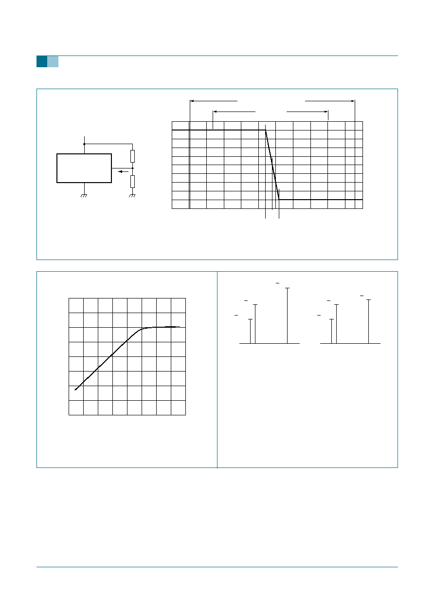
9397 750 13417
� Koninklijke Philips Electronics N.V. 2004. All rights reserved.
Product data sheet
Rev. 01 -- 16 November 2004
27 of 42
Philips Semiconductors
TDA9881
Alignment-free vision and FM sound IF PLL demodulator
Pin numbers for TDA9881HN in parenthesis.
Fig 9.
Typical analog AFC characteristic.
001aab345
0
5
4
3
2
1
36
37
38
40
41
38.9
38.71
39.09
lock range without SAW filter
f (MHz)
AFC window
V
AFC
(V)
+
200
+
100
0
-
100
I
AFC
(
�
A)
-
200
TDA9881
21
(23)
R1
22 k
R2
22 k
V
P
V
AFC
I
AFC
SC is sound carrier, with respect to sync level.
CC is chrominance carrier, with respect to sync
level.
PC is picture carrier, with respect to sync level.
The sound carrier levels are taking into account a
sound shelf attenuation of 14 dB (SAW filter
G1984M).
Fig 10. Typical signal-to-noise ratio as a function of VIF
input voltage.
Fig 11. Input signal conditions.
0
30
50
110
80
60
20
40
mhc112
70
90
V
i(VIF)
(dB
�
V)
S/N
(dB)
SC CC
PC
SC CC
PC
BLUE
YELLOW
21 dB
13.2 dB
3.2 dB
21 dB
13.2 dB
10 dB
mha739
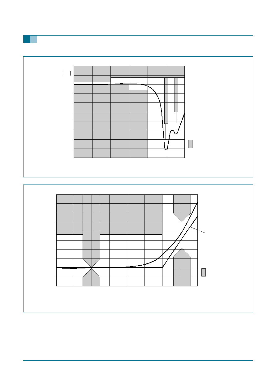
9397 750 13417
� Koninklijke Philips Electronics N.V. 2004. All rights reserved.
Product data sheet
Rev. 01 -- 16 November 2004
28 of 42
Philips Semiconductors
TDA9881
Alignment-free vision and FM sound IF PLL demodulator
Fig 12. Typical amplitude response for sound trap at M/N standard (inclusive Korea).
mhc122
-
40
2
2.5
3
3.5
4
4.5
5
-
30
-
20
-
10
0
10
f (MHz)
H(s)
(dB)
minimum
requirements
Overall delay is not shown, here the maximum ripple is specified.
Fig 13. Typical group delay for sound trap at M/N standard.
mhb167
-
100
0
0.5
1.5
2
3
1
2.5
3.5
4
0
100
200
300
400
f (MHz)
group
delay
(ns)
ideal characteristic
due to pre-correction
in the transmitter
minimum
requirements

9397 750 13417
� Koninklijke Philips Electronics N.V. 2004. All rights reserved.
Product data sheet
Rev. 01 -- 16 November 2004
29 of 42
Philips Semiconductors
TDA9881
Alignment-free vision and FM sound IF PLL demodulator
Fig 14. Typical amplitude response for sound trap at B/G standard.
mhb168
-
40
4
4.5
5
5.5
6
6.5
7
-
30
-
20
-
10
0
10
f (MHz)
H(s)
(dB)
minimum
requirements
Overall delay is not shown, here the maximum ripple is specified.
Fig 15. Typical group delay for sound trap at B/G standard.
mhb169
-
100
0
0.5
1.5
2
3
1
2.5
3.5
4
4.5
5
0
100
200
300
400
f (MHz)
group
delay
(ns)
ideal characteristic
due to pre-correction
in the transmitter
minimum
requirements
9397 750 13417
� Koninklijke Philips Electronics N.V. 2004. All rights reserved.
Product data sheet
Rev. 01 -- 16 November 2004
30 of 42
Philips Semiconductors
TDA9881
Alignment-free vision and FM sound IF PLL demodulator
Fig 16. Typical amplitude response for sound trap at I standard.
Fig 17. Typical amplitude response for sound trap at D/K standard.
mhc123
-
40
4
4.5
5
5.5
6
6.5
7
-
30
-
20
-
10
0
10
f (MHz)
H(s)
(dB)
minimum
requirements
mhb171
-
40
4
4.5
5
5.5
6
6.5
7
-
30
-
20
-
10
0
10
f (MHz)
H(s)
(dB)
minimum
requirements

9397 750 13417
� Koninklijke Philips Electronics N.V. 2004. All rights reserved.
Product data sheet
Rev. 01 -- 16 November 2004
31 of 42
Philips Semiconductors
TDA9881
Alignment-free vision and FM sound IF PLL demodulator
Conditions: PC/SC ratio is measured at pins VIF1 and VIF2; via transformer; 27 kHz FM deviation; 50
�
s de-emphasis.
(1) Signal.
(2) Noise at H-picture (CCIR weighted quasi peak).
(3) Noise at black picture (CCIR weighted quasi peak).
Fig 18. Audio signal-to-noise ratio as a function of picture-to-sound carrier ratio in intercarrier mode.
4
10
0
-
70
49
52
46
43
40
13
37
10
7
28
22
25
19
31
34
16
mhc118
-
50
-
30
-
20
-
10
-
40
-
60
S/N
W
(dB)
(1)
(2)
(3)
gain controlled operation of FM PLL
PC/SC ratio
9397 750 13417
� Koninklijke Philips Electronics N.V. 2004. All rights reserved.
Product data sheet
Rev. 01 -- 16 November 2004
32 of 42
Philips Semiconductors
TDA9881
Alignment-free vision and FM sound IF PLL demodulator
(1) Depends on TOP.
Fig 19. Front-end level diagram.
video 2 V (p-p)
0.66
�
10
-
3
0.66
�
10
-
5
001aab343
20
40
60
80
100
antenna input
(dB
�
V)
120
140
10
VHF/UHF tuner
VIF
VIF amplifier, demodulator
and video
tuner
SAW filter
TDA9881
IF signals
RMS value
(V)
10
-
1
10
-
2
(TOP)
10
-
3
10
-
4
10
-
5
1
10
(1)
SAW insertion
loss 20 dB
SAW insertion
loss 20 dB
tuning gain
control range
40 dB
RF gain
70 dB
VIF AGC
IF slip
6 dB
xxxx xxxxxxxxxxxxxxxxxxxxxxxxxxxxxx x xxxxxxxxxxxxxx xxxxxxxxxx xxx xxxxxx xxxxxxxxxxxxxxxxxxxxxxx xxxxxxxxxxxxxxxxxxxxxx
xxxxx xxxxxx xx xxxxxxxxxxxxxxxxxxxxxxxxxxxxx xxxxxxxxxxxxxxxxxxxxxx xxxxxxxxxxx xxxxxxx xxxxxxxxxxxxxxxxxxx
xxxxxxxxxxxxxxxx xxxxxxxxxxxxxx xxxxxx xx xxxxxxxxxxxxxxxxxxxxxxxxxxxxxxxx xxxxxxxxxxxxxxxxxxxxxxxx xxxxxxx
xxxxxxxxxxxxxxxxxxxxxxxxxxxxxxxxxxxxxxxxxxxxxx xxxxxxxxxxx xxxxx x x
9397 750 13417
� K
oninklijk
e Philips Electronics N.V
. 2004. All r
ights reser
v
ed.
Pr
oduct data sheet
Re
v
.
01 -- 16 No
vember 2004
33 of 42
Philips Semiconductor
s
TD
A9881
Alignment-free vision and FM sound IF PLL demodulator
12.
Application inf
ormation
Pin numbers for TDA9881HN in parenthesis.
(1) Optional measures to improve ESD performance within a TV-set application.
(2) Internal connected; the pin must be left open-circuit.
(3) AF output signal reduction; see
Table note 19
of
Section 11
.
Fig 20. Application diagram of TDA9881.
mhc503
47
�
F
10
�
F
(1)
5 V
5 V
470 nF
390
pF
10 nF
VIF1
VIF2
SIF2
SIF1
i.c.
(2)
FMPLL
AFC
VPLL
VP
AGND
DEEM
AFD
DGND
FMSO
FM0
QSSO
TOP
FM1
1.5
nF
tuner AGC
fref
BC847
CVBS output
TAGC
VIF0
CVBS
VAGC
REF
5.6 k
10 nF
12 k
100 k
220
330
75
220 nF
10 nF
100 pF
single
reference
QSS output
FM sound
output
TDA9881
51
1
2
5
4
3
IF
input
SAW
FILTER
G3962
1
2
5
4
3
SAW
FILTER
K9350
22 k
2.2 k
22 k
100 nF
22 k
Rx
(3)
n.c.
VIF1
AMUTE0
1 nF
(30)
1
22
(24)
23
(26)
18
(20)
21
(23)
20
(22)
19
(21)
17
(18)
16
(17)
15
(16)
14
(15)
13
(14)
24
(27)
(1)
3
(5)
7
(31)
2
(2)
4
(3)
5
(4)
6
(7)
8
(8)
9
(9)
10
(10)
11
(11)
12
xxxx xxxxxxxxxxxxxxxxxxxxxxxxxxxxxx x xxxxxxxxxxxxxx xxxxxxxxxx xxx xxxxxx xxxxxxxxxxxxxxxxxxxxxxx xxxxxxxxxxxxxxxxxxxxxx
xxxxx xxxxxx xx xxxxxxxxxxxxxxxxxxxxxxxxxxxxx xxxxxxxxxxxxxxxxxxxxxx xxxxxxxxxxx xxxxxxx xxxxxxxxxxxxxxxxxxx
xxxxxxxxxxxxxxxx xxxxxxxxxxxxxx xxxxxx xx xxxxxxxxxxxxxxxxxxxxxxxxxxxxxxxx xxxxxxxxxxxxxxxxxxxxxxxx xxxxxxx
xxxxxxxxxxxxxxxxxxxxxxxxxxxxxxxxxxxxxxxxxxxxxx xxxxxxxxxxx xxxxx x x
9397 750 13417
� K
oninklijk
e Philips Electronics N.V
. 2004. All r
ights reser
v
ed.
Pr
oduct data sheet
Re
v
.
01 -- 16 No
vember 2004
34 of 42
Philips Semiconductor
s
TD
A9881
Alignment-free vision and FM sound IF PLL demodulator
13.
T
est inf
ormation
Pin numbers for TDA9881HN in parenthesis.
(1) Different VIF loop filter in comparison with the application circuit due to different input characteristics (SAW filter or transformer).
(2) Internal connected; the pin must be left open-circuit.
(3) AF output signal reduction; see
Table note 19
of
Section 11
.
Fig 21. Test circuit.
(30)
1
22
(24)
23
(26)
18
(20)
21
(23)
20
(22)
19
(21)
17
(18)
16
(17)
15
(16)
14
(15)
13
(14)
external
reference
AFC
output
VIF PLL
filter
(1)
V
P
4 MHz
24
(27)
470 nF
390
pF
10 nF
22 k
VIF1
VIF2
SIF2
SIF1
i.c.
(2)
FMPLL
AFC
VPLL
V
P
AGND
DEEM
AFD
DGND
FMSO
FM0
QSSO
TOP
FM1
100
nF
1.5
nF
tuner AGC
output
CVBS
output
TAGC
VIF0
CVBS
VAGC
REF
5.6 k
10 nF
FM PLL
filter
22
k
22 k
150
220 nF
Cx
FM sound
output
single
reference
QSS output
TDA9881
51
1 : 1
VIF
input
51
1 : 1
SIF
input
n.c.
or
V
P
V
P
or
n.c.
n.c.
VIF1
V
P
or
n.c.
Rx
(3)
mhc505
2.2 k
AMUTE0
100
pF
n.c.
or
V
P
1 nF
(1)
3
(5)
7
(31)
2
(2)
4
(3)
5
(4)
6
(7)
8
(8)
9
(9)
10
(10)
11
(11)
12
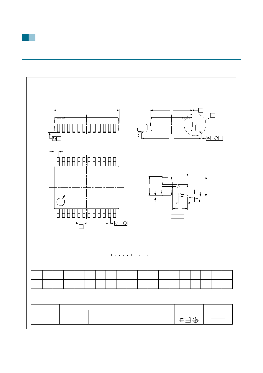
9397 750 13417
� Koninklijke Philips Electronics N.V. 2004. All rights reserved.
Product data sheet
Rev. 01 -- 16 November 2004
35 of 42
Philips Semiconductors
TDA9881
Alignment-free vision and FM sound IF PLL demodulator
14. Package outline
Fig 22. Package outline SOT340-1 (SSOP24).
UNIT
A
1
A
2
A
3
b
p
c
D
(1)
E
(1)
(1)
e
H
E
L
L
p
Q
Z
y
w
v
REFERENCES
OUTLINE
VERSION
EUROPEAN
PROJECTION
ISSUE DATE
IEC
JEDEC
JEITA
mm
0.21
0.05
1.80
1.65
0.38
0.25
0.20
0.09
8.4
8.0
5.4
5.2
0.65
1.25
7.9
7.6
0.9
0.7
0.8
0.4
8
0
o
o
0.13
0.1
0.2
DIMENSIONS (mm are the original dimensions)
Note
1. Plastic or metal protrusions of 0.2 mm maximum per side are not included.
1.03
0.63
SOT340-1
MO-150
99-12-27
03-02-19
X
w
M
A
A
1
A
2
b
p
D
H
E
L
p
Q
detail X
E
Z
e
c
L
v
M
A
(A )
3
A
1
12
24
13
0.25
y
pin 1 index
0
2.5
5 mm
scale
SSOP24: plastic shrink small outline package; 24 leads; body width 5.3 mm
SOT340-1
A
max.
2
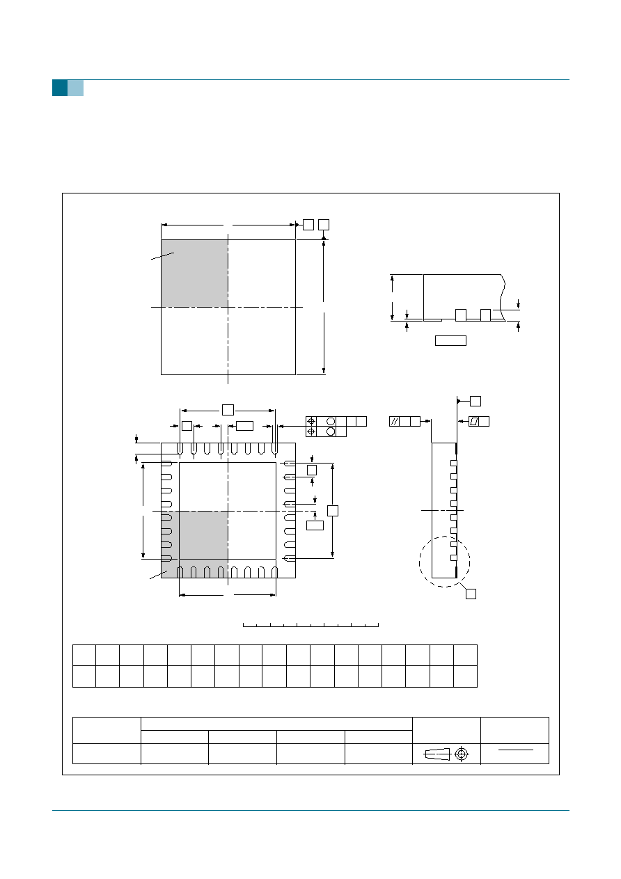
9397 750 13417
� Koninklijke Philips Electronics N.V. 2004. All rights reserved.
Product data sheet
Rev. 01 -- 16 November 2004
36 of 42
Philips Semiconductors
TDA9881
Alignment-free vision and FM sound IF PLL demodulator
Fig 23. Package outline SOT617-3 (HVQFN32).
terminal 1
index area
0.5
1
A1
Eh
b
UNIT
y
e
0.2
c
REFERENCES
OUTLINE
VERSION
EUROPEAN
PROJECTION
ISSUE DATE
IEC
JEDEC
JEITA
mm
5.1
4.9
Dh
3.75
3.45
y1
5.1
4.9
3.75
3.45
e1
3.5
e2
3.5
0.30
0.18
0.05
0.00
0.05
0.1
DIMENSIONS (mm are the original dimensions)
SOT617-3
MO-220
- - -
- - -
0.5
0.3
L
0.1
v
0.05
w
0
2.5
5 mm
scale
SOT617-3
HVQFN32: plastic thermal enhanced very thin quad flat package; no leads;
32 terminals; body 5 x 5 x 0.85 mm
A
(1)
max.
A
A1
c
detail X
y
y1 C
e
L
Eh
Dh
e
e1
b
9
16
32
25
24
17
8
1
X
D
E
C
B
A
e2
terminal 1
index area
02-04-18
02-10-22
1/2
e
1/2
e
A
C
C
B
v
M
w
M
E
(1)
Note
1. Plastic or metal protrusions of 0.075 mm maximum per side are not included.
D
(1)

9397 750 13417
� Koninklijke Philips Electronics N.V. 2004. All rights reserved.
Product data sheet
Rev. 01 -- 16 November 2004
37 of 42
Philips Semiconductors
TDA9881
Alignment-free vision and FM sound IF PLL demodulator
15. Soldering
15.1 Introduction to soldering surface mount packages
This text gives a very brief insight to a complex technology. A more in-depth account of
soldering ICs can be found in our
Data Handbook IC26; Integrated Circuit Packages
(document order number 9398 652 90011).
There is no soldering method that is ideal for all surface mount IC packages. Wave
soldering can still be used for certain surface mount ICs, but it is not suitable for fine pitch
SMDs. In these situations reflow soldering is recommended.
15.2 Reflow soldering
Reflow soldering requires solder paste (a suspension of fine solder particles, flux and
binding agent) to be applied to the printed-circuit board by screen printing, stencilling or
pressure-syringe dispensing before package placement. Driven by legislation and
environmental forces the worldwide use of lead-free solder pastes is increasing.
Several methods exist for reflowing; for example, convection or convection/infrared
heating in a conveyor type oven. Throughput times (preheating, soldering and cooling)
vary between 100 seconds and 200 seconds depending on heating method.
Typical reflow peak temperatures range from 215
�
C to 270
�
C depending on solder paste
material. The top-surface temperature of the packages should preferably be kept:
�
below 225
�
C (SnPb process) or below 245
�
C (Pb-free process)
� for all BGA, HTSSON..T and SSOP..T packages
� for packages with a thickness
2.5 mm
� for packages with a thickness < 2.5 mm and a volume
350 mm
3
so called
thick/large packages.
�
below 240
�
C (SnPb process) or below 260
�
C (Pb-free process) for packages with a
thickness < 2.5 mm and a volume < 350 mm
3
so called small/thin packages.
Moisture sensitivity precautions, as indicated on packing, must be respected at all times.
15.3 Wave soldering
Conventional single wave soldering is not recommended for surface mount devices
(SMDs) or printed-circuit boards with a high component density, as solder bridging and
non-wetting can present major problems.
To overcome these problems the double-wave soldering method was specifically
developed.
If wave soldering is used the following conditions must be observed for optimal results:
�
Use a double-wave soldering method comprising a turbulent wave with high upward
pressure followed by a smooth laminar wave.
�
For packages with leads on two sides and a pitch (e):
� larger than or equal to 1.27 mm, the footprint longitudinal axis is preferred to be
parallel to the transport direction of the printed-circuit board;

9397 750 13417
� Koninklijke Philips Electronics N.V. 2004. All rights reserved.
Product data sheet
Rev. 01 -- 16 November 2004
38 of 42
Philips Semiconductors
TDA9881
Alignment-free vision and FM sound IF PLL demodulator
� smaller than 1.27 mm, the footprint longitudinal axis must be parallel to the
transport direction of the printed-circuit board.
The footprint must incorporate solder thieves at the downstream end.
�
For packages with leads on four sides, the footprint must be placed at a 45
�
angle to
the transport direction of the printed-circuit board. The footprint must incorporate
solder thieves downstream and at the side corners.
During placement and before soldering, the package must be fixed with a droplet of
adhesive. The adhesive can be applied by screen printing, pin transfer or syringe
dispensing. The package can be soldered after the adhesive is cured.
Typical dwell time of the leads in the wave ranges from 3 seconds to 4 seconds at 250
�
C
or 265
�
C, depending on solder material applied, SnPb or Pb-free respectively.
A mildly-activated flux will eliminate the need for removal of corrosive residues in most
applications.
15.4 Manual soldering
Fix the component by first soldering two diagonally-opposite end leads. Use a low voltage
(24 V or less) soldering iron applied to the flat part of the lead. Contact time must be
limited to 10 seconds at up to 300
�
C.
When using a dedicated tool, all other leads can be soldered in one operation within
2 seconds to 5 seconds between 270
�
C and 320
�
C.
15.5 Package related soldering information
[1]
For more detailed information on the BGA packages refer to the
(LF)BGA Application Note (AN01026);
order a copy from your Philips Semiconductors sales office.
[2]
All surface mount (SMD) packages are moisture sensitive. Depending upon the moisture content, the
maximum temperature (with respect to time) and body size of the package, there is a risk that internal or
external package cracks may occur due to vaporization of the moisture in them (the so called popcorn
effect). For details, refer to the Drypack information in the
Data Handbook IC26; Integrated Circuit
Packages; Section: Packing Methods.
[3]
These transparent plastic packages are extremely sensitive to reflow soldering conditions and must on no
account be processed through more than one soldering cycle or subjected to infrared reflow soldering with
peak temperature exceeding 217
�
C
�
10
�
C measured in the atmosphere of the reflow oven. The package
body peak temperature must be kept as low as possible.
Table 13:
Suitability of surface mount IC packages for wave and reflow soldering methods
Package
[1]
Soldering method
Wave
Reflow
[2]
BGA, HTSSON..T
[3]
, LBGA, LFBGA, SQFP,
SSOP..T
[3]
, TFBGA, VFBGA, XSON
not suitable
suitable
DHVQFN, HBCC, HBGA, HLQFP, HSO, HSOP,
HSQFP, HSSON, HTQFP, HTSSOP, HVQFN,
HVSON, SMS
not suitable
[4]
suitable
PLCC
[5]
, SO, SOJ
suitable
suitable
LQFP, QFP, TQFP
not recommended
[5] [6]
suitable
SSOP, TSSOP, VSO, VSSOP
not recommended
[7]
suitable
CWQCCN..L
[8]
, PMFP
[9]
, WQCCN..L
[8]
not suitable
not suitable

9397 750 13417
� Koninklijke Philips Electronics N.V. 2004. All rights reserved.
Product data sheet
Rev. 01 -- 16 November 2004
39 of 42
Philips Semiconductors
TDA9881
Alignment-free vision and FM sound IF PLL demodulator
[4]
These packages are not suitable for wave soldering. On versions with the heatsink on the bottom side, the
solder cannot penetrate between the printed-circuit board and the heatsink. On versions with the heatsink
on the top side, the solder might be deposited on the heatsink surface.
[5]
If wave soldering is considered, then the package must be placed at a 45
�
angle to the solder wave
direction. The package footprint must incorporate solder thieves downstream and at the side corners.
[6]
Wave soldering is suitable for LQFP, QFP and TQFP packages with a pitch (e) larger than 0.8 mm; it is
definitely not suitable for packages with a pitch (e) equal to or smaller than 0.65 mm.
[7]
Wave soldering is suitable for SSOP, TSSOP, VSO and VSSOP packages with a pitch (e) equal to or larger
than 0.65 mm; it is definitely not suitable for packages with a pitch (e) equal to or smaller than 0.5 mm.
[8]
Image sensor packages in principle should not be soldered. They are mounted in sockets or delivered
pre-mounted on flex foil. However, the image sensor package can be mounted by the client on a flex foil by
using a hot bar soldering process. The appropriate soldering profile can be provided on request.
[9]
Hot bar soldering or manual soldering is suitable for PMFP packages.

9397 750 13417
� Koninklijke Philips Electronics N.V. 2004. All rights reserved.
Product data sheet
Rev. 01 -- 16 November 2004
40 of 42
Philips Semiconductors
TDA9881
Alignment-free vision and FM sound IF PLL demodulator
16. Revision history
Table 14:
Revision history
Document ID
Release date
Data sheet status
Change notice
Doc. number
Supersedes
TDA9881_1
20041116
Product data sheet
-
9397 750 13417
-

Philips Semiconductors
TDA9881
Alignment-free vision and FM sound IF PLL demodulator
9397 750 13417
� Koninklijke Philips Electronics N.V. 2004. All rights reserved.
Product data sheet
Rev. 01 -- 16 November 2004
41 of 42
17. Data sheet status
[1]
Please consult the most recently issued data sheet before initiating or completing a design.
[2]
The product status of the device(s) described in this data sheet may have changed since this data sheet was published. The latest information is available on the Internet at
URL http://www.semiconductors.philips.com.
[3]
For data sheets describing multiple type numbers, the highest-level product status determines the data sheet status.
18. Definitions
Short-form specification -- The data in a short-form specification is
extracted from a full data sheet with the same type number and title. For
detailed information see the relevant data sheet or data handbook.
Limiting values definition -- Limiting values given are in accordance with
the Absolute Maximum Rating System (IEC 60134). Stress above one or
more of the limiting values may cause permanent damage to the device.
These are stress ratings only and operation of the device at these or at any
other conditions above those given in the Characteristics sections of the
specification is not implied. Exposure to limiting values for extended periods
may affect device reliability.
Application information -- Applications that are described herein for any
of these products are for illustrative purposes only. Philips Semiconductors
make no representation or warranty that such applications will be suitable for
the specified use without further testing or modification.
19. Disclaimers
Life support -- These products are not designed for use in life support
appliances, devices, or systems where malfunction of these products can
reasonably be expected to result in personal injury. Philips Semiconductors
customers using or selling these products for use in such applications do so
at their own risk and agree to fully indemnify Philips Semiconductors for any
damages resulting from such application.
Right to make changes -- Philips Semiconductors reserves the right to
make changes in the products - including circuits, standard cells, and/or
software - described or contained herein in order to improve design and/or
performance. When the product is in full production (status `Production'),
relevant changes will be communicated via a Customer Product/Process
Change Notification (CPCN). Philips Semiconductors assumes no
responsibility or liability for the use of any of these products, conveys no
license or title under any patent, copyright, or mask work right to these
products, and makes no representations or warranties that these products are
free from patent, copyright, or mask work right infringement, unless otherwise
specified.
20. Contact information
For additional information, please visit: http://www.semiconductors.philips.com
For sales office addresses, send an email to: sales.addresses@www.semiconductors.philips.com
Level
Data sheet status
[1]
Product status
[2] [3]
Definition
I
Objective data
Development
This data sheet contains data from the objective specification for product development. Philips
Semiconductors reserves the right to change the specification in any manner without notice.
II
Preliminary data
Qualification
This data sheet contains data from the preliminary specification. Supplementary data will be published
at a later date. Philips Semiconductors reserves the right to change the specification without notice, in
order to improve the design and supply the best possible product.
III
Product data
Production
This data sheet contains data from the product specification. Philips Semiconductors reserves the
right to make changes at any time in order to improve the design, manufacturing and supply. Relevant
changes will be communicated via a Customer Product/Process Change Notification (CPCN).

� Koninklijke Philips Electronics N.V. 2004
All rights are reserved. Reproduction in whole or in part is prohibited without the prior
written consent of the copyright owner. The information presented in this document does
not form part of any quotation or contract, is believed to be accurate and reliable and may
be changed without notice. No liability will be accepted by the publisher for any
consequence of its use. Publication thereof does not convey nor imply any license under
patent- or other industrial or intellectual property rights.
Date of release: 16 November 2004
Document number: 9397 750 13417
Published in The Netherlands
Philips Semiconductors
TDA9881
Alignment-free vision and FM sound IF PLL demodulator
21. Contents
1
General description . . . . . . . . . . . . . . . . . . . . . . 1
2
Features . . . . . . . . . . . . . . . . . . . . . . . . . . . . . . . 1
3
Applications . . . . . . . . . . . . . . . . . . . . . . . . . . . . 1
4
Quick reference data . . . . . . . . . . . . . . . . . . . . . 2
5
Ordering information . . . . . . . . . . . . . . . . . . . . . 3
6
Block diagram . . . . . . . . . . . . . . . . . . . . . . . . . . 4
7
Pinning information . . . . . . . . . . . . . . . . . . . . . . 5
7.1
Pinning . . . . . . . . . . . . . . . . . . . . . . . . . . . . . . . 5
7.2
Pin description . . . . . . . . . . . . . . . . . . . . . . . . . 6
8
Functional description . . . . . . . . . . . . . . . . . . . 7
8.1
VIF amplifier . . . . . . . . . . . . . . . . . . . . . . . . . . . 7
8.2
Tuner AGC and VIF AGC . . . . . . . . . . . . . . . . . 7
8.3
VIF AGC detector . . . . . . . . . . . . . . . . . . . . . . . 7
8.4
FPLL detector . . . . . . . . . . . . . . . . . . . . . . . . . . 8
8.5
VCO and divider . . . . . . . . . . . . . . . . . . . . . . . . 8
8.6
AFC and digital acquisition help circuit . . . . . . . 8
8.7
Video demodulator and amplifier . . . . . . . . . . . 9
8.8
Sound carrier trap . . . . . . . . . . . . . . . . . . . . . . . 9
8.9
SIF amplifier . . . . . . . . . . . . . . . . . . . . . . . . . . . 9
8.10
SIF AGC detector . . . . . . . . . . . . . . . . . . . . . . . 9
8.11
Single reference QSS mixer . . . . . . . . . . . . . . 10
8.12
FM demodulator and acquisition help circuit . 10
8.13
Audio amplifier and mute time constant . . . . . 11
8.14
Internal voltage stabilizer . . . . . . . . . . . . . . . . 11
8.15
Logic . . . . . . . . . . . . . . . . . . . . . . . . . . . . . . . . 11
9
Limiting values. . . . . . . . . . . . . . . . . . . . . . . . . 12
10
Thermal characteristics. . . . . . . . . . . . . . . . . . 13
11
Characteristics . . . . . . . . . . . . . . . . . . . . . . . . . 13
12
Application information. . . . . . . . . . . . . . . . . . 33
13
Test information . . . . . . . . . . . . . . . . . . . . . . . . 34
14
Package outline . . . . . . . . . . . . . . . . . . . . . . . . 35
15
Soldering . . . . . . . . . . . . . . . . . . . . . . . . . . . . . 37
15.1
Introduction to soldering surface mount
packages . . . . . . . . . . . . . . . . . . . . . . . . . . . . 37
15.2
Reflow soldering . . . . . . . . . . . . . . . . . . . . . . . 37
15.3
Wave soldering . . . . . . . . . . . . . . . . . . . . . . . . 37
15.4
Manual soldering . . . . . . . . . . . . . . . . . . . . . . 38
15.5
Package related soldering information . . . . . . 38
16
Revision history . . . . . . . . . . . . . . . . . . . . . . . . 40
17
Data sheet status . . . . . . . . . . . . . . . . . . . . . . . 41
18
Definitions . . . . . . . . . . . . . . . . . . . . . . . . . . . . 41
19
Disclaimers . . . . . . . . . . . . . . . . . . . . . . . . . . . . 41
20
Contact information . . . . . . . . . . . . . . . . . . . . 41