 | –≠–ª–µ–∫—Ç—Ä–æ–Ω–Ω—ã–π –∫–æ–º–ø–æ–Ω–µ–Ω—Ç: TEA0679 | –°–∫–∞—á–∞—Ç—å:  PDF PDF  ZIP ZIP |

DATA SHEET
Product specification
Supersedes data of 1998 Jun 24
File under Integrated Circuits, IC01
1998 Nov 12
INTEGRATED CIRCUITS
TEA0679T
I
2
C-bus controlled dual Dolby*
B-type noise reduction circuit for
playback applications

1998 Nov 12
2
Philips Semiconductors
Product specification
I
2
C-bus controlled dual Dolby* B-type noise
reduction circuit for playback applications
TEA0679T
FEATURES
∑
Dual Noise Reduction (NR) channels
∑
Head preamplifiers
∑
Reverse head switching
∑
Automatic Music Search (AMS)
∑
Blank skip
∑
Mute position
∑
Equalization with electronically switched time constants
∑
Switch functions and level adjustment controlled via
I
2
C-bus
∑
Optional switch inputs TTL compatible
∑
Dolby reference level = 387.5 mV
∑
Contained in a 32-pin small outline package
∑
Improved EMC behaviour.
GENERAL DESCRIPTION
The TEA0679T is a bipolar integrated circuit that provides
two channels of Dolby B noise reduction for playback
applications in car radios. It includes head and
equalization amplifiers with electronically switchable time
constants. The device also includes electronically
switchable inputs for tape drivers with reverse heads.
This device detects pauses of music in the Automatic
Music Search (AMS) scan mode (for applications with an
intelligent controlled tape driver) or AMS latch mode (for
applications with a simple controlled tape driver).
For both modes the delay time can be fixed by using an
external resistor. In the blank skip mode the IC can detect
pauses of music during playback and allows a
microcontroller to react on this situation.
The equalization amplifier gain adjustment, the output
offset adjustment and all switching functions are I
2
C-bus
controlled. Head switching and equalization time constant
switching can be controlled via separate pins (optional).
The device operates with power supplies from 7.6 to 12 V.
The output overload level increases with increases in
supply voltage.
Current drain varies with the following variables:
∑
Supply voltage
∑
Noise reduction on/off
∑
AMS on/off.
Because of this current drain variation it is advisable to use
a regulated power supply or a supply with a long time
constant.
QUICK REFERENCE DATA
ORDERING INFORMATION
Remark Dolby*: Available only to licensees of Dolby Laboratories Licensing Corporation, San Francisco, CA94111,
USA, from whom licensing and application information must be obtained. Dolby is a registered trade-mark of Dolby
Laboratories Licensing Corporation.
SYMBOL
PARAMETER
MIN.
TYP.
MAX.
UNIT
V
CC
supply voltage
7.6
-
12
V
I
CC
supply current
-
35
40
mA
signal plus noise-to-noise ratio
78
84
-
dB
TYPE
NUMBER
PACKAGE
NAME
DESCRIPTION
VERSION
TEA0679T
SO32
plastic small outline package; 32 leads; body width 7.5 mm
SOT287-1
S
N
+
N
--------------
1998
Nov
12
3
Philips Semiconductors
Product specification
I
2
C-bus controlled dual Dolby* B-type noise
reduction circuit for playback applications
TEA0679T
This text is here in white to force landscape pages to be rotated correctly when browsing through the pdf in the Acrobat reader.This text is here in
_
white to force landscape pages to be rotated correctly when browsing through the pdf in the Acrobat reader.This text is here inThis text is here in
white to force landscape pages to be rotated correctly when browsing through the pdf in the Acrobat reader. white to force landscape pages to be ...
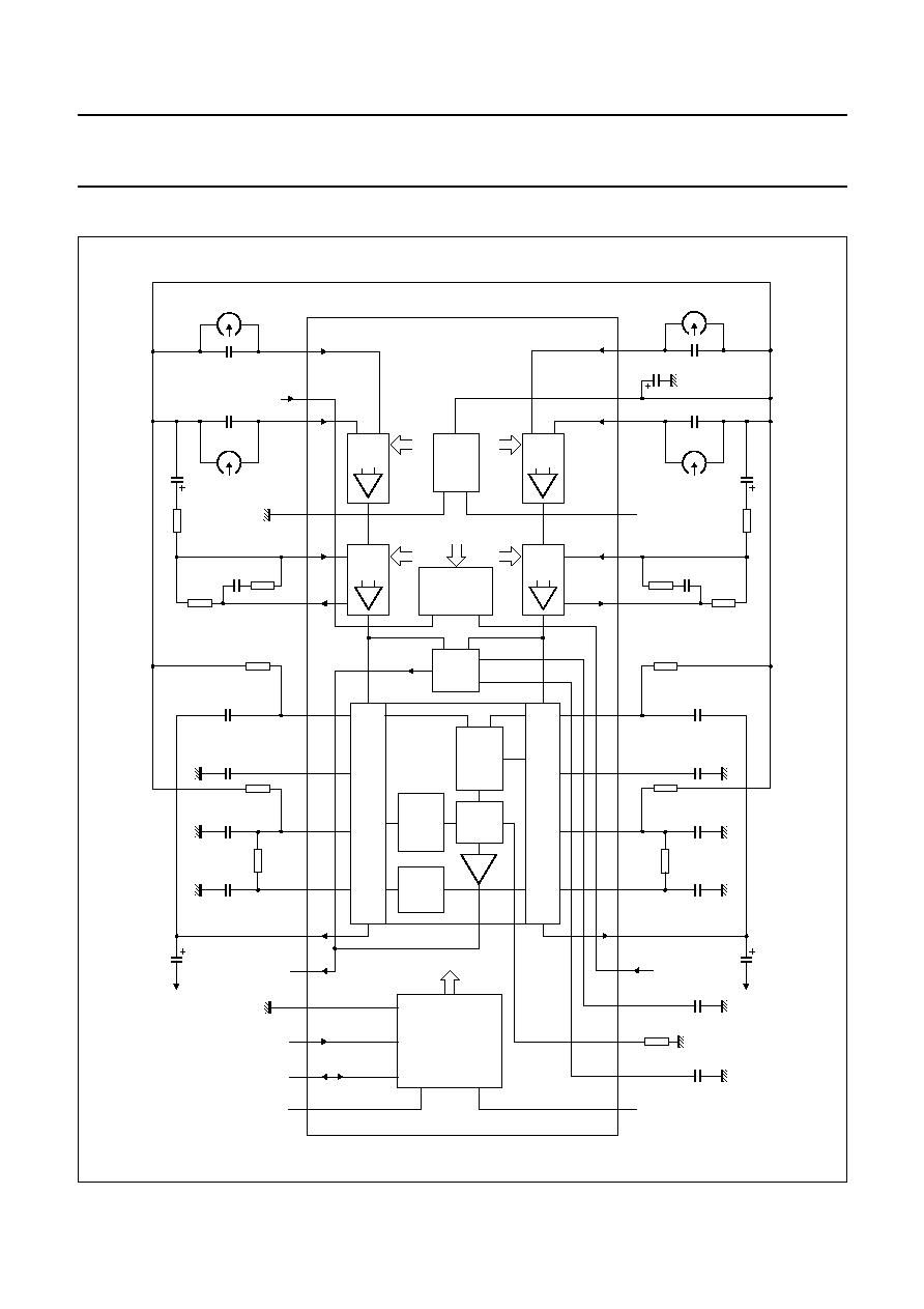
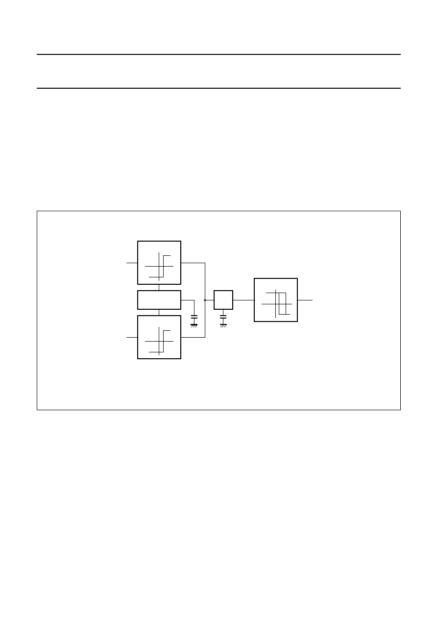
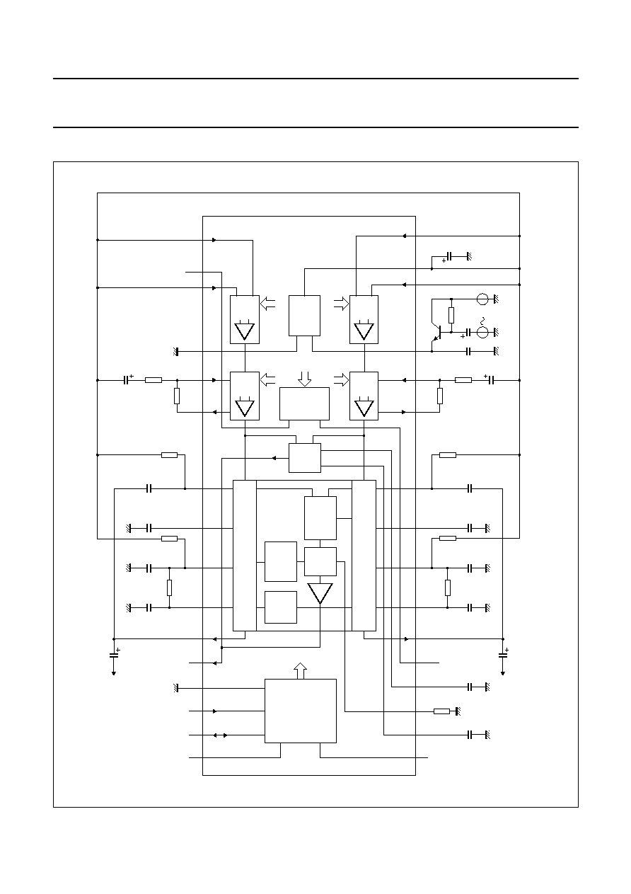
BLOCK DIAGRAM
handbook, full pagewidth
MHB117
I
2
C-BUS
PRE
AMP
LOGIC
EQ
AMP
13
VCC
PRE
AMP
EQ
AMP
POWER
SUPPLY
LEVEL
DETECTOR
DELAY
TIME
LATCH
AND
RISE TIME
AMS
PROCESSOR
MUTE
14
INA1
15
Vref
12
EQFA
11
EQA
16
INA2
DOLBY B
DOLBY B
20
AGND
BLANK
SKIP
19
INB1
18
HS
HS
(opt)
21
EQFB
22
EQB
17
INB2
TEA0679T
10
SCA
HPA
23
SCB
9
CONTRA
24
HPB
8
INTA
25
26
CONTRB
7
OUTA
27
INTB
6
5
EQS
EQS
(opt)
28
29
30
OUTB
DGND AMS
3
TD
SCL
2
BSC
31
SDA
1
MAD
32
BEN
4
BTC
output A
100
µ
F
470
pF
470
pF
4.7 nF
15 nF
2.7 k
10
µ
F
8.2
nF
5.6
k
24 k
(
±
2%)
Rt
(ref)
180 k
(
±
10%)
390 k
470
pF
470
pF
2.7 k
10
µ
F
8.2
nF
5.6
k
390 k
270 k
(
±
10%)
(
±
5%)
100 nF
(
±
10%)
47 nF
220 nF
330 nF
(
±
10%)
(
±
5%)
10
µ
F
output B
4.7 nF
(
±
5%)
15 nF
(
±
5%)
24 k
(
±
2%)
180 k
(
±
10%)
270 k
(
±
10%)
100 nF
(
±
10%)
330 nF
(
±
10%)
10
µ
F
Fig.1 Block and application diagram.
1998 Nov 12
4
Philips Semiconductors
Product specification
I
2
C-bus controlled dual Dolby* B-type noise
reduction circuit for playback applications
TEA0679T
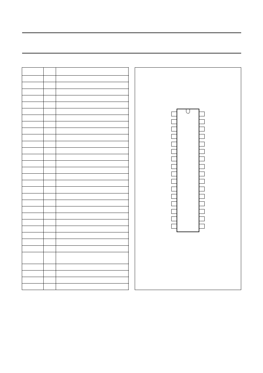
PINNING
SYMBOL
PIN
DESCRIPTION
MAD
1
programmable address bit
BSC
2
blank skip reference capacitance
TD
3
delay time constant
BTC
4
blank skip integration capacitance
EQS
5
equalization switch input (optional)
OUTA
6
output channel A
INTA
7
integrating filter channel A
CONTRA
8
control voltage channel A
HPA
9
high-pass filter channel A
SCA
10
side chain channel A
EQA
11
equalizing output channel A
EQFA
12
equalizing input channel A
V
CC
13
supply voltage
INA1
14
input channel A1 (forward or reverse)
V
ref
15
reference voltage
INA2
16
input channel A2 (reverse or forward)
INB2
17
input channel B2 (reverse or forward)
HS
18
head switch input (optional)
INB1
19
input channel B1 (forward or reverse)
AGND
20
analog ground
EQFB
21
equalizing input channel B
EQB
22
equalizing output channel B
SCB
23
side chain channel B
HPB
24
high-pass filter channel B
CONTRB
25
control voltage channel B
INTB
26
integrating filter channel B
OUTB
27
output channel B
AMS
28
Automatic Music Search (AMS)
output
DGND
29
digital ground
SCL
30
serial clock input
SDA
31
serial data input/output
BEN
32
bus enable
Fig.2 Pin configuration.
handbook, halfpage
TEA0679T
MHB118
1
2
3
4
5
6
7
8
9
10
11
12
13
14
15
16
32
31
30
29
28
27
26
25
24
23
22
21
20
19
18
17
MAD
BSC
TD
BTC
EQS
OUTA
INTA
CONTRA
HPA
SCA
EQA
EQFA
VCC
INA1
BEN
SDA
SCL
DGND
OUTB
INTB
AMS
CONTRB
HPB
SCB
EQB
EQFB
AGND
INB1
Vref
INA2
HS
INB2

1998 Nov 12
5
Philips Semiconductors
Product specification
I
2
C-bus controlled dual Dolby* B-type noise
reduction circuit for playback applications
TEA0679T
FUNCTIONAL DESCRIPTION
The following functions can be controlled via the I
2
C-bus:
∑
Equalization time constant switching
∑
Head switching
∑
Automatic Music Search (AMS) modes and blank skip
∑
Noise Reduction (NR) on/off switching
∑
Mute switching
∑
Equalization amplifier gain adjustment
∑
Output offset adjustment.
Dolby B noise reduction only operates correctly if the 0 dB
Dolby level is adjusted at 387.5 mV. The gain adjustment
can also be used to change the AMS level detector
threshold. The IC is able to generate an internal power-on
reset to guarantee a proper start-up behaviour.
Two of the above functions can be controlled via separate
pins (optional), if required.
Head switching is achieved when pin HS is connected to a
LOW level (input IN2 active) or connected to a HIGH level
(input IN1 active).
Equalization time constant switching (70 or 120
µ
s) is
achieved when pin EQS is connected to a LOW level
(70
µ
s) or connected to a HIGH level (120
µ
s).
If I
2
C-bus control is used the respective external function
control pin has to be left open-circuit. When open-circuit
the current state of the function can be observed at these
pins.
Automatic Music Search (AMS) modes and blank skip
If AMS is active (search mode bits SMOD1 = 1 and
SMOD0 = 0 or 1) the NR function is internally switched off
and the equalization time constant is internally forced to
70
µ
s. The signals of both channels are full-wave rectified
and then added. This means that even if one channel
appears inverted to the other channel the normal AMS
function is ensured.
It is possible to choose between the AMS scan and the
AMS latch mode via the I
2
C-bus. Due to the usage of an
internal flip-flop the switching from one mode to the other
must be done via the AMS off state. This guarantees an
appropriate flip-flop reset:
∑
Start from the initial AMS off state (SMOD1 = 0 and
SMOD0 = 0 or 1)
∑
Enable the desired AMS operation mode: AMS latch
mode (SMOD1 = 1 and SMOD0 = 0) or AMS scan mode
(SMOD1 = 1 and SMOD0 = 1).
For further information on music search see Figs 4 to 8.
If blank skip is active (SMOD1 = 0 and SMOD0 = 1)
periods of music can be detected in the playback mode
using the AMS pin as the detector output. It is possible to
defeat this function via the I
2
C-bus (SMOD1 = 0 and
SMOD0 = 0). For further information on blank skip
see Figs 9 and 10.
Offset adjustment procedure
The offset adjustment is performed using two bits in the
I
2
C-bus write byte 0. The offset monitor bit OMOR enables
the AMS output to indicate whether the selected offset
value is positive or negative. The channel select bit OFCH
selects the channel (A or B) which is currently monitored
by the output at pin AMS. The monitoring needs a few
microseconds until the output result is valid. A complete
offset adjustment is performed in the following way:
∑
Adjust the output to Dolby level using the I
2
C-bus
controlled equalization gain adjustment
∑
Enable the offset monitor and select the channel to be
monitored by transmitting the bits OMOR = 1 and OFCH
(0 = Channel A, 1 = Channel B) to the IC
∑
If the monitor output (pin AMS) is LOW send the next
offset value OFFCHA or OFFCHB one offset step below
the last valid value. If the monitor output (pin AMS) is
HIGH send the next offset value OFFCHA or OFFCHB
one offset step above the last valid value
∑
Repeat the last two steps until the monitor output
changes its polarity
∑
If necessary store the transmitted digital offset value for
the selected channel.
The start value is either set by the power-on reset or the
last I
2
C-bus transmission. The offset adjustment can be
performed during the power-on reset condition and also
each time the tape driver is not active. A complete digital
offset data set consists of four values: one for each head
(head 1 and head 2) in each channel. After an offset value
transmission the IC stores one value for channel A and
one value for channel B. If a head switch is performed
these values have to be updated via the I
2
C-bus for the
alternative head.

1998 Nov 12
6
Philips Semiconductors
Product specification
I
2
C-bus controlled dual Dolby* B-type noise
reduction circuit for playback applications
TEA0679T
I
2
C-bus operation mode
The IC is capable of operating with I
2
C-bus systems that provide either 5 V or digital supply voltage related logic levels
below 5 V. This is achieved using the bus enable (pin 32) with different input voltages. An open pin or input voltages
above 5 V enable 5 V related I
2
C-bus logic levels. If input voltages between 3 and 5 V are used the IC operates with
I
2
C-bus logic levels related to these input voltages. To disable the I
2
C-bus receiver it is necessary to use pin voltages
below the specified LOW level.
LIMITING VALUES
In accordance with the Absolute Maximum Rating System (IEC 134).
Notes
1. The TEA0679T allows a HIGH level at switching pins without voltage (V
CC
= 0; standby mode). This means a
maximum input voltage of 6.5 V for the switching pins.
2. Human body model (1.5 k
; 100 pF).
3. Machine model (0
; 200 pF).
THERMAL CHARACTERISTICS
SYMBOL
PARAMETER
CONDITIONS
MIN.
MAX.
UNIT
V
CC
supply voltage
0
14
V
V
i
input voltage (pins 1 to 32) except pin 5 (EQS),
pin 15 (V
ref
), pin 18 (HS), pin 30 (SCL) and pin 31
(SDA) to V
CC
-
0.3
V
CC
V
V
i(n1)
input voltage at pin 30 (SCL) and pin 31 (SDA)
-
0.3
+12
V
V
i(n2)
input voltage at pin 5 (EQS) and pin 18 (HS)
-
0.3
+6.5
V
V
i(stb)
standby input voltage at pin 1 (MAD), pin 32 (BEN),
pin 5 (EQS) and pin 18 (HS)
note 1
-
0.3
+6.5
V
t
sc
pin 15 (V
ref
) to V
CC
short-circuiting duration
-
5
s
T
stg
storage temperature
-
55
+150
∞
C
T
amb
operating ambient temperature
-
40
+85
∞
C
V
es
electrostatic handling voltage for all pins
note 2
-
2
+2
kV
note 3
-
500
+500
V
SYMBOL
PARAMETER
CONDITIONS
VALUE
UNIT
R
th(j-a)
thermal resistance from junction to ambient
in free air
62
K/W

1998 Nov 12
7
Philips Semiconductors
Product specification
I
2
C-bus controlled dual Dolby* B-type noise
reduction circuit for playback applications
TEA0679T
CHARACTERISTICS
V
CC
= 10 V; f = 20 Hz to 20 kHz; T
amb
= 25
∞
C; all levels are referenced to V
o
= 387.5 mV (RMS) (0 dB) at test point
(TP) pin OUTA or OUTB; see Fig.1; NR on/AMS off; EQ switch in the 70
µ
s position; unless otherwise specified.
SYMBOL
PARAMETER
CONDITIONS
MIN.
TYP.
MAX.
UNIT
V
CC
supply voltage
7.6
10
12
V
I
CC
supply current
-
35
40
mA
m
channel matching
f = 1 kHz; V
o
= 0 dB; NR off
-
0.5
-
+
0.5
dB
THD
total harmonic distortion
(2nd and 3rd harmonic)
f = 1 kHz; V
o
= 0 dB
-
0.08
0.15
%
f = 10 kHz; V
o
= 10 dB
-
0.15
0.3
%
H
R
headroom at output
V
CC
= 7.6 V; THD = 1%;
f = 1 kHz
12
-
-
dB
signal plus noise-to-noise ratio
internal gain 40 dB, linear;
CCIR/ARM weighted;
decode mode; see Fig.41
78
84
-
dB
PSRR
power supply ripple rejection
V
i(rms)
= 0.25 V; f = 1 kHz;
see Fig.38
52
57
-
dB
V
o
output voltage frequency
response; referenced to TP
encode mode; see Fig.41
-
25 dB; f = 0.2 kHz
-
25.9
-
24.4
-
22.9
dB
0 dB; f = 1 kHz
-
1.5
0
+
1.5
dB
-
25 dB; f = 1 kHz
-
20.8
-
19.3
-
17.8
dB
-
25 dB; f = 5 kHz
-
21.1
-
19.6
-
18.1
dB
-
35 dB; f = 10 kHz
-
27.4
-
25.9
-
24.4
dB
cs
channel separation
V
o
= 10 dB; f = 1 kHz;
see Fig.39
57
63
-
dB
ct
crosstalk between active and
inactive input
f = 1 kHz; V
o
= 10 dB; NR off;
see Fig.39
70
77
-
dB
R
L
load resistance at output
AC-coupled; f = 1 kHz;
V
o
= 12 dB; THD = 1%
10
-
-
k
G
v
voltage gain of preamplifier
pin INA1/INA2 to pin EQFA;
pin INB1/INB2 to pin EQFB;
f = 1 kHz
29
30
31
dB
V
i(offset)(DC)
DC input offset voltage
-
2
-
mV
I
i(bias)
input bias current
-
0.1
0.4
µ
A
R
EQ
internal equalization resistor
pin EQA/EQB to EQ amplifier
A/B output
4.7
5.8
6.9
k
R
i
input resistance of head inputs
60
100
-
k
G
v(ol)
open-loop gain
pin INA1 or INA2 to pin EQA;
pin INB1 or INB2 to pin EQB;
additional gain = 0 dB
f = 10 kHz
80
86
-
dB
f = 400 Hz
104
110
-
dB
V
ref
-
V
OUT
DC output offset voltage at
pins OUTA and OUTB after
adjustment
NR off; pins INA1, INA2, INB1
and INB2 connected to V
ref
-
20
-
+
20
mV
S
N
+
N
--------------

1998 Nov 12
8
Philips Semiconductors
Product specification
I
2
C-bus controlled dual Dolby* B-type noise
reduction circuit for playback applications
TEA0679T
I
O
DC output current
pins OUTA and OUTB
connected to ground
-
2
-
-
mA
pins OUTA and OUTB
connected to V
CC
0.3
-
-
mA
Z
o
output impedance
-
80
100
V
no(rms)
equivalent input noise voltage
(RMS value)
NR off; unweighted;
f = 20 Hz to 20 kHz;
R
source
= 0
-
0.7
1.4
µ
V
V
TD
AMS timing (DC level)
resistor R
t
connected to pin TD V
CC
-
3
-
V
CC
V
V
offset(DC)
DC offset voltage at pins OUTA
and OUTB
f = 900 MHz; V
i(rms)
= 6 V
-
40
-
mV
V
offset(AD)
overall offset voltage between
AGND (pin 20) and DGND
(pin 29)
-
0.4
-
+0.4
V
Level adjustment
G
CR
gain control range
note 1
24.2
25.2
26.2
dB
G
step
step size
-
0.4
-
dB
G
E
step error between any
adjacent step
-
-
0.4
dB
Switching thresholds
O
PTIONAL EQUALIZATION TIME CONSTANT SWITCH
(pin EQS)
V
IL
LOW-level input voltage
70
µ
s; I
L
-
200
µ
A
-
0.3
-
+0.8
V
V
OL
LOW-level output voltage
70
µ
s; I
L
1 mA
-
-
0.4
V
V
IH
HIGH-level input voltage
120
µ
s
2
-
-
V
V
OH
HIGH-level output voltage
120
µ
s; I
L
-
50
µ
A
2.8
-
3.3
V
O
PTIONAL HEAD SWITCH
(pin HS)
V
IL
LOW-level input voltage
INPUT 2 on; I
L
-
150
µ
A
-
0.3
-
+0.8
V
V
OL
LOW-level output voltage
INPUT 2 on; I
L
10
µ
A
-
-
0.4
V
V
IH
HIGH-level input voltage
INPUT 1 on
2
-
-
V
V
OH
HIGH-level output voltage
INPUT 1 on; I
L
-
50
µ
A
2.8
-
3.3
V
Search modes
B
LANK SKIP
BS
th(M-P)
dynamic level threshold
blank skip mode; f = 10 kHz
-
30
-
27
-
24
dB
t
sw(P-M)
switching time pause-to-music
blank skip mode; f = 10 kHz;
signal on channel A and B;
note 2
2.1
4.15
6.3
ms
blank skip mode; f = 10 kHz;
signal on one channel; note 2
4.1
8.3
12.5
ms
t
sw(M-P)
switching time music-to-pause
blank skip mode; f = 10 kHz;
note 2
10
19
30
ms
SYMBOL
PARAMETER
CONDITIONS
MIN.
TYP.
MAX.
UNIT

1998 Nov 12
9
Philips Semiconductors
Product specification
I
2
C-bus controlled dual Dolby* B-type noise
reduction circuit for playback applications
TEA0679T
Notes
1. For Dolby NR level adjust and AMS pause detection level setting.
2. All blank skip timing characteristics are based on the assumption that a signal level change from
-
33 to
-
21 dB
pause-to-music or
-
21 to
-
33 dB music-to-pause occurs in the specified channels.
3. The high speed of the tape (FF and REW) at the tape head during AMS mode causes a transformation of level and
frequency of the originally recorded signal. It means a boost of signal level of approximately 10 dB and more for
recorded frequencies from 500 Hz to 4 kHz. So the threshold level of
-
22 dB corresponds to signal levels in PlayBack
(PB) mode of approximately
-
32 dB. The AMS inputs for each channel are pins SCA and SCB. As the frequency
spectrum is transformed by a factor of approximately 10 to 30 due to the higher tape speed in FF and REW, the
high-pass filter (4.7 nF/24 k
) removes the effect of offset voltages but does not affect the music search function.
In the block and application diagram (see Fig.1) the frequency response of the system between tape heads input,
e.g. pins INA2 and INB2, to the AMS input pins SCA and SCB is constant over the whole frequency range (see
Fig.3).
4. These levels correspond to a gain setting of Dolby level at TP (for TP see Fig.41). The gain adjustment can be used
to change the threshold level during AMS operation.
5. The characteristics are in accordance with the I
2
C-bus specification. Information about the I
2
C-bus can be found in
the brochure
"The I
2
C-bus and how to use it" (order number 9398 393 40011).
A
UTOMATIC
M
USIC
S
EARCH
(AMS)
t
W(min)(r)
minimum pulse width rise time
AMS scan mode
2
-
10
ms
AMS latch mode
130
-
170
ms
AMS
(P-M)
signal level at output for AMS
switching pause-to-music
AMS mode; f = 10 kHz;
notes 3 and 4; see Fig.40
-
23.7
-
21
-
18
dB
AMS
(M-P)
AMS switching hysteresis
music-to-pause
AMS mode; f = 10 kHz
-
0.7
-
1
-
1.3
dB
O
UTPUT
(pin AMS)
V
OH
HIGH-level output voltage
I
L
-
1 mA
2.8
-
3.3
V
V
OL
LOW-level output voltage
I
L
1 mA
-
-
0.4
V
Digital part (pins MAD and BEN)
V
IH
HIGH-level input voltage
3
-
V
CC
V
V
IL
LOW-level input voltage
-
0.3
-
+
1.5
V
I
IH
HIGH-level input current
-
10
-
+
10
µ
A
I
IL
LOW-level input current
-
10
-
+
10
µ
A
Digital part (pins SDA and SCL); note 4
V
IH
HIGH-level input voltage
BEN (pin 32) open-circuit
3
-
V
CC
V
5 V
V
BEN
V
CC
3
-
V
CC
V
3 V
V
BEN
< 5 V
0.7V
BEN
-
V
CC
V
V
IL
LOW-level input voltage
BEN (pin 32) open-circuit
-
0.3
-
+
1.5
V
5 V
V
BEN
V
CC
-
0.3
-
+
1.5
V
3 V
V
BEN
< 5 V
-
0.3
-
0.3V
BEN
V
I
IH
HIGH-level input current
V
CC
= 0 to 12 V
-
10
-
+
10
µ
A
I
IL
LOW-level input current
-
10
-
+
10
µ
A
V
OL
LOW-level output voltage SDA
I
L
= 3 mA
-
-
0.4
V
SYMBOL
PARAMETER
CONDITIONS
MIN.
TYP.
MAX.
UNIT
1998 Nov 12
10
Philips Semiconductors
Product specification
I
2
C-bus controlled dual Dolby* B-type noise
reduction circuit for playback applications
TEA0679T
General note
It is recommended to switch off V
CC
with a gradient of 400 V/s at maximum to avoid plops on tape in the event of contact
between tape and tape head while switching off.
AMS delay time
Table 1
AMS delay time set by resistor R
t
at pin TD
AMS threshold level
RESISTOR VALUE R
t
(k
)
DELAY TIME t
d
TYP. (ms)
TOLERANCE (%)
68
23
20
150
42
15
180
48
15
220
56
15
270
65
10
330
76
10
470
98
10
560
112
10
680
126
10
820
142
10
1000
160
10
Fig.3 AMS threshold level.
(1) AMS threshold level for application circuit (see Fig.1).
(2) AMS threshold level for test circuit (see Fig.40).
handbook, halfpage
-
20
-
60
-
40
-
30
-
50
MHB119
10
2
10
3
10
4
10
5
AMS(P-M)
(dB)
f (Hz)
(1)
(2)

1998 Nov 12
11
Philips Semiconductors
Product specification
I
2
C-bus controlled dual Dolby* B-type noise
reduction circuit for playback applications
TEA0679T
Short description of music search
A system for music search consists mainly of a level and a
time detection circuit (see Fig.4). For adapting and
decoupling the input signal is amplified (A), then rectified
(B) and smoothed with a time constant (C). Thus the
voltage at (C) corresponds to the signal level and will be
compared to the predefined pause level at the first
comparator (D), the level detector. If the signal level
becomes smaller than the pause level, the level detector
changes its output signal. Due to the output level of the
level detector the capacitor of the second time constant (E)
will be charged, respectively discharged.
If the pause level of the input signal remains for a certain
time period, the voltage at the capacitor reaches a certain
value, which corresponds to an equivalent time value.
The voltage at the capacitor will be compared to a
predefined time-equivalent voltage by the second
comparator (F), the time detector. If the pause level of the
input signal remains for this predefined time, the time
detector changes its output level to pause found status.
Fig.4 Integrated music search function.
handbook, full pagewidth
MED624
COMPARATOR 1
COMPARATOR 2
t1
t2
INPUT
AMPLIFIER
RECTIFIER
(A)
(B)
(C)
(D)
(E)
(F)
OUTPUT
Vt
VI
LEVEL DETECTOR
TIME DETECTOR

1998 Nov 12
12
Philips Semiconductors
Product specification
I
2
C-bus controlled dual Dolby* B-type noise
reduction circuit for playback applications
TEA0679T
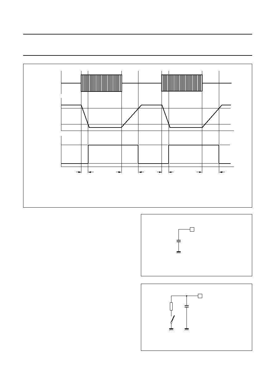
Description of the principle timing diagram for AMS
scan mode without initial input signal (see Fig.5)
By activating the AMS scan mode the AMS output level
directly indicates whether the input level corresponds to a
pause level (V
AMSEQ
= LOW) or not (V
AMSEQ
= HIGH).
At t
0
the AMS scan mode is activated. Without a signal at
V
in
, the following initial procedure runs until the AMS
output changes to a LOW level: due to no signal at V
in
the
voltage at the level detector input V
I
(CONTRA) remains
below the level threshold and the second time constant will
be discharged (time detector input V
t
). When V
t
exceeds
the time threshold level, the time detector output changes
to LOW level. Now the initial procedure is completed.
If a signal burst appears at t
3
, the level detector input
voltage rises immediately and causes its output to charge
the second time constant, which supplies the input voltage
V
t
for the time detector.
When V
t
exceeds the upper threshold level after the rise
time t
r
(at t
4
) the AMS output changes to HIGH. If the signal
burst ends at t
5
the level detector input V
I
falls to its LOW
level. Discharging of the second time constant begins
when the level threshold is exceeded at t
6
. The circuit then
measures the delay time t
d
, which is externally fixed by a
resistor and defines the length of a pause to be detected.
If no signal appears at V
in
within the time interval t
d
, the
time detector output switches the AMS output to a LOW
level at t
7
.
If a plop noise pulse appears at V
in
(t
8
) with a pulse width
less than the rise time t
r
> t
b
, the plop noise will not be
detected as music. The AMS output remains LOW.
Similarly the system handles no music pulses t
p
: when
music appears at t
11
with a small interruption at t
13
, this
interruption will not affect the AMS output for t
p
< t
d
.
Fig.5 AMS scan mode without initial input signal.
handbook, full pagewidth
MHB120
output signal
to microprocessor
4.5 V
VAMSEQ
time threshold
upper threshold
(hysteresis)
Vt
Vref
level threshold
Vl
Vin
Vl: voltage at
level detector
input
pin 8 (CONTRA)
Vt: voltage at
time detector
input
pin 25 (CONTRB)
t
t
t
t
AMS on
tr
td
tf
tb
<
tr
tp
<
td
t0
t3 t4
t5 t6
t7
t8 t9 t10
t11 t12
t13 t14
t15
t
r
= rise time; t
d
= delay time; t
b
= burst time; t
p
= pause time; t
f
= fall time.
1998 Nov 12
13
Philips Semiconductors
Product specification
I
2
C-bus controlled dual Dolby* B-type noise
reduction circuit for playback applications
TEA0679T
Description of the principle timing diagram for AMS scan mode with initial input signal (see Fig.6)
The AMS scan mode is activated at t
0
. With an input signal at V
in
, the following initial procedure runs until the circuit gets
a steady state status.
Due to the signal at V
in
the voltage at the level detector input V
I
(CONTRA) slides to a value which is defined by a limiter.
This voltage causes the level detector output to charge the second time constant (time detector input V
t
) to its maximum
voltage level at t
1
. The initial procedure is now completed.
The following behaviour does not differ from the description in Section "Description of the principle timing diagram for
AMS scan mode without initial input signal (see Fig.5)".
Fig.6 AMS scan mode with initial input signal.
handbook, full pagewidth
MHB121
output signal
to microprocessor
4.5 V
VAMSEQ
time threshold
upper threshold
(hysteresis)
Vt
Vref
level threshold
Vl
Vin
Vl: voltage at
level detector
input
pin 8 (CONTRA)
Vt: voltage at
time detector
input
pin 25 (CONTRB)
t
t
t
t
AMS on
td
tf
tb
<
tr
tp
<
tr
t0 t1
t5 t6
t7 t8 t9 t10
t11 t12
t13 t14
t15
t
r
= rise time; t
d
= delay time; t
b
= burst time; t
p
= pause time; t
f
= fall time.

1998 Nov 12
14
Philips Semiconductors
Product specification
I
2
C-bus controlled dual Dolby* B-type noise
reduction circuit for playback applications
TEA0679T
Description of the principle timing diagram for AMS
latch mode without initial input signal (see Fig.7)
This is similar to the description of the principle timing
diagram from AMS scan mode. It only differs in its initial
behaviour and its rise time t
r
(it should be noted that the
different t
r
does not occur in the principle timing diagrams
for latch and scan mode).
Running in AMS latch mode, the circuit may be simply
applied to drive a stop solenoid via a power FET. So a
further processing of the AMS output signal is not
necessary. Because there is no processor to make a
decision whether there is plop noise or not, for this mode
the rise time t
r
is extended to approximately 150 ms.
By activating the AMS latch mode the AMS output will not
change to a LOW level at t
0
if there is no initial signal at V
in
.
A latch forces the AMS output to remain HIGH until a
signal appears at V
in
(t
4
). After t
4
the latch will not affect the
output until the AMS latch mode is started again.
The existence of the latch appears necessary if the AMS
output, for example, drives a stop solenoid via a power
FET. The LOW output level will cause a drive of the stop
solenoid. This will happen after a maximum time of t
d
occurs without any input signal. If there is no music on tape
for a long time (e.g. at tape end), the AMS mode will be
activated repeatedly as long as there is no signal at V
in
.
Thus the circuit waits until music appears before detecting
the pauses.
Fig.7 AMS latch mode without initial input signal.
handbook, full pagewidth
MHB122
output signal
to power FET
4.5 V
VAMSEQ
time threshold
upper threshold
(hysteresis)
Vt
Vref
level threshold
Vl
Vin
Vl: voltage at
level detector
input
pin 8 (CONTRA)
Vt: voltage at
time detector
input
pin 25 (CONTRB)
t
t
t
t
internal
latch status
H
L
t
AMS on
tr
td
tf
tb
<
tr
tp
<
td
t0
t3 t4
t5 t6
t7
t8 t9 t10
t11 t12
t13 t14
t15
t
r
= rise time; t
d
= delay time; t
b
= burst time; t
p
= pause time; t
f
= fall time.

1998 Nov 12
15
Philips Semiconductors
Product specification
I
2
C-bus controlled dual Dolby* B-type noise
reduction circuit for playback applications
TEA0679T
Description of the principle timing diagram for AMS latch mode with initial input signal (see Fig.8)
This is similar to the description in Section "Description of the principle timing diagram for AMS scan mode with initial
input signal (see Fig.6)". It only differs in its rise time t
r
and a release of its internal latch when voltage V
t
exceeds the
upper threshold between t
0
and t
1
. The initial procedure is now completed.
The following behaviour does not differ from the description in Section "Description of the principle timing diagram for
AMS latch mode without initial input signal (see Fig.7)".
Fig.8 AMS latch mode with initial input signal.
handbook, full pagewidth
MHB123
output signal
to power FET
4.5 V
VAMSEQ
time threshold
upper threshold
(hysteresis)
Vt
Vref
level threshold
Vl
Vin
Vl: voltage at
level detector
input
pin 8 (CONTRA)
Vt: voltage at
time detector
input
pin 25 (CONTRB)
t
t
t
t
internal
latch status
L
H
t
AMS on
td
tf
tb
<
tr
tp
<
td
t0 t1
t5 t6
t7 t8 t9 t10
t11 t12
t13 t14
t15
t
r
= rise time; t
d
= delay time; t
b
= burst time; t
p
= pause time; t
f
= fall time.
1998 Nov 12
16
Philips Semiconductors
Product specification
I
2
C-bus controlled dual Dolby* B-type noise
reduction circuit for playback applications
TEA0679T
Short description of blank skip
The blank skip system is intended to detect pauses of
music during playback mode. It consists of two input signal
level comparators, an integration capacitor and an output
comparator with hysteresis. The DC voltage of the inputs
A and B, increased by the level threshold value, is used as
the reference voltage for the input comparators. If input
A or B exceeds this voltage the integration capacitor is
discharged. If this voltage falls below the lower threshold
the output comparator changes its polarity to the music
found status.
In the event that none of the two inputs A or B exceeds the
level threshold the integration capacitor is charged. After
its voltage has exceeded the upper threshold of the output
comparator the output changes its polarity to the pause
found status.
It is recommended to process the output signal with a
microcontroller to perform, for example, spike suppression
for a certain time.
Fig.9 Integrated blank skip function.
(1) V
C
: integration capacitor voltage.
handbook, full pagewidth
MHB124
COMPARATOR
COMPARATOR
REFERENCE
VOLTAGE
t1
INPUT A
COMPARATOR
OUTPUT
INPUT B
VC
(1)
1998 Nov 12
17
Philips Semiconductors
Product specification
I
2
C-bus controlled dual Dolby* B-type noise
reduction circuit for playback applications
TEA0679T
Fig.10 Blank skip timing diagram.
V
C
; integration capacitor voltage: t
sw(P-M)
; switching time pause-to-music: t
sw(M-P)
; switching time music-to-pause.
handbook, full pagewidth
lower threshold
upper threshold
INPUT
VC
t
t
VLOW
VHIGH
OUTPUT
t
tsw(P-M)
tsw(P-M)
tsw(M-P)
tsw(M-P)
MHB125
Soft head switching
In general the head switching procedure is recommended
to be performed in four steps:
1. Activate the mute function
2. Switch to the alternative head
3. Adjust the offset for the new head
4. Deactivate the mute function.
In applications without a mute function a soft head switch
via the I
2
C-bus can be realized using a capacitor
connected to pin 18. A proposal for this switching
mechanism is shown in Fig.11. To guarantee the internal
timing for the head switching operation an externally
connected device to pin 18 should not modify the output
current significantly.
An additional resistor is necessary if the head switching is
performed externally via the optional switching input
capability at pin 18. A proposal for this kind of switching is
shown in Fig.12.
In general soft head switching is only suitable if equal
offset values for head 1 and head 2 exist. A soft offset
value switching is not possible with the TEA0679T.
Fig.11 Soft head switching via the I
2
C-bus.
handbook, halfpage
MHB126
10
µ
F
pin 18
HS (optional)
Fig.12 External soft head switching.
handbook, halfpage
MHB127
8 k
10
µ
F
IN2
IN1
pin 18
HS (optional)

1998 Nov 12
18
Philips Semiconductors
Product specification
I
2
C-bus controlled dual Dolby* B-type noise
reduction circuit for playback applications
TEA0679T
I
2
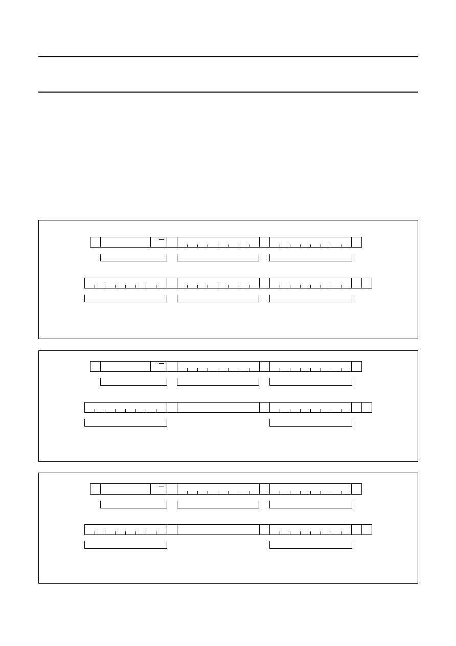
C-BUS PROTOCOL
I
2
C-bus format
Table 2
Explanation of I
2
C-bus format to read (slave transmits data)
Table 3
Write byte 0; SELECT
S
SLAVE ADDRESS
A
DATA
A
P
NAME
DESCRIPTION
S
START condition
SLAVE ADDRESS
101 100 00 (MAD = LOW)
101 100 10 (MAD = HIGH)
A
acknowledge; generated by the slave
DATA
see Tables 3 to 10
P
STOP condition
FUNCTIONS
BITS OF DATA BYTE SELECT
MSB
LSB
SMOD1
SMOD0
HSW
MUTE
NROF
OFCH
OMOR
EQT
Equalization time constant
70
µ
s
-
-
-
-
-
-
-
0
120
µ
s
-
-
-
-
-
-
-
1
Offset monitor
AMS output
-
-
-
-
-
-
0
-
offset monitor
-
-
-
-
-
-
1
-
Offset channel
channel A
-
-
-
-
-
0
-
-
channel B
-
-
-
-
-
1
-
-
NR on/off
on
-
-
-
-
0
-
-
-
off
-
-
-
-
1
-
-
-
Mute off/on
off
-
-
-
0
-
-
-
-
on
-
-
-
1
-
-
-
-
Head switch
IN2
-
-
0
-
-
-
-
-
IN1
-
-
1
-
-
-
-
-
Search mode
off
0
0
-
-
-
-
-
-
blank skip
0
1
-
-
-
-
-
-
AMS latch mode
1
0
-
-
-
-
-
-
AMS scan mode
1
1
-
-
-
-
-
-

1998 Nov 12
19
Philips Semiconductors
Product specification
I
2
C-bus controlled dual Dolby* B-type noise
reduction circuit for playback applications
TEA0679T
Table 4
Write byte 1; EQADJA
ADDITIONAL GAIN
POSITIONS (dB)
BITS OF DATA BYTE EQADJA
MSB
LSB
NOT USED NOT USED
EQA5
EQA4
EQA3
EQA2
EQA1
EQA0
0
0
0
0
0
0
0
0
0
0.4
0
0
0
0
0
0
0
1
0.8
0
0
0
0
0
0
1
0
1.2
0
0
0
0
0
0
1
1
1.6
0
0
0
0
0
1
0
0
2.0
0
0
0
0
0
1
0
1
2.4
0
0
0
0
0
1
1
0
2.8
0
0
0
0
0
1
1
1
3.2
0
0
0
0
1
0
0
0
3.6
0
0
0
0
1
0
0
1
4.0
0
0
0
0
1
0
1
0
4.4
0
0
0
0
1
0
1
1
4.8
0
0
0
0
1
1
0
0
5.2
0
0
0
0
1
1
0
1
5.6
0
0
0
0
1
1
1
0
6.0
0
0
0
0
1
1
1
1
6.4
0
0
0
1
0
0
0
0
6.8
0
0
0
1
0
0
0
1
7.2
0
0
0
1
0
0
1
0
7.6
0
0
0
1
0
0
1
1
8.0
0
0
0
1
0
1
0
0
8.4
0
0
0
1
0
1
0
1
8.8
0
0
0
1
0
1
1
0
9.2
0
0
0
1
0
1
1
1
9.6
0
0
0
1
1
0
0
0
10.0
0
0
0
1
1
0
0
1
10.4
0
0
0
1
1
0
1
0
10.8
0
0
0
1
1
0
1
1
11.2
0
0
0
1
1
1
0
0
11.6
0
0
0
1
1
1
0
1
12.0
0
0
0
1
1
1
1
0
12.4
0
0
0
1
1
1
1
1
12.8
0
0
1
0
0
0
0
0
13.2
0
0
1
0
0
0
0
1
13.6
0
0
1
0
0
0
1
0
14.0
0
0
1
0
0
0
1
1
14.4
0
0
1
0
0
1
0
0

1998 Nov 12
20
Philips Semiconductors
Product specification
I
2
C-bus controlled dual Dolby* B-type noise
reduction circuit for playback applications
TEA0679T
14.8
0
0
1
0
0
1
0
1
15.2
0
0
1
0
0
1
1
0
15.6
0
0
1
0
0
1
1
1
16.0
0
0
1
0
1
0
0
0
16.4
0
0
1
0
1
0
0
1
16.8
0
0
1
0
1
0
1
0
17.2
0
0
1
0
1
0
1
1
17.6
0
0
1
0
1
1
0
0
18.0
0
0
1
0
1
1
0
1
18.4
0
0
1
0
1
1
1
0
18.8
0
0
1
0
1
1
1
1
19.2
0
0
1
1
0
0
0
0
19.6
0
0
1
1
0
0
0
1
20.0
0
0
1
1
0
0
1
0
20.4
0
0
1
1
0
0
1
1
20.8
0
0
1
1
0
1
0
0
21.2
0
0
1
1
0
1
0
1
21.6
0
0
1
1
0
1
1
0
22.0
0
0
1
1
0
1
1
1
22.4
0
0
1
1
1
0
0
0
22.8
0
0
1
1
1
0
0
1
23.2
0
0
1
1
1
0
1
0
23.6
0
0
1
1
1
0
1
1
24.0
0
0
1
1
1
1
0
0
24.4
0
0
1
1
1
1
0
1
24.8
0
0
1
1
1
1
1
0
25.2
0
0
1
1
1
1
1
1
ADDITIONAL GAIN
POSITIONS (dB)
BITS OF DATA BYTE EQADJA
MSB
LSB
NOT USED NOT USED
EQA5
EQA4
EQA3
EQA2
EQA1
EQA0

1998 Nov 12
21
Philips Semiconductors
Product specification
I
2
C-bus controlled dual Dolby* B-type noise
reduction circuit for playback applications
TEA0679T
Table 5
Write byte 2; EQADJB
ADDITIONAL GAIN
POSITIONS (dB)
BITS OF DATA BYTE EQADJB
MSB
LSB
NOT USED NOT USED
EQB5
EQB4
EQB3
EQB2
EQB1
EQB0
0
0
0
0
0
0
0
0
0
0.4
0
0
0
0
0
0
0
1
0.8
0
0
0
0
0
0
1
0
1.2
0
0
0
0
0
0
1
1
1.6
0
0
0
0
0
1
0
0
2.0
0
0
0
0
0
1
0
1
2.4
0
0
0
0
0
1
1
0
2.8
0
0
0
0
0
1
1
1
3.2
0
0
0
0
1
0
0
0
3.6
0
0
0
0
1
0
0
1
4.0
0
0
0
0
1
0
1
0
4.4
0
0
0
0
1
0
1
1
4.8
0
0
0
0
1
1
0
0
5.2
0
0
0
0
1
1
0
1
5.6
0
0
0
0
1
1
1
0
6.0
0
0
0
0
1
1
1
1
6.4
0
0
0
1
0
0
0
0
6.8
0
0
0
1
0
0
0
1
7.2
0
0
0
1
0
0
1
0
7.6
0
0
0
1
0
0
1
1
8.0
0
0
0
1
0
1
0
0
8.4
0
0
0
1
0
1
0
1
8.8
0
0
0
1
0
1
1
0
9.2
0
0
0
1
0
1
1
1
9.6
0
0
0
1
1
0
0
0
10.0
0
0
0
1
1
0
0
1
10.4
0
0
0
1
1
0
1
0
10.8
0
0
0
1
1
0
1
1
11.2
0
0
0
1
1
1
0
0
11.6
0
0
0
1
1
1
0
1
12.0
0
0
0
1
1
1
1
0
12.4
0
0
0
1
1
1
1
1
12.8
0
0
1
0
0
0
0
0
13.2
0
0
1
0
0
0
0
1
13.6
0
0
1
0
0
0
1
0
14.0
0
0
1
0
0
0
1
1
14.4
0
0
1
0
0
1
0
0

1998 Nov 12
22
Philips Semiconductors
Product specification
I
2
C-bus controlled dual Dolby* B-type noise
reduction circuit for playback applications
TEA0679T
Table 6
Write byte 3; OFFCHA
14.8
0
0
1
0
0
1
0
1
15.2
0
0
1
0
0
1
1
0
15.6
0
0
1
0
0
1
1
1
16.0
0
0
1
0
1
0
0
0
16.4
0
0
1
0
1
0
0
1
16.8
0
0
1
0
1
0
1
0
17.2
0
0
1
0
1
0
1
1
17.6
0
0
1
0
1
1
0
0
18.0
0
0
1
0
1
1
0
1
18.4
0
0
1
0
1
1
1
0
18.8
0
0
1
0
1
1
1
1
19.2
0
0
1
1
0
0
0
0
19.6
0
0
1
1
0
0
0
1
20.0
0
0
1
1
0
0
1
0
20.4
0
0
1
1
0
0
1
1
20.8
0
0
1
1
0
1
0
0
21.2
0
0
1
1
0
1
0
1
21.6
0
0
1
1
0
1
1
0
22.0
0
0
1
1
0
1
1
1
22.4
0
0
1
1
1
0
0
0
22.8
0
0
1
1
1
0
0
1
23.2
0
0
1
1
1
0
1
0
23.6
0
0
1
1
1
0
1
1
24.0
0
0
1
1
1
1
0
0
24.4
0
0
1
1
1
1
0
1
24.8
0
0
1
1
1
1
1
0
25.2
0
0
1
1
1
1
1
1
OFFSET CHANNEL A
POSITIONS
BITS OF DATA BYTE OFFCHA
MSB
LSB
OFA7
OFA6
OFA5
OFA4
OFA3
OFA2
OFA1
OFA0
Maximum positive
0
0
0
0
0
0
0
0
...
...
...
...
...
...
...
...
Maximum negative
1
1
1
1
1
1
1
1
ADDITIONAL GAIN
POSITIONS (dB)
BITS OF DATA BYTE EQADJB
MSB
LSB
NOT USED NOT USED
EQB5
EQB4
EQB3
EQB2
EQB1
EQB0
1998 Nov 12
23
Philips Semiconductors
Product specification
I
2
C-bus controlled dual Dolby* B-type noise
reduction circuit for playback applications
TEA0679T
Table 7
Write byte 4; OFFCHB
Table 8
Optionally pin controlled switch functions
Table 9
MAD switch
Table 10 BEN switch
OFFSET CHANNEL B
POSITIONS
BITS OF DATA BYTE OFFCHB
MSB
LSB
OFB7
OFB6
OFB5
OFB4
OFB3
OFB2
OFB1
OFB0
Maximum positive
0
0
0
0
0
0
0
0
...
...
...
...
...
...
...
...
Maximum negative
1
1
1
1
1
1
1
1
FUNCTIONS
HS (PIN 18)
EQS (PIN 5)
PIN STATE
DATA BIT
HSW
PIN STATE
DATA BIT
EQT
OUTPUT
INPUT
OUTPUT
INPUT
Equalization time constant
70
µ
s
-
-
-
LOW
open-circuit
0
120
µ
s
-
-
-
HIGH
open-circuit
1
70
µ
s
-
-
-
LOW
LOW
-
Head switch
IN2
LOW
open-circuit
0
-
-
-
IN1
HIGH
open-circuit
1
-
-
-
IN2
LOW
LOW
-
-
-
-
MODULE ADDRESS
MAD (PIN 1)
101 100 10
open-circuit
101 100 10
HIGH
101 100 00
LOW
I
2
C-BUS OPERATION MODE
BEN (PIN 32)
Active; 5 V thresholds
open-circuit
Active; 5 V thresholds
HIGH (5 V to V
CC
)
Active; V
BEN
related thresholds
HIGH (3 to 5 V)
Inactive
LOW
1998 Nov 12
24
Philips Semiconductors
Product specification
I
2
C-bus controlled dual Dolby* B-type noise
reduction circuit for playback applications
TEA0679T
I
2
C-bus transmission types
The I
2
C-bus format depends on the kind of data which
should be transmitted. To speed up the offset adjustment
procedure three types of transmissions from master to
slave are possible. The transmission type is controlled by
bits OFCH and OMOR in write byte 0.
If the OMOR bit is set to logic 0 the standard transmission
type is used. The corresponding byte sequence is shown
in Fig.13. This kind of transmission should by used for
changes in the IC settings during normal operation.
If the OMOR bit is set to logic 1 and the OFCH bit is set to
logic 0 the transmission type for an offset adjust in
channel A is selected. The byte sequence is shown in
Fig.14. During this kind of transmission the pin AMS is
used as the offset monitor output for channel A.
If the OMOR bit is set to logic 1 and the OFCH bit is set to
logic 1 the transmission type for an offset adjust in
channel B is selected. The byte sequence is shown in
Fig.15. During this kind of transmission the pin AMS is
used as the offset monitor output for channel B.
Fig.13 Standard transmission.
handbook, full pagewidth
MHB128
A
S
CHIP ADDRESS
A
A
X
0
R/W
ADDRESS
BYTE 0
BYTE 1
A
P
A
A
BYTE 2
BYTE 3
BYTE 4
Fig.14 Offset adjust channel A transmission.
handbook, full pagewidth
MHB129
A
S
CHIP ADDRESS
A
A
0
1
R/W
ADDRESS
BYTE 0
BYTE 3
A
P
A
A
BYTE 3
BYTE 3
Fig.15 Offset adjust channel B transmission.
handbook, full pagewidth
MHB130
A
S
CHIP ADDRESS
A
A
1
1
R/W
ADDRESS
BYTE 0
BYTE 4
A
P
A
A
BYTE 4
BYTE 4
1998 Nov 12
25
Philips Semiconductors
Product specification
I
2
C-bus controlled dual Dolby* B-type noise
reduction circuit for playback applications
TEA0679T
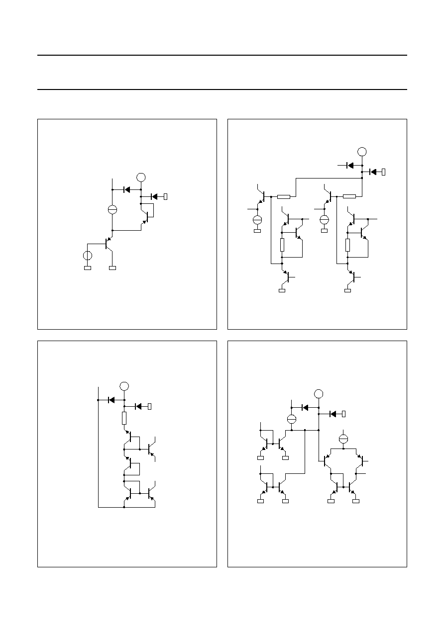
INTERNAL PIN CONFIGURATIONS
Fig.16 Pin 1: programmable address bit.
handbook, halfpage
MHB131
1
+
1.6 V
Fig.17 Pin 2: blank skip reference capacitance.
handbook, halfpage
2
+
80 k
160
80 k
160
MHB132
Fig.18 Pin 3: delay time constant.
handbook, halfpage
MHB133
3
+
8 V
1 k
Fig.19 Pin 4: blank skip integration capacitance.
handbook, halfpage
MHB134
4
+

1998 Nov 12
26
Philips Semiconductors
Product specification
I
2
C-bus controlled dual Dolby* B-type noise
reduction circuit for playback applications
TEA0679T
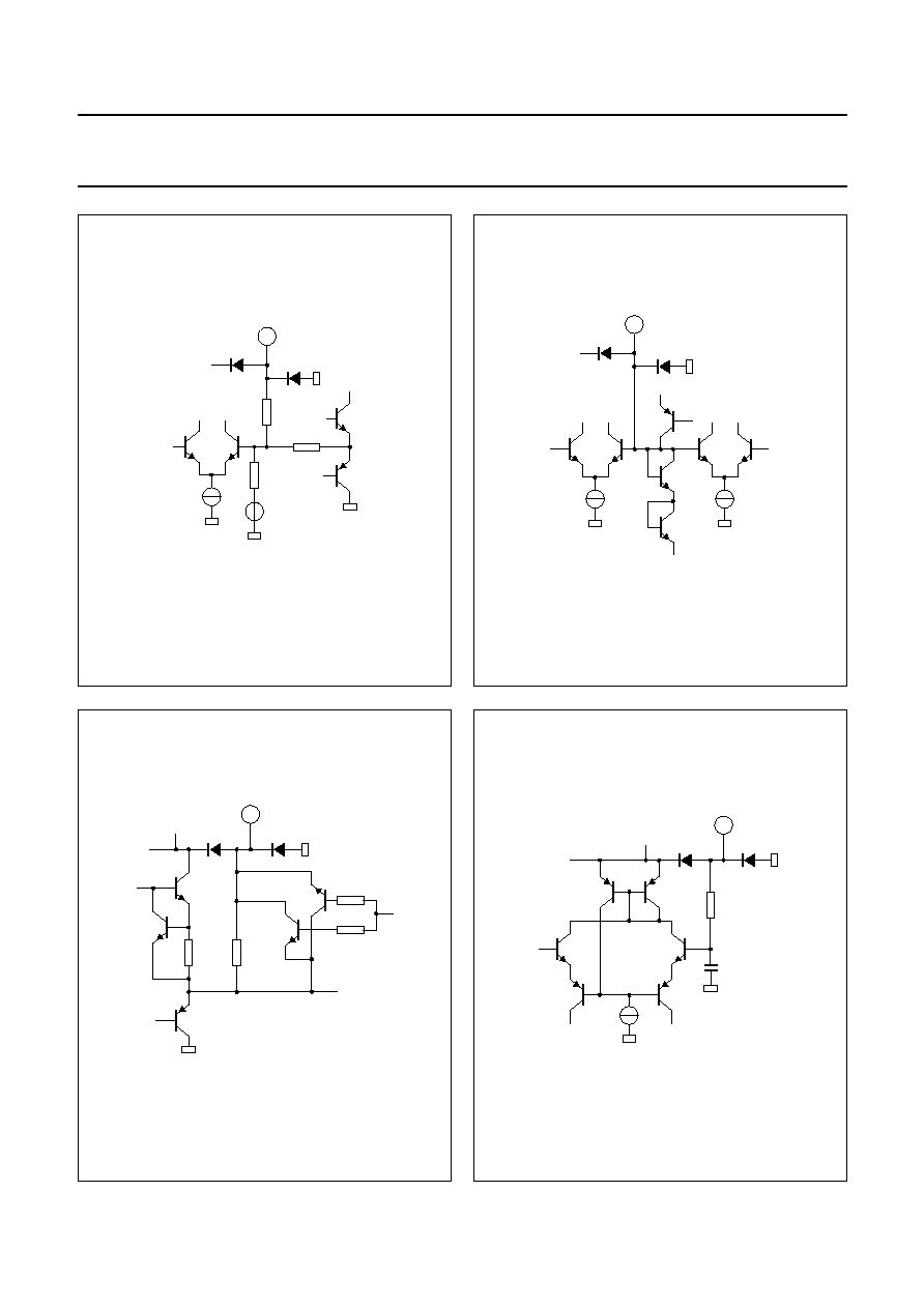
Fig.20 Pin 5: EQ switch input.
handbook, halfpage
MHB135
5
+
3 V
Fig.21 Pins 6 and 27: output channel.
handbook, halfpage
MHB136
6
+
5 V
85
85
47
Fig.22 Pin 7: integrating filter channel A.
handbook, halfpage
MHB137
7
+
Vref
±
0.23 V
3.6 k
Fig.23 Pin 8: control voltage channel A.
handbook, halfpage
MHB138
8
+
5 V
1.2 k
3.4 k
3.6 k
40 k
5 V
1998 Nov 12
27
Philips Semiconductors
Product specification
I
2
C-bus controlled dual Dolby* B-type noise
reduction circuit for playback applications
TEA0679T
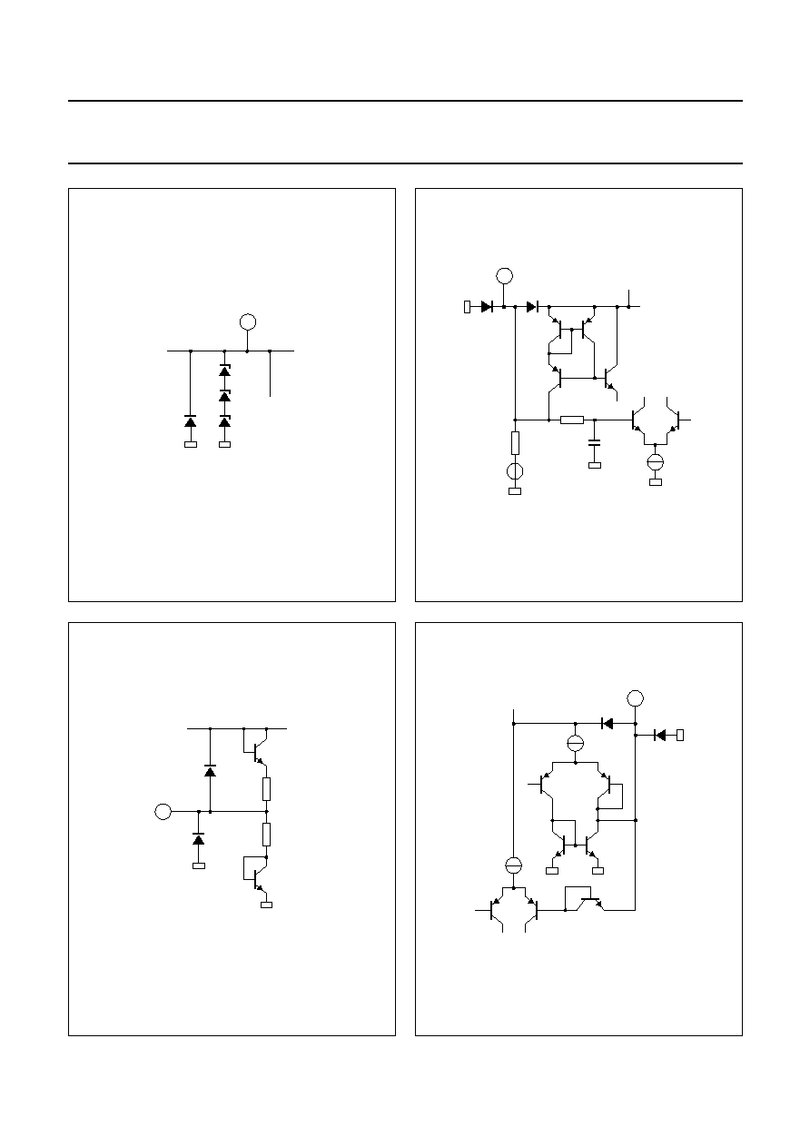
Fig.24 Pins 9 and 24: high-pass filter.
handbook, halfpage
MHB139
9
+
+
5 V
5 V
9 k
9 k
670
Fig.25 Pins 10 and 23: side chain.
handbook, halfpage
MHB140
10
+
5 V
Fig.26 Pins 11 and 22: equalizing output.
handbook, halfpage
MHB141
11
+
5 V
160
5.8 k
20 k
20 k
Fig.27 Pins 12 and 21: equalizing input.
handbook, halfpage
MHB142
12
+
5 V
2.7 pF
10 k
1998 Nov 12
28
Philips Semiconductors
Product specification
I
2
C-bus controlled dual Dolby* B-type noise
reduction circuit for playback applications
TEA0679T
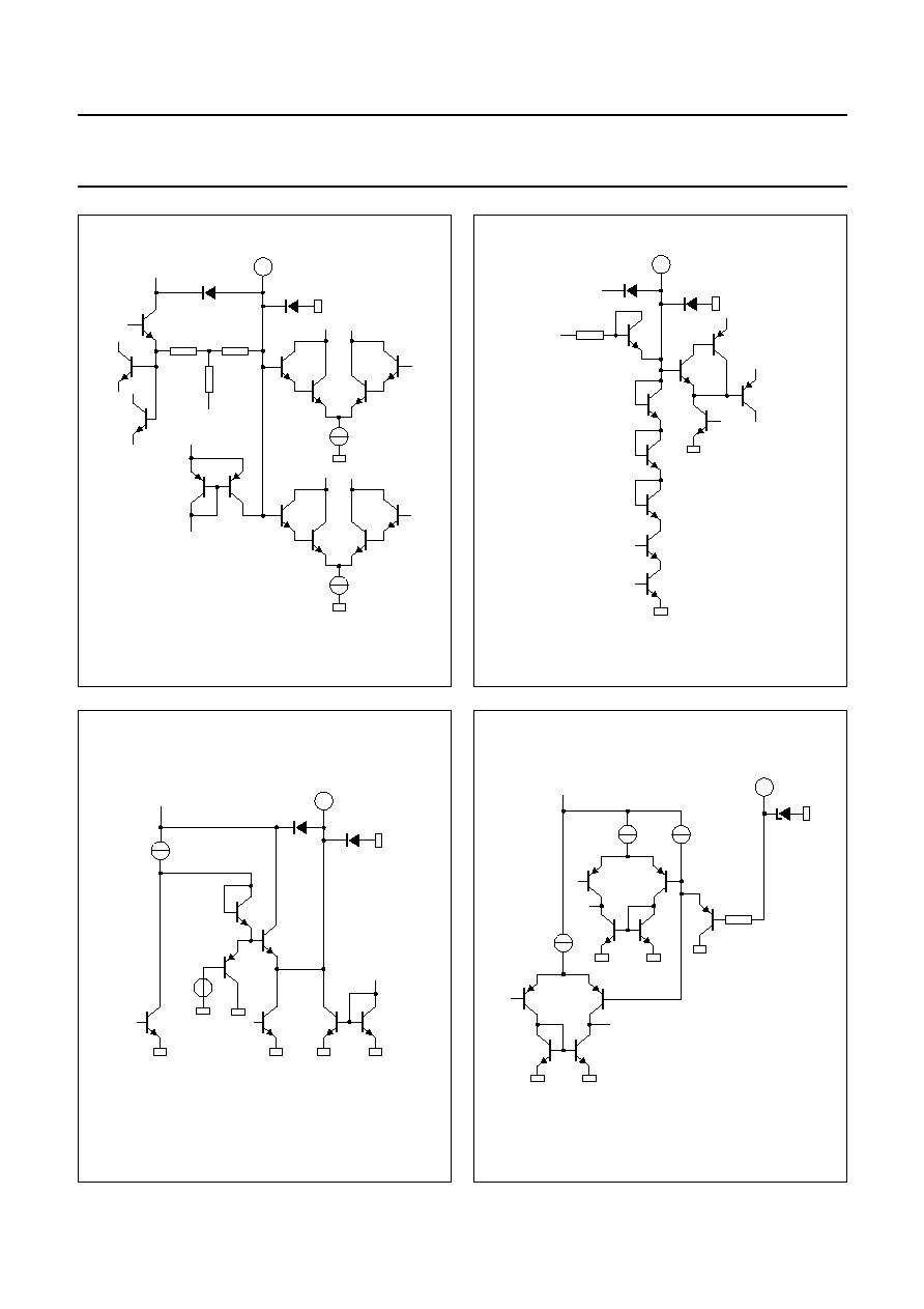
Fig.28 Pin 13: supply voltage.
handbook, halfpage
MHB143
13
10 V
Fig.29 Pins 14, 16, 17 and 19: input channel.
handbook, halfpage
MHB144
6.25
pF
5 V
240
100 k
+
14
5 V
Fig.30 Pin 15: reference voltage.
handbook, halfpage
MHB145
2.55 k
2.55 k
+
15
5 V
Fig.31 Pin 18: head switch input.
handbook, halfpage
MHB146
+
18
1998 Nov 12
29
Philips Semiconductors
Product specification
I
2
C-bus controlled dual Dolby* B-type noise
reduction circuit for playback applications
TEA0679T
Fig.32 Pin 25: control voltage channel B.
handbook, halfpage
MHB147
25
+
+
5 V
1.2 k
3.4 k
3.6 k
Fig.33 Pin 26: integrating filter channel B.
handbook, halfpage
MHB148
26
+
Vref
±
0.23 V
3.6 k
Fig.34 Pin 28: AMS output.
handbook, halfpage
28
+
MHB149
3 V
Fig.35 Pin 30: serial clock input.
handbook, halfpage
MHB150
+
1.9 k
30
1998 Nov 12
30
Philips Semiconductors
Product specification
I
2
C-bus controlled dual Dolby* B-type noise
reduction circuit for playback applications
TEA0679T
Fig.36 Pin 31: serial data input/output.
handbook, halfpage
MHB151
+
1.9 k
31
Fig.37 Pin 32: bus enable.
handbook, halfpage
MHB152
32
+
1998
Nov
12
31
Philips Semiconductors
Product specification
I
2
C-bus controlled dual Dolby* B-type noise
reduction circuit for playback applications
TEA0679T
This text is here in white to force landscape pages to be rotated correctly when browsing through the pdf in the Acrobat reader.This text is here in
_
white to force landscape pages to be rotated correctly when browsing through the pdf in the Acrobat reader.This text is here inThis text is here in
white to force landscape pages to be rotated correctly when browsing through the pdf in the Acrobat reader. white to force landscape pages to be ...
TEST AND APPLICA
TION INFORMA
TION
handbook, full pagewidth
MHB153
I
2
C-BUS
PRE
AMP
LOGIC
EQ
AMP
13
VCC = 10 V
PRE
AMP
EQ
AMP
POWER
SUPPLY
LEVEL
DETECTOR
DELAY
TIME
LATCH
AND
RISE TIME
AMS
PROCESSOR
MUTE
14
INA1
15
Vref
12
EQFA
11
EQA
16
INA2
DOLBY B
DOLBY B
20
AGND
BLANK
SKIP
19
INB1
18
HS
HS
(opt)
21
EQFB
22
EQB
17
INB2
TEA0679T
10
SCA
HPA
23
SCB
9
CONTRA
24
HPB
8
INTA
25
26
CONTRB
7
OUTA
27
INTB
6
5
EQS
EQS
(opt)
28
29
30
OUTB
DGND AMS
3
TD
SCL
2
BSC
31
SDA
1
MAD
32
BEN
4
BTC
output A
4.7 nF
15 nF
24 k
Rt
(ref)
180 k
10
µ
F
10 k
270 k
100 nF
47 nF
220 nF
330 nF
10
µ
F
output B
4.7 nF
15 nF
24 k
20 k
180 k
270 k
100 nF
330 nF
10
µ
F
10
µ
F
10 k
100
µ
F
100
nF
0.25 V (RMS)
1 kHz
1000
µ
F
20 k
10 k
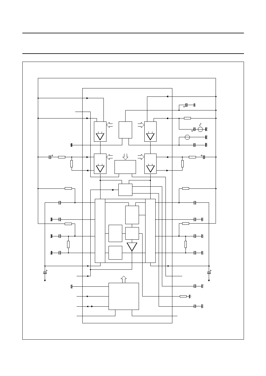
Fig.38 Test circuit for power supply ripple rejection.
1998
Nov
12
32
Philips Semiconductors
Product specification
I
2
C-bus controlled dual Dolby* B-type noise
reduction circuit for playback applications
TEA0679T
This text is here in white to force landscape pages to be rotated correctly when browsing through the pdf in the Acrobat reader.This text is here in
_
white to force landscape pages to be rotated correctly when browsing through the pdf in the Acrobat reader.This text is here inThis text is here in
white to force landscape pages to be rotated correctly when browsing through the pdf in the Acrobat reader. white to force landscape pages to be ...
a
ndbook, full pagewidth
MHB154
I
2
C-BUS
PRE
AMP
LOGIC
EQ
AMP
13
VCC
PRE
AMP
EQ
AMP
POWER
SUPPLY
LEVEL
DETECTOR
DELAY
TIME
LATCH
AND
RISE TIME
AMS
PROCESSOR
MUTE
14
INA1
15
Vref
12
EQFA
11
EQA
16
INA2
DOLBY B
DOLBY B
20
AGND
BLANK
SKIP
19
INB1
18
HS
HS
(opt)
21
EQFB
22
EQB
17
INB2
TEA0679T
10
SCA
HPA
23
SCB
9
CONTRA
24
HPB
8
INTA
25
26
CONTRB
7
OUTA
27
INTB
6
5
EQS
EQS
(opt)
28
29
30
OUTB
DGND AMS
3
TD
SCL
2
BSC
31
SDA
1
MAD
32
BEN
4
BTC
output A
4.7 nF
15 nF
24 k
Rt
(ref)
180 k
10
µ
F
10 k
270 k
100 nF
47 nF
220 nF
330 nF
10
µ
F
output B
4.7 nF
15 nF
24 k
20 k
180 k
270 k
100 nF
330 nF
10
µ
F
10
µ
F
10 k
200
100
µ
F
100
nF
20 k
10 V
10
µ
F
Fig.39 Test circuit for channel separation.
1998
Nov
12
33
Philips Semiconductors
Product specification
I
2
C-bus controlled dual Dolby* B-type noise
reduction circuit for playback applications
TEA0679T
This text is here in white to force landscape pages to be rotated correctly when browsing through the pdf in the Acrobat reader.This text is here in
_
white to force landscape pages to be rotated correctly when browsing through the pdf in the Acrobat reader.This text is here inThis text is here in
white to force landscape pages to be rotated correctly when browsing through the pdf in the Acrobat reader. white to force landscape pages to be ...
a
ndbook, full pagewidth
MHB155
I
2
C-BUS
PRE
AMP
LOGIC
EQ
AMP
13
VCC
PRE
AMP
EQ
AMP
POWER
SUPPLY
LEVEL
DETECTOR
DELAY
TIME
LATCH
AND
RISE TIME
AMS
PROCESSOR
MUTE
14
INA1
15
Vref
12
EQFA
11
EQA
16
INA2
DOLBY B
DOLBY B
20
AGND
BLANK
SKIP
19
INB1
18
HS
HS
(opt)
21
EQFB
22
EQB
17
INB2
TEA0679T
10
SCA
HPA
23
SCB
9
CONTRA
24
HPB
8
INTA
25
26
CONTRB
7
OUTA
27
INTB
6
5
EQS
EQS
(opt)
28
29
30
OUTB
DGND AMS
3
TD
SCL
2
BSC
31
SDA
1
MAD
32
BEN
4
BTC
output A
4.7 nF
15 nF
24 k
Rt
(ref)
180 k
10
µ
F
10 k
270 k
100 nF
47 nF
220 nF
330 nF
10
µ
F
output B
4.7 nF
15 nF
24 k
20 k
180 k
270 k
100 nF
330 nF
10
µ
F
10
µ
F
10 k
100
µ
F
100
nF
20 k
10 V
voltage
input
Fig.40 Test circuit for AMS threshold level.

1998
Nov
12
34
Philips Semiconductors
Product specification
I
2
C-bus controlled dual Dolby* B-type noise
reduction circuit for playback applications
TEA0679T
This text is here in white to force landscape pages to be rotated correctly when browsing through the pdf in the Acrobat reader.This text is here in
_
white to force landscape pages to be rotated correctly when browsing through the pdf in the Acrobat reader.This text is here inThis text is here in
white to force landscape pages to be rotated correctly when browsing through the pdf in the Acrobat reader. white to force landscape pages to be ...
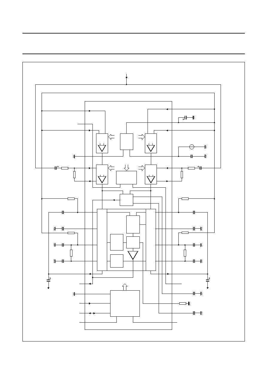
d
book, full pagewidth
MHB156
I
2
C-BUS
PRE
AMP
LOGIC
EQ
AMP
13
VCC
PRE
AMP
EQ
AMP
POWER
SUPPLY
LEVEL
DETECTOR
DELAY
TIME
LATCH
AND
RISE TIME
AMS
PROCESSOR
MUTE
14
INA1
15
Vref
12
EQFA
11
EQA
16
INA2
DOLBY B
DOLBY B
20
AGND
BLANK
SKIP
19
INB1
18
HS
HS
(opt)
21
EQFB
22
EQB
17
INB2
TEA0679T
10
SCA
HPA
23
SCB
9
CONTRA
24
HPB
8
INTA
25
26
CONTRB
7
OUTA
27
INTB
6
5
EQS
EQS
(opt)
28
29
30
OUTB
DGND AMS
3
TD
SCL
2
BSC
31
SDA
1
MAD
32
BEN
4
BTC
output A
4.7 nF
15 nF
24 k
Rt
(ref)
180 k
10
µ
F
10
µ
F
200
10 k
270 k
100 nF
47 nF
220 nF
330 nF
10
µ
F
output B
4.7 nF
15 nF
24 k
20 k
25 k
180 k
270 k
100 nF
330 nF
10
µ
F
10
µ
F
10 k
100
µ
F
100
nF
20 k
25 k
25 k
25 k
10 V
Vi
TP
TP
470
pF
10
µ
F
VCC
Vi
Fig.41 Test circuit for frequency response (channel B).
Channel A: Decode mode: pre-amplifier 30 dB and EQ amplifier 10 dB linear.
Channel B: Encode mode.

1998
Nov
12
35
Philips Semiconductors
Product specification
I
2
C-bus controlled dual Dolby* B-type noise
reduction circuit for playback applications
TEA0679T
This text is here in white to force landscape pages to be rotated correctly when browsing through the pdf in the Acrobat reader.This text is here in
_
white to force landscape pages to be rotated correctly when browsing through the pdf in the Acrobat reader.This text is here inThis text is here in
white to force landscape pages to be rotated correctly when browsing through the pdf in the Acrobat reader. white to force landscape pages to be ...
a
ndbook, full pagewidth
MHB157
200
470
pF
200
470
pF
200
470
pF
200
470
pF
I
2
C-BUS
PRE
AMP
LOGIC
EQ
AMP
13
VCC
PRE
AMP
EQ
AMP
POWER
SUPPLY
LEVEL
DETECTOR
DELAY
TIME
LATCH
AND
RISE TIME
AMS
PROCESSOR
MUTE
14
INA1
15
Vref
12
EQFA
11
EQA
16
INA2
DOLBY B
DOLBY B
20
AGND
BLANK
SKIP
19
INB1
18
HS
HS
(opt)
21
EQFB
22
EQB
17
INB2
TEA0679T
10
SCA
HPA
23
SCB
9
CONTRA
24
HPB
8
INTA
25
26
CONTRB
7
OUTA
27
INTB
6
5
EQS
EQS
(opt)
28
29
30
OUTB
DGND AMS
3
TD
SCL
2
BSC
31
SDA
1
MAD
32
BEN
4
BTC
output A
4.7 nF
15 nF
24 k
Rt
(ref)
180 k
10
µ
F
10 k
270 k
100 nF
47 nF
220 nF
330 nF
10
µ
F
output B
4.7 nF
15 nF
24 k
20 k
180 k
270 k
100 nF
330 nF
10
µ
F
10
µ
F
10 k
100
µ
F
100
nF
20 k
40
10
10 V
Fig.42 EMC test circuit.
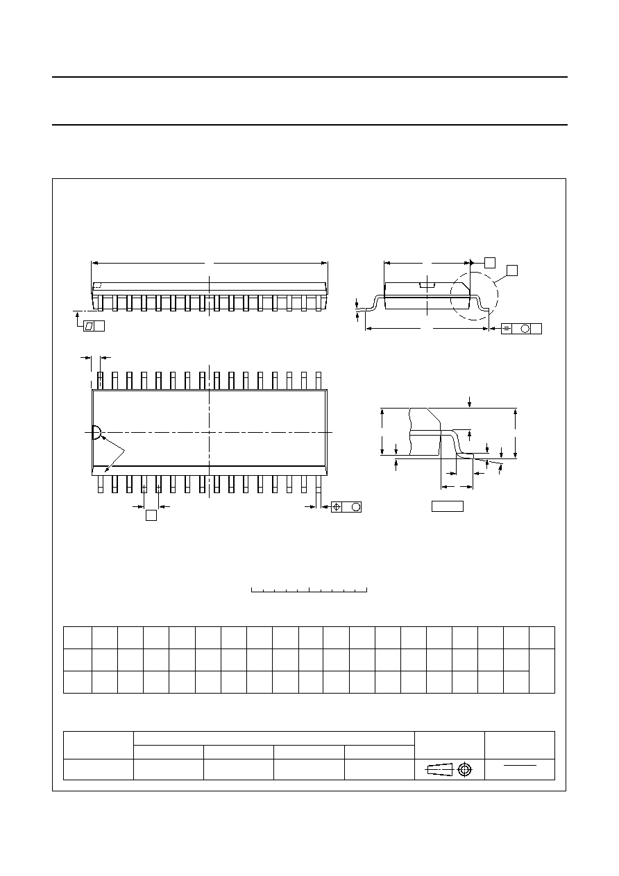
1998 Nov 12
36
Philips Semiconductors
Product specification
I
2
C-bus controlled dual Dolby* B-type noise
reduction circuit for playback applications
TEA0679T
PACKAGE OUTLINE
UNIT
A
max.
A
1
A
2
A
3
b
p
c
D
(1)
E
(1)
e
H
E
L
L
p
Q
Z
y
w
v
REFERENCES
OUTLINE
VERSION
EUROPEAN
PROJECTION
ISSUE DATE
IEC
JEDEC
EIAJ
mm
inches
2.65
0.10
0.25
0.01
1.4
0.055
0.3
0.1
2.45
2.25
0.49
0.36
0.27
0.18
20.7
20.3
7.6
7.4
1.27
10.65
10.00
1.2
1.0
0.95
0.55
8
0
o
o
0.25
0.1
0.004
0.25
DIMENSIONS (inch dimensions are derived from the original mm dimensions)
Note
1. Plastic or metal protrusions of 0.15 mm maximum per side are not included.
1.1
0.4
SOT287-1
(1)
0.012
0.004
0.096
0.086
0.02
0.01
0.050
0.047
0.039
0.419
0.394
0.30
0.29
0.81
0.80
0.011
0.007
0.037
0.022
0.01
0.01
0.043
0.016
w
M
b
p
D
H
E
Z
e
c
v
M
A
X
A
y
32
17
16
1
A
A
1
A
2
L
p
Q
detail X
L
(A )
3
E
pin 1 index
0
5
10 mm
scale
SO32: plastic small outline package; 32 leads; body width 7.5 mm
SOT287-1
95-01-25
97-05-22

1998 Nov 12
37
Philips Semiconductors
Product specification
I
2
C-bus controlled dual Dolby* B-type noise
reduction circuit for playback applications
TEA0679T
SOLDERING
Introduction
There is no soldering method that is ideal for all IC
packages. Wave soldering is often preferred when
through-hole and surface mounted components are mixed
on one printed-circuit board. However, wave soldering is
not always suitable for surface mounted ICs, or for
printed-circuits with high population densities. In these
situations reflow soldering is often used.
This text gives a very brief insight to a complex technology.
A more in-depth account of soldering ICs can be found in
our
"Data Handbook IC26; Integrated Circuit Packages"
(order code 9398 652 90011).
Reflow soldering
Reflow soldering techniques are suitable for all SO
packages.
Reflow soldering requires solder paste (a suspension of
fine solder particles, flux and binding agent) to be applied
to the printed-circuit board by screen printing, stencilling or
pressure-syringe dispensing before package placement.
Several techniques exist for reflowing; for example,
thermal conduction by heated belt. Dwell times vary
between 50 and 300 seconds depending on heating
method. Typical reflow temperatures range from
215 to 250
∞
C.
Preheating is necessary to dry the paste and evaporate
the binding agent. Preheating duration: 45 minutes at
45
∞
C.
Wave soldering
Wave soldering techniques can be used for all SO
packages if the following conditions are observed:
∑
A double-wave (a turbulent wave with high upward
pressure followed by a smooth laminar wave) soldering
technique should be used.
∑
The longitudinal axis of the package footprint must be
parallel to the solder flow.
∑
The package footprint must incorporate solder thieves at
the downstream end.
During placement and before soldering, the package must
be fixed with a droplet of adhesive. The adhesive can be
applied by screen printing, pin transfer or syringe
dispensing. The package can be soldered after the
adhesive is cured.
Maximum permissible solder temperature is 260
∞
C, and
maximum duration of package immersion in solder is
10 seconds, if cooled to less than 150
∞
C within
6 seconds. Typical dwell time is 4 seconds at 250
∞
C.
A mildly-activated flux will eliminate the need for removal
of corrosive residues in most applications.
Repairing soldered joints
Fix the component by first soldering two diagonally-
opposite end leads. Use only a low voltage soldering iron
(less than 24 V) applied to the flat part of the lead. Contact
time must be limited to 10 seconds at up to 300
∞
C. When
using a dedicated tool, all other leads can be soldered in
one operation within 2 to 5 seconds between
270 and 320
∞
C.

1998 Nov 12
38
Philips Semiconductors
Product specification
I
2
C-bus controlled dual Dolby* B-type noise
reduction circuit for playback applications
TEA0679T
DEFINITIONS
LIFE SUPPORT APPLICATIONS
These products are not designed for use in life support appliances, devices, or systems where malfunction of these
products can reasonably be expected to result in personal injury. Philips customers using or selling these products for
use in such applications do so at their own risk and agree to fully indemnify Philips for any damages resulting from such
improper use or sale
PURCHASE OF PHILIPS I
2
C COMPONENTS
Data sheet status
Objective specification
This data sheet contains target or goal specifications for product development.
Preliminary specification
This data sheet contains preliminary data; supplementary data may be published later.
Product specification
This data sheet contains final product specifications.
Limiting values
Limiting values given are in accordance with the Absolute Maximum Rating System (IEC 134). Stress above one or
more of the limiting values may cause permanent damage to the device. These are stress ratings only and operation
of the device at these or at any other conditions above those given in the Characteristics sections of the specification
is not implied. Exposure to limiting values for extended periods may affect device reliability.
Application information
Where application information is given, it is advisory and does not form part of the specification.
Purchase of Philips I
2
C components conveys a license under the Philips' I
2
C patent to use the
components in the I
2
C system provided the system conforms to the I
2
C specification defined by
Philips. This specification can be ordered using the code 9398 393 40011.

1998 Nov 12
39
Philips Semiconductors
Product specification
I
2
C-bus controlled dual Dolby* B-type noise
reduction circuit for playback applications
TEA0679T
NOTES

Internet: http://www.semiconductors.philips.com
Philips Semiconductors ≠ a worldwide company
© Philips Electronics N.V. 1998
SCA60
All rights are reserved. Reproduction in whole or in part is prohibited without the prior written consent of the copyright owner.
The information presented in this document does not form part of any quotation or contract, is believed to be accurate and reliable and may be changed
without notice. No liability will be accepted by the publisher for any consequence of its use. Publication thereof does not convey nor imply any license
under patent- or other industrial or intellectual property rights.
Middle East: see Italy
Netherlands: Postbus 90050, 5600 PB EINDHOVEN, Bldg. VB,
Tel. +31 40 27 82785, Fax. +31 40 27 88399
New Zealand: 2 Wagener Place, C.P.O. Box 1041, AUCKLAND,
Tel. +64 9 849 4160, Fax. +64 9 849 7811
Norway: Box 1, Manglerud 0612, OSLO,
Tel. +47 22 74 8000, Fax. +47 22 74 8341
Pakistan: see Singapore
Philippines: Philips Semiconductors Philippines Inc.,
106 Valero St. Salcedo Village, P.O. Box 2108 MCC, MAKATI,
Metro MANILA, Tel. +63 2 816 6380, Fax. +63 2 817 3474
Poland: Ul. Lukiska 10, PL 04-123 WARSZAWA,
Tel. +48 22 612 2831, Fax. +48 22 612 2327
Portugal: see Spain
Romania: see Italy
Russia: Philips Russia, Ul. Usatcheva 35A, 119048 MOSCOW,
Tel. +7 095 755 6918, Fax. +7 095 755 6919
Singapore: Lorong 1, Toa Payoh, SINGAPORE 319762,
Tel. +65 350 2538, Fax. +65 251 6500
Slovakia: see Austria
Slovenia: see Italy
South Africa: S.A. PHILIPS Pty Ltd., 195-215 Main Road Martindale,
2092 JOHANNESBURG, P.O. Box 7430 Johannesburg 2000,
Tel. +27 11 470 5911, Fax. +27 11 470 5494
South America: Al. Vicente Pinzon, 173, 6th floor,
04547-130 S√O PAULO, SP, Brazil,
Tel. +55 11 821 2333, Fax. +55 11 821 2382
Spain: Balmes 22, 08007 BARCELONA,
Tel. +34 93 301 6312, Fax. +34 93 301 4107
Sweden: Kottbygatan 7, Akalla, S-16485 STOCKHOLM,
Tel. +46 8 5985 2000, Fax. +46 8 5985 2745
Switzerland: Allmendstrasse 140, CH-8027 ZÐRICH,
Tel. +41 1 488 2741 Fax. +41 1 488 3263
Taiwan: Philips Semiconductors, 6F, No. 96, Chien Kuo N. Rd., Sec. 1,
TAIPEI, Taiwan Tel. +886 2 2134 2865, Fax. +886 2 2134 2874
Thailand: PHILIPS ELECTRONICS (THAILAND) Ltd.,
209/2 Sanpavuth-Bangna Road Prakanong, BANGKOK 10260,
Tel. +66 2 745 4090, Fax. +66 2 398 0793
Turkey: Talatpasa Cad. No. 5, 80640 GÐLTEPE/ISTANBUL,
Tel. +90 212 279 2770, Fax. +90 212 282 6707
Ukraine: PHILIPS UKRAINE, 4 Patrice Lumumba str., Building B, Floor 7,
252042 KIEV, Tel. +380 44 264 2776, Fax. +380 44 268 0461
United Kingdom: Philips Semiconductors Ltd., 276 Bath Road, Hayes,
MIDDLESEX UB3 5BX, Tel. +44 181 730 5000, Fax. +44 181 754 8421
United States: 811 East Arques Avenue, SUNNYVALE, CA 94088-3409,
Tel. +1 800 234 7381
Uruguay: see South America
Vietnam: see Singapore
Yugoslavia: PHILIPS, Trg N. Pasica 5/v, 11000 BEOGRAD,
Tel. +381 11 625 344, Fax.+381 11 635 777
For all other countries apply to: Philips Semiconductors,
International Marketing & Sales Communications, Building BE-p, P.O. Box 218,
5600 MD EINDHOVEN, The Netherlands, Fax. +31 40 27 24825
Argentina: see South America
Australia: 34 Waterloo Road, NORTH RYDE, NSW 2113,
Tel. +61 2 9805 4455, Fax. +61 2 9805 4466
Austria: Computerstr. 6, A-1101 WIEN, P.O. Box 213, Tel. +43 160 1010,
Fax. +43 160 101 1210
Belarus: Hotel Minsk Business Center, Bld. 3, r. 1211, Volodarski Str. 6,
220050 MINSK, Tel. +375 172 200 733, Fax. +375 172 200 773
Belgium: see The Netherlands
Brazil: see South America
Bulgaria: Philips Bulgaria Ltd., Energoproject, 15th floor,
51 James Bourchier Blvd., 1407 SOFIA,
Tel. +359 2 689 211, Fax. +359 2 689 102
Canada: PHILIPS SEMICONDUCTORS/COMPONENTS,
Tel. +1 800 234 7381
China/Hong Kong: 501 Hong Kong Industrial Technology Centre,
72 Tat Chee Avenue, Kowloon Tong, HONG KONG,
Tel. +852 2319 7888, Fax. +852 2319 7700
Colombia: see South America
Czech Republic: see Austria
Denmark: Prags Boulevard 80, PB 1919, DK-2300 COPENHAGEN S,
Tel. +45 32 88 2636, Fax. +45 31 57 0044
Finland: Sinikalliontie 3, FIN-02630 ESPOO,
Tel. +358 9 615800, Fax. +358 9 61580920
France: 51 Rue Carnot, BP317, 92156 SURESNES Cedex,
Tel. +33 1 40 99 6161, Fax. +33 1 40 99 6427
Germany: Hammerbrookstraþe 69, D-20097 HAMBURG,
Tel. +49 40 23 53 60, Fax. +49 40 23 536 300
Greece: No. 15, 25th March Street, GR 17778 TAVROS/ATHENS,
Tel. +30 1 4894 339/239, Fax. +30 1 4814 240
Hungary: see Austria
India: Philips INDIA Ltd, Band Box Building, 2nd floor,
254-D, Dr. Annie Besant Road, Worli, MUMBAI 400 025,
Tel. +91 22 493 8541, Fax. +91 22 493 0966
Indonesia: PT Philips Development Corporation, Semiconductors Division,
Gedung Philips, Jl. Buncit Raya Kav.99-100, JAKARTA 12510,
Tel. +62 21 794 0040 ext. 2501, Fax. +62 21 794 0080
Ireland: Newstead, Clonskeagh, DUBLIN 14,
Tel. +353 1 7640 000, Fax. +353 1 7640 200
Israel: RAPAC Electronics, 7 Kehilat Saloniki St, PO Box 18053,
TEL AVIV 61180, Tel. +972 3 645 0444, Fax. +972 3 649 1007
Italy: PHILIPS SEMICONDUCTORS, Piazza IV Novembre 3,
20124 MILANO, Tel. +39 2 6752 2531, Fax. +39 2 6752 2557
Japan: Philips Bldg 13-37, Kohnan 2-chome, Minato-ku,
TOKYO 108-8507, Tel. +81 3 3740 5130, Fax. +81 3 3740 5077
Korea: Philips House, 260-199 Itaewon-dong, Yongsan-ku, SEOUL,
Tel. +82 2 709 1412, Fax. +82 2 709 1415
Malaysia: No. 76 Jalan Universiti, 46200 PETALING JAYA, SELANGOR,
Tel. +60 3 750 5214, Fax. +60 3 757 4880
Mexico: 5900 Gateway East, Suite 200, EL PASO, TEXAS 79905,
Tel. +9-5 800 234 7381
Printed in The Netherlands
545102/750/02/pp40
Date of release: 1998 Nov 12
Document order number:
9397 750 04298