Document Outline
- GENERAL DESCRIPTION
- FEATURES
- PACKAGE OUTLINES
- Block diagram
- QUICK REFERENCE DATA
- PINNING
- FUNCTIONAL DESCRIPTION
- Supplies VCC1 , VCC2 , LN, SLPE, REG and STAB
- Microphone inputs MIC+ and MIC- and gain pins GAS1 and GAS2
- Dynamic limiter (microphone) pin DLS/MMUTE
- Receiving amplifier IR, QR+, QR- and GAR
- Automatic gain control input AGC
- MUTE input
- Dual-tone multi-frequency input DTMF
- Power-down input PD
- Side-tone suppression
- RATINGS
- THERMAL RESISTANCE
- CHARACTERISTICS
- APPLICATION INFORMATION
- PACKAGE OUTLINES
- SOLDERING
- DEFINITIONS
- LIFE SUPPORT APPLICATIONS

DATA SHEET
Product specification
File under Integrated Circuits, IC03A
March 1994
INTEGRATED CIRCUITS
TEA1064A
Low voltage versatile telephone
transmission circuit with dialler
interface and transmit level
dynamic limiting

March 1994
2
Philips Semiconductors
Product specification
Low voltage versatile telephone transmission circuit
with dialler interface and transmit level dynamic limiting
TEA1064A
GENERAL DESCRIPTION
The TEA1064A is a bipolar integrated circuit that performs
all the speech and line interface functions required in fully
electronic telephone sets. It performs electronic switching
between dialling and speech and has a powerful DC
supply for peripheral circuits. The IC operates at line
voltages down to 1.8 V DC (with reduced performance) to
facilitate the use of more telephone sets connected in
parallel. The transmit signal on the line is dynamically
limited (speech-controlled) to prevent distortion at high
transmit levels of both the sending signal and the sidetone.
FEATURES
∑
Low DC line voltage; operates down to 1.8 V (excluding
polarity guard)
∑
Voltage regulator with low voltage drop and adjustable
static resistance
∑
DC line voltage adjustment facility
∑
Provides a supply for external circuits in two options:
unregulated supply, regulated line voltage;
stabilized supply, line voltage varies with supply
current
∑
Dynamic limiting (speech-controlled) in transmit
direction prevents distortion of line signal and sidetone
∑
Symmetrical high-impedance inputs (64 k
) for
dynamic, magnetic or piezo-electric microphones
∑
Asymmetrical high-impedance input (32 k
) for electret
microphones
∑
DTMF signal input
∑
Confidence tone in the earpiece during DTMF dialling
∑
Mute input for disabling speech during pulse or DTMF
dialling
∑
Power-down input for improved performance during
pulse dial or register recall (flash)
∑
Receiving amplifier for magnetic, dynamic or
piezo-electric earpieces
∑
Large amplification setting ranges on microphone and
earpiece amplifiers
∑
Line loss compensation (line current dependent) for
microphone and earpiece amplifiers (not used for DTMF
amplifier)
∑
Gain control curve adaptable to exchange supply
∑
Automatic disabling of the DTMF amplifier in
extremely-low voltage conditions
∑
Microphone MUTE function available with switch
PACKAGE OUTLINES
Notes
1. SOT146-1; 1998 Jun 18.
2. SOT163-1; 1998 Jun 18.
TEA1064A :20-lead DIL; plastic (SOT146).
(1)
TEA1064AT:20-lead mini-pack; plastic (SO20;
SOT163A).
(2)

March 1994
3
Philips Semiconductors
Product specification
Low voltage versatile telephone transmission circuit
with dialler interface and transmit level dynamic limiting
TEA1064A
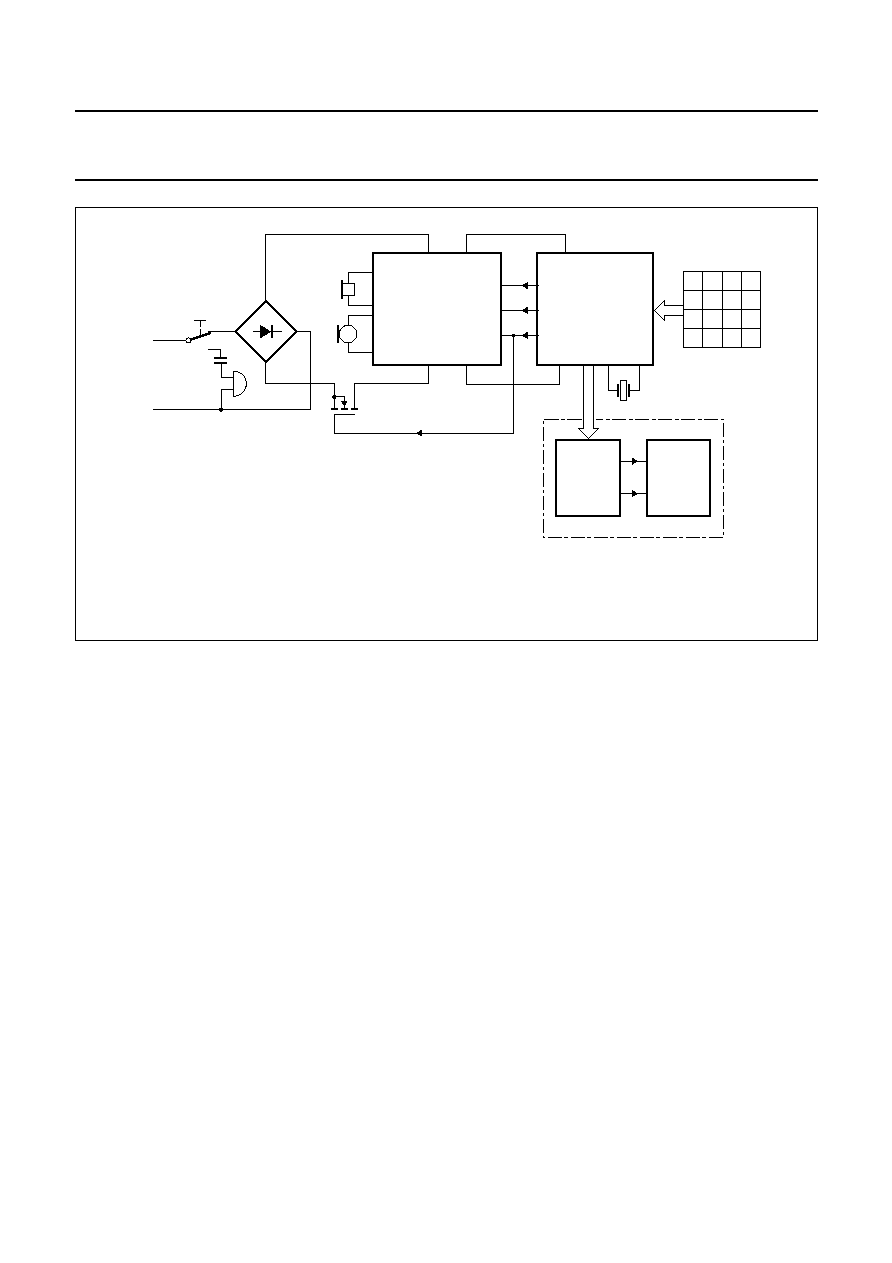
Fig.1 Block diagram.
handbook, full pagewidth
+
MGR056
CURRENT
REFERENCE
START
CIRCUIT
DYNAMIC
LIMITER
LOW
VOLTAGE
CIRCUIT
AGC
CIRCUIT
SUPPLY AND
REFERENCE
17
11
VEE
REG
AGC
STAB
DLS/MMUTE
SLPE
GAS2
GAS1
QR
-
QR
+
GAR
LN
VCC1
15
14
12
dB
8
9
+
-
+
-
18
10
7
20
13
IR
MIC
+
MIC
-
DTMF
MUTE
PD
+
-
+
-
-
1
16
TEA1064A
6
5
4
2
VCC2
19
3
March 1994
4
Philips Semiconductors
Product specification
Low voltage versatile telephone transmission circuit
with dialler interface and transmit level dynamic limiting
TEA1064A
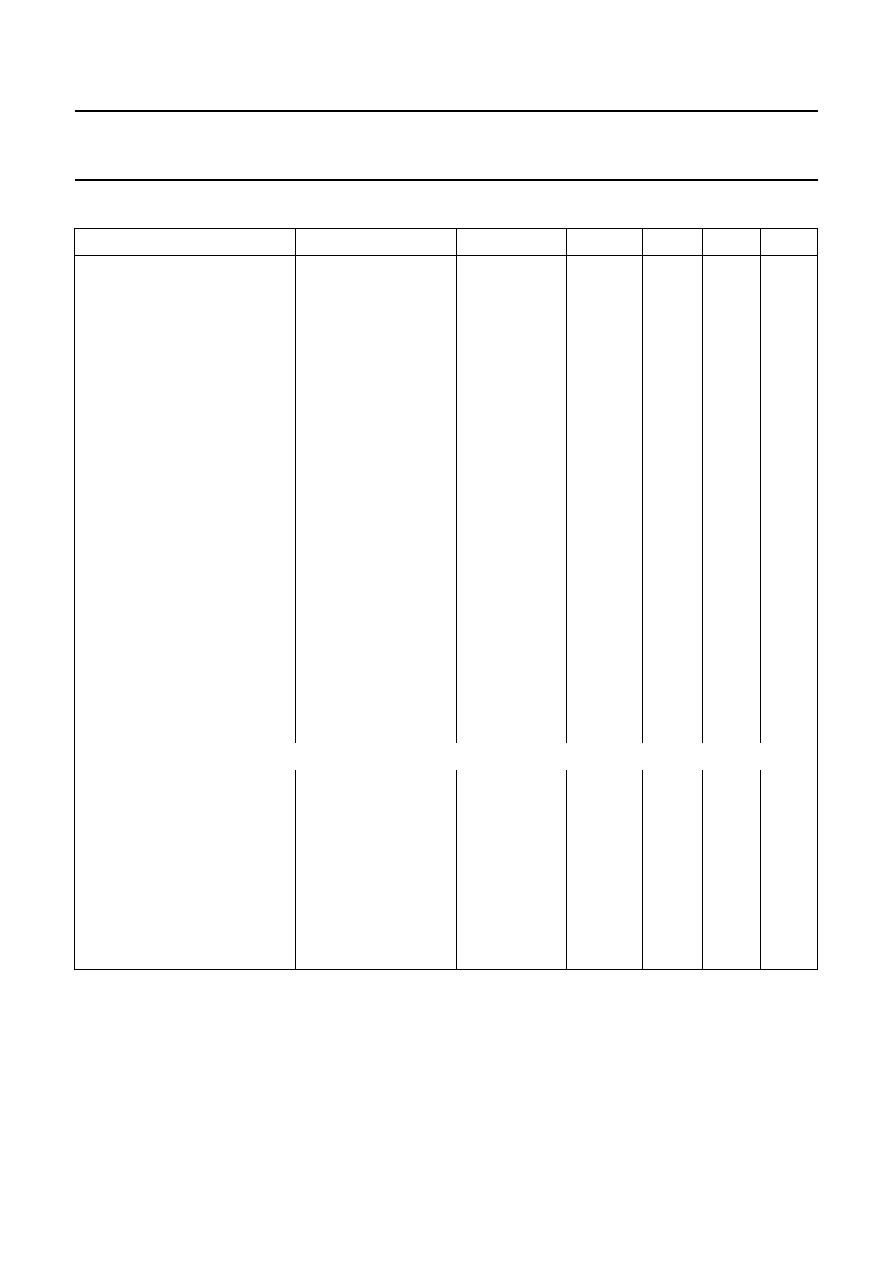
QUICK REFERENCE DATA
PARAMETER
CONDITIONS
SYMBOL
MIN.
TYP.
MAX.
UNIT
Operating ambient temperature
range
T
amb
-
25
-
+
75
∞
C
Line current operating range:
normal operation
l
line
11
-
140
(1)
mA
with reduced performance
l
line
2
-
11
mA
Internal supply current:
power-down input LOW
V
CC1
= 2.8 V
I
CC1
-
1.3
1.6
mA
power-down input HIGH
V
CC1
= 2.8 V
I
CC1
-
60
82
µ
A
Voltage gain range:
microphone amplifier
G
v
44
-
52
dB
receiving amplifier
G
v
20
-
45
dB
Line loss compensation:
gain control range
G
v
5.7
6.1
6.5
dB
exchange supply voltage
range
V
exch
36
-
60
V
exchange feeding bridge
resistance range
R
exch
400
-
1000
Maximum output voltage swing
on LN (peak-to-peak value)
R15
+
R16 = 448
l
line
= 15 mA
I
p
= 2 mA
V
LN(p-p)
3.7
3.95
4.2
V
I
p
= 4 mA
V
LN(p-p)
3.0
3.25
3.5
V
Regulated line voltage application
R15 = 0
;
R16 = 392
Supply for peripherals
l
line
= 15 mA
I
p
= 1.4 mA
V
p
2.5
-
-
V
I
p
= 2.7 mA;
R
REG-SLPE
= 20 k
V
p
2.9
-
-
V
DC line voltage
l
line
= 15 mA
without R
REG-SLPE
V
LN
-
3.57
-
V
R
REG-SLPE
= 20 k
V
LN
-
4.57
-
V
March 1994
5
Philips Semiconductors
Product specification
Low voltage versatile telephone transmission circuit
with dialler interface and transmit level dynamic limiting
TEA1064A
Note
1. For TEA1064AT the maximum line current depends on the heat dissipating qualities of the mounted device.
Stabilized supply voltage application
R15 = 392
;
R16 = 56
Supply for peripherals
l
line
= 15 mA
I
p
= 0 to 4 mA
V
CC2-SLPE
3.05
3.3
3.55
V
DC line voltage
l
line
= 15 mA
I
p
= 2 mA
V
LN
4.2
4.4
4.8
V
I
p
= 4 mA
V
LN
4.9
5.1
5.5
V
PARAMETER
CONDITIONS
SYMBOL
MIN.
TYP.
MAX.
UNIT
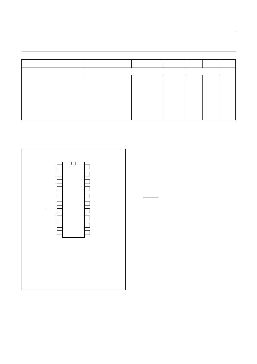
PINNING
Fig.2 Pinning diagram.
handbook, halfpage
LN
GAS1
GAS2
QR
-
QR
+
GAR
DLS/MMUTE
MIC
-
MIC
+
STAB
SLPE
VCC2
AGC
REG
PD
MUTE
VCC1
IR
DTMF
VEE
1
2
3
4
5
6
7
8
9
10
11
12
20
19
18
17
16
15
14
13
TEA1064A
MGR057
1 LN
positive line terminal
2 GAS1
gain adjustment; transmitting amplifier
3 GAS2
gain adjustment; transmitting amplifier
4 QR
-
inverting output, receiving amplifier
5 QR
+
non-inverting output, receiving
amplifier
6 GAR
gain adjustment; receiving amplifier
7 DLS/
MMUTE
decoupling for transmit amplifier
dynamic and microphone MUTE input
8 MIC
-
inverting microphone input
9 MIC
+
non-inverting microphone input
10 STAB
current stabilizer
11 V
EE
negative line terminal
12 DTMF
dual-tone multi-frequency input
13 IR
receiving amplifier input
14 MUTE
mute input
15 PD
power-down input
16 V
CC1
internal supply decoupling
17 REG
voltage regulator decoupling
18 AGC
automatic gain control input
19 V
CC2
reference voltage with respect to SLPE
20 SLPE
slope adjustment for DC
curve/reference for peripheral circuits.

March 1994
6
Philips Semiconductors
Product specification
Low voltage versatile telephone transmission circuit
with dialler interface and transmit level dynamic limiting
TEA1064A
FUNCTIONAL DESCRIPTION
Supplies V
CC1
, V
CC2
, LN, SLPE, REG and STAB (Fig.3)
Power for the TEA1064A and its peripheral circuits is
usually obtained from the telephone line. The IC develops
its own supply voltage at V
CC1
and regulates its voltage
drop. The internal supply requires a decoupling capacitor
between V
CC1
and V
EE
. The internal current stabilizer is
set by a 3.6 k
resistor between STAB and V
EE
.
The DC current flowing into the set is determined by the
exchange supply voltage V
exch
, the feeding bridge
resistance R
exch
, the subscriber line DC resistance R
line
and the DC voltage (including polarity guard) on the
subscriber set (see Fig.3).
The internal voltage regulator generates a
temperature-compensated reference voltage that is
available between V
CC2
and SLPE
[V
ref
= V
CC2-SLPE
= 3.3 V (typ.)]. This internal voltage
regulator requires decoupling by a capacitor between REG
and V
EE
(C3).
The reference voltage can be used to:
∑
regulate directly the line voltage (stabilized
V
LN-SLPE
= V
CC2-SLPE
)
(1)
∑
to stabilize the supply voltage for peripherals.
Regulated line voltage
In this application the V
CC2
pin is connected to the LN pin
as shown in Fig.3. This configuration gives a stabilized
voltage across pins LN and SLPE which, applied via the
low-pass filter R16, C15, provides a supply to the
peripherals that is independent of the line current and
depends only on the peripheral supply current.
The value of R16 and the level of the DC voltage V
LN-SLPE
determine the supply capabilities. In the basic application
R16 = 392
and C15 = 220
µ
F. The worst-case
peripheral supply current as a function of supply voltage is
shown in Fig.4. To increase the supply capabilities, the DC
voltage V
LN-SLPE
can be increased by using R
VA(REG-SLPE)
or by decreasing the value of R16.
(1) The TEA1064A application with regulated line voltage is the
same as is used for TEA1060/TEA1061, TEA1067 and
TEA1068 integrated circuits.
Fig.3 Application with regulated line voltage (stabilized V
LN-SLPE
).
The voltage V
LN-SLPE
is fixed to V
ref
= 3.3
±
0.25 V. Resistor R16 together with the
line current determine the supply capabilities and the maximum output swing on
the line (no loop damping is necessary).
The line voltage V
LN
= V
ref
+
([I
line
-
1.55 mA]
◊
R9).
handbook, full pagewidth
MGR058
Rexch
Rline
Iline
Vexch
DC
AC
17
REG
C3
R5
R9
10
STAB
20
SLPE
LN
1
VCC1
16
19 VCC2
11
VEE
0.25 mA
R1
ISLPE
ICC1
R16
C1
C15
peripheral
circuits
Vp
Ip
TEA1064A
Ip
+
0.25 mA
March 1994
7
Philips Semiconductors
Product specification
Low voltage versatile telephone transmission circuit
with dialler interface and transmit level dynamic limiting
TEA1064A
The maximum AC output swing on the line at low line
currents is influenced by R16 (limited by current) and the
maximum output swing on the line at high line currents is
influenced by the DC voltage V
LN-SLPE
(limited by voltage).
In both these situations, the internal dynamic limiter in the
sending channel prevents distortion when the microphone
input is overdriven. The maximum AC output swing on LN
is shown in Fig.5; practical values for R16 are from 200 to
600
and this influences both the maximum output swing
at low line currents and the supply capabilities.
The SLPE pin is the ground reference for peripheral
circuits, therefore inputs MUTE, PD and DTMF are also
referenced to SLPE.
Active microphones can be supplied between V
CC1
and
V
EE
. Low-power circuits that provide only MUTE and/or PD
inputs to the TEA1064A also can be powered from V
CC1
.
However V
CC1
cannot be used for circuits that provide
DTMF signals to the TEA1064A because V
CC1
is referred
to ground.
If the line current l
line
exceeds I
CC1
+
0.25 mA, the voltage
converter shunts the excess current to SLPE via LN;
where I
CC1
1.3 mA, the value required by the IC for
normal operation.
Fig.4
Minimum supply current for peripherals (I
p
)
as a function of the peripheral supply
voltage (V
p
).
handbook, halfpage
2
5
0
1
MGR059
2
3
4
3
4
Vp (V)
Ip
(mA)
R
VA (REG-SLPE)
= 20 k
without
R
VA (REG-SLPE)
l
line
= 15 mA; R16 = 392
; R15 = 0
; valid for MUTE = 0 and 1.
Line current has very little influence
The DC line voltage on LN is:
V
LN
= V
LN-SLPE
+
(I
SLPE
◊
R9)
V
LN
= V
ref
+
([I
line
-
I
CC1
-
0.25
◊
10
-
3
A]
◊
R9)
in which
V
ref
= 3.3 V
±
0.25 V is the internal reference voltage
between V
CC2
and SLPE; its value can be adjusted by
external resistor R
VA
R9 = external resistor between SLPE and V
EE
(20
in
basic application).
With R9 = 20
, this results in:
V
LN
= 3.57
±
0.25 V at l
line
= 15 mA
V
LN
= 4.17
±
0.3 V at l
line
= 15 mA,
R
VA(REG-SLPE)
= 33 k
V
LN
= 4.57
±
0.35 V at l
line
= 15 mA,
R
VA(REG-SLPE)
= 20 k
The preferred value for R9 is 20
. Changing R9
influences microphone gain, DTMF gain, the gain control
characteristics, sidetone, and the DC characteristics
(especially the low voltage characteristics).
In normal conditions, I
SLPE
>> (I
CC1
+
0.25 mA) and the
static behaviour is equivalent to a voltage regulator diode
with an internal resistance of R9. In the audio frequency
range the dynamic impedance is determined mainly by R1.
The equivalent impedance of the circuit in the audio
frequency range is shown in Fig.6.
The internal reference voltage V
CC2-SLPE
can be increased
by external resistor R
VA(REG-SLPE)
connected between
REG and SLPE. The supply voltage V
CC2-SLPE
is shown as
a function of R
VA(REG-SLPE)
in Fig.7. Changing the
reference voltage influences the output swing of both
sending and receiving amplifiers.
At line currents below 8 mA (typ.), the DC voltage dropped
across the circuit is adjusted to a lower level automatically
(approximately 1.8 V at 2 mA). This gives the possibility of
operating more telephone sets in parallel with DC line
voltages (excluding polarity guard) down to an absolute
minimum of 1.8 V. At line currents below 8 mA (typ.), the
circuit has limited sending and receiving levels.
March 1994
8
Philips Semiconductors
Product specification
Low voltage versatile telephone transmission circuit
with dialler interface and transmit level dynamic limiting
TEA1064A
Fig.5
Maximum AC output swing on the line as a
function of line current with peripheral
supply current as a parameter: R15 = 0
;
R16 = 392
.
handbook, halfpage
10
6
4
2
0
20
30
MGR060
Iline (mA)
VLN(p-p)
(V)
Ip =
0 mA
2 mA
4 mA
Fig.6
Equivalent impedance between LN and
V
EE
in the application with stabilized
V
LN-SLPE
:
R15 = 0
L
eq
= C3
◊
R9
◊
R
p
R
p
= 15 k
handbook, halfpage
MGR061
R9
20
REG
LN
C3
4.7
µ
F
Rp
Vref
Leq
VCC1
VEE
C1
R1
Fig.7
Internal reference voltage V
CC2-SLPE
as a function of resistor R
VA(REG-SLPE)
for line currents between 11
and 140 mA.
In the stabilized supply application:
V
LN
= V
CC2-SLPE
+
([I
p
+
0.25
◊
10
-
3
A]
◊
R15)
+
([I
line
-
1.55
◊
10
-
3
A]
◊
R9)
In the unregulated supply application (R15 = 0
):
V
LN
= V
CC2-SLPE
+
([I
line
-
1.55
◊
10
-
3
A]
◊
R9)
handbook, full pagewidth
7.8
3.0
0
80
40
120
MGR062
4.2
5.4
6.6
RVA (REG-SLPE) (k
)
Vref
(V)
with RVA
infinite

March 1994
9
Philips Semiconductors
Product specification
Low voltage versatile telephone transmission circuit
with dialler interface and transmit level dynamic limiting
TEA1064A
Stabilized peripheral supply voltage
The configuration shown in Fig.8 provides a stabilized
voltage across pins V
CC2
and SLPE for peripheral circuits
(such as dialling and control circuits); the DC voltage
V
LN
now varies with the peripheral supply current.
The V
CC2-SLPE
supply must be decoupled by capacitor
C15. For stable loop operation, resistor R16 (
50
) is
connected between V
CC2
and SLPE in series with C15.
The voltage regulator control loop is completed by resistor
R15 between LN and V
CC2
.
For sets with an impedance of 600
, practical values are:
R15 = 200 to 600
; C15 = 220
µ
F; C3 = 470 nF. The
ratio R15/R16
8 is for stable loop operation with
sufficient phase margin, and R15/R16
6 is for
satisfactory set impedance in the audio frequency range.
For sets with complex impedance, the value of C3 and the
ratio R15/R16 are different (further information is given in
the TEA1064A Application Report
(1)
).
The peripheral supply capability depends mainly on the
available line current, the required AC output swing on the
line, the maximum permitted DC voltage on the line and
the values of external components (especially R15). With
R15 = 392
and R16 = 56
(basic application) the
maximum possible AC output swing on the line as a
function of line current is as shown in Fig.9, the curve
parameter is the peripheral supply current (I
p
). Different
values for R15 (from 200 to 600
) maintaining
6
<
R15/R16
<
8 give different results (these are described
in the TEA1064A Application Report
(1)
.
(1) Supplied on request.
Fig.8 Application with stabilized supply voltage for peripheral circuits: R15 = 392
; R16 = 56
.
handbook, full pagewidth
MGR063
Rexch
Rline
Iline
Vexch
DC
AC
17
REG
C3
R5
R9
10
STAB
20
SLPE
LN
1
VCC1
16
19 VCC2
11
VEE
0.25 mA
R1
R15
ISLPE
ICC1
R16
C1
C15
peripheral
circuits
Vp
Ip
TEA1064A
Ip
+
0.25 mA
March 1994
10
Philips Semiconductors
Product specification
Low voltage versatile telephone transmission circuit
with dialler interface and transmit level dynamic limiting
TEA1064A
The DC line voltage on LN is
V
LN
= V
LN-SLPE
+
(I
SLPE
◊
R9).
Therefore
V
LN
= V
ref
+
([I
p
+
0.25
◊
10
-
3
A]
◊
R15)
+
([l
line
-
I
CC1
-
0.25
◊
10
-
3
A]
◊
R9)
in which:
V
ref
is the internal reference voltage between V
CC2
and
SLPE (the value of V
ref
can be adjusted by an external
resistor, R
VA
). V
ref
= 3.3 V (typ.) without R
VA
I
p
is the supply current used by peripheral circuits
R15 is an external resistor between LN and V
CC2
(392
in the basic application)
R9 is an external resistor between SLPE and
V
EE
(20
in the basic application)
The DC voltage V
LN-SLPE
as a function of I
p
with R15 as a
parameter is shown in Fig.10. In the audio frequency
range, the dynamic impedance is determined mainly by
R1. The equivalent impedance in the audio range of the
circuit (Fig.8) is shown in Fig.11.
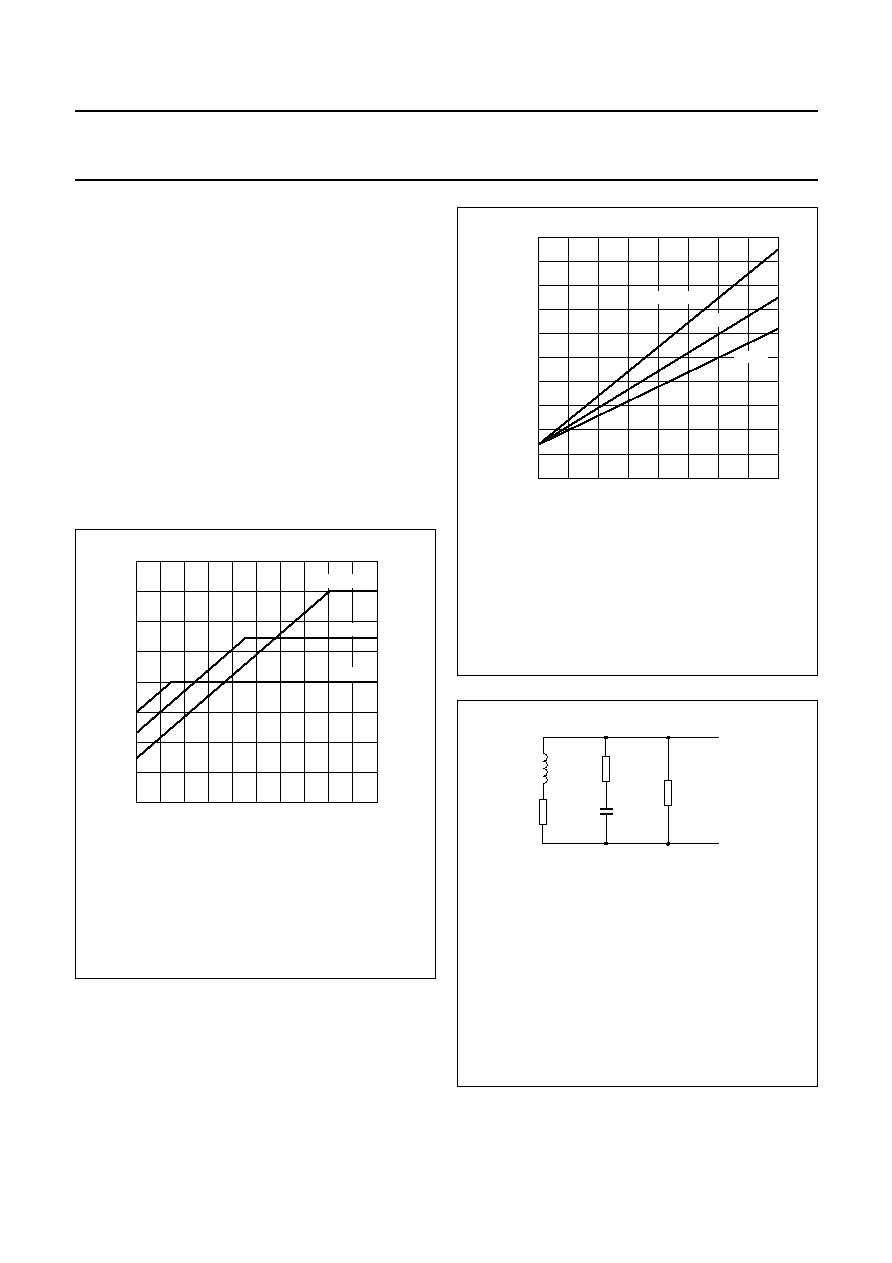
Fig.9
Maximum output swing on line as a function
of line current with the peripheral supply
current as a parameter; R15 = 392
;
R16 = 56
.
As different values of R15 and R16 are allowed, different curves
would then apply
handbook, halfpage
10
8
4
6
2
0
20
30
MGR064
Iline (mA)
VLN(p-p)
(V)
Ip = 4 mA
2 mA
0 mA
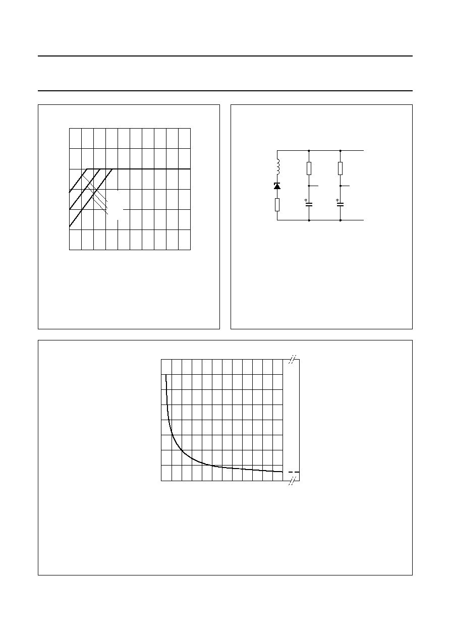
Fig.10 Curves showing the typical voltage drop
between LN and SLPE as a function of the
supply current for peripherals with R15 as a
parameter: V
CC2-SLPE
= 3.3 V (R
VA
not
connected).
V
CC2-SLPE
can be adjusted between approximately 3.3 and 4.3 V by
changing the value of R
VA
, this results in a parallel-shift of the curves.
The total voltage drop V
LN
V
LN-SLPE
+
([I
line
-
1.55 mA]
◊
R9).
handbook, halfpage
0
1
2
4
5.5
3.0
5.0
MGR065
3
4.0
4.5
3.5
Ip (mA)
VLN-SLPE
(V)
R15 = 511
392
301
Fig.11 Equivalent impedance between LN and
V
EE
at f
>
300 Hz in the application with
stabilized supply voltage for peripheral
circuits.
R
eq
R
p
R15
R16
-----------
1
+
=
L
eq
C3
R9
◊
R
eq
with R
p
15 k
=
◊
=
handbook, halfpage
MGR066
R9
20
LN
C3
470 nF
Req
Leq
VEE
R1
620
March 1994
11
Philips Semiconductors
Product specification
Low voltage versatile telephone transmission circuit
with dialler interface and transmit level dynamic limiting
TEA1064A
Microphone inputs MIC
+
and MIC
-
and gain pins
GAS1 and GAS2
The TEA1064A has symmetrical microphone inputs, its
input impedance is 64 k
(2
◊
32 k
) and its voltage
amplification is typ. 52 dB with R7 = 68 k
. Either
dynamic, magnetic or piezo-electric microphones can be
used, or an electret microphone with a built-in FET buffer.
Arrangements for the microphone types are shown in
Fig.12.
The gain of the microphone amplifier is proportional to
external resistor R7 connected between GAS1 and GAS2
and with this it can be adjusted between 44 dB and 52 dB
to suit the sensitivity of the transducer.
An external 100 pF capacitor (C6) is required between
GAS1 and SLPE to ensure stability. A larger value of C6
may be chosen to obtain a first-order low-pass filter with a
cut-off frequency corresponding to the time constant
R7
◊
C6.
Fig.12 Microphone arrangements: a) magnetic or dynamic microphone, the resistor (1) may be connected to
reduce the terminating impedance, or for sensitive types a resistive attenuator can be used to prevent
overloading the microphone inputs; b) electret microphone; c) piezo-electric microphone.
handbook, full pagewidth
MGR067
VEE
VCC1
16
8
9
11
9
8
(1)
(a)
(b)
(c)
MIC
+
MIC
-
MIC
-
MIC
+
9
8
MIC
-
MIC
+
Dynamic limiter (microphone) pin DLS/MMUTE
A low level at the DLS/MMUTE pin inhibits the microphone
inputs MIC
+
and MIC
-
but has no influence on the
receiving and DTMF amplifiers.
Removing the low level at the DLS/MMUTE pin provides
the normal function of the microphone amplifier after a
short time determined by the capacitor connected to
DLS/MMUTE pin. The microphone mute function can be
realised by a simple switch as shown in Fig.13.
To prevent distortion of the transmitted signal, the gain of
the sending amplifier is reduced rapidly when peaks of the
signal on the line exceed an internally-determined
threshold. The time in which gain reduction is effected
(attack time) is very short. The circuit stays in the
gain-reduced condition until the peaks of the sending
signal remain below the threshold level. The sending gain
then returns to normal after a time determined by the
capacitor connected to DLS/MMUTE (release time).
The internal threshold adapts automatically to the DC
voltage setting of the circuit (voltage V
LN-SLPE
). This
means that the maximum output swing on the line will be
higher if the DC voltage dropped across the circuit is
increased.
Fig.14 shows the maximum possible output swing on the
line as a function of the DC voltage drop (V
LN-SLPE
) with
I
line
-
I
p
as a parameter.
Fig.13 Microphone-mute function.
handbook, halfpage
MGR068
R17
3.3 k
7
11
DLS/MMUTE
VEE
March 1994
12
Philips Semiconductors
Product specification
Low voltage versatile telephone transmission circuit
with dialler interface and transmit level dynamic limiting
TEA1064A
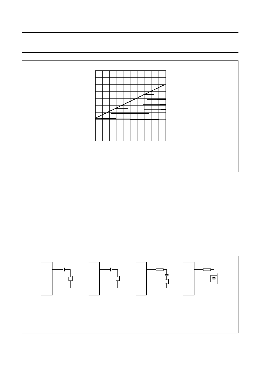
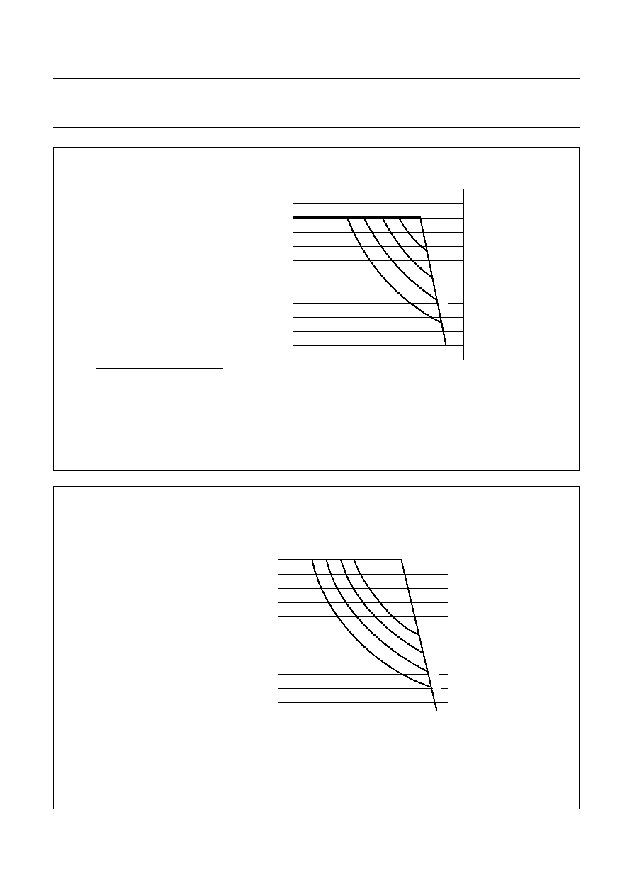
Fig.14 Maximum output swing on line as a function of the DC voltage drop V
LN-SLPE
with l
line
-
I
p
as a parameter:
R15 = 392
; R16 = 56
; or R15 = 0
and R16 = 392
+
56 = 448
.
handbook, full pagewidth
5.5
11
13
15
17
19
21
23
25
10
0
3
3.5
4
4.5
5
2
4
6
8
VLN(p-p)
(V)
VLN-VSLPE (V)
Iline-Ip
(mA)
MGR069
The internal threshold level is lowered automatically if the
DC current in the transmit output stage is insufficient. This
prevents distortion of the sending signal in applications
using parallel-connected telephones or telephones
operating over long lines, for example.
Dynamic limiting also considerably improves sidetone
performance in over-drive conditions (less distortion;
limited sidetone level).
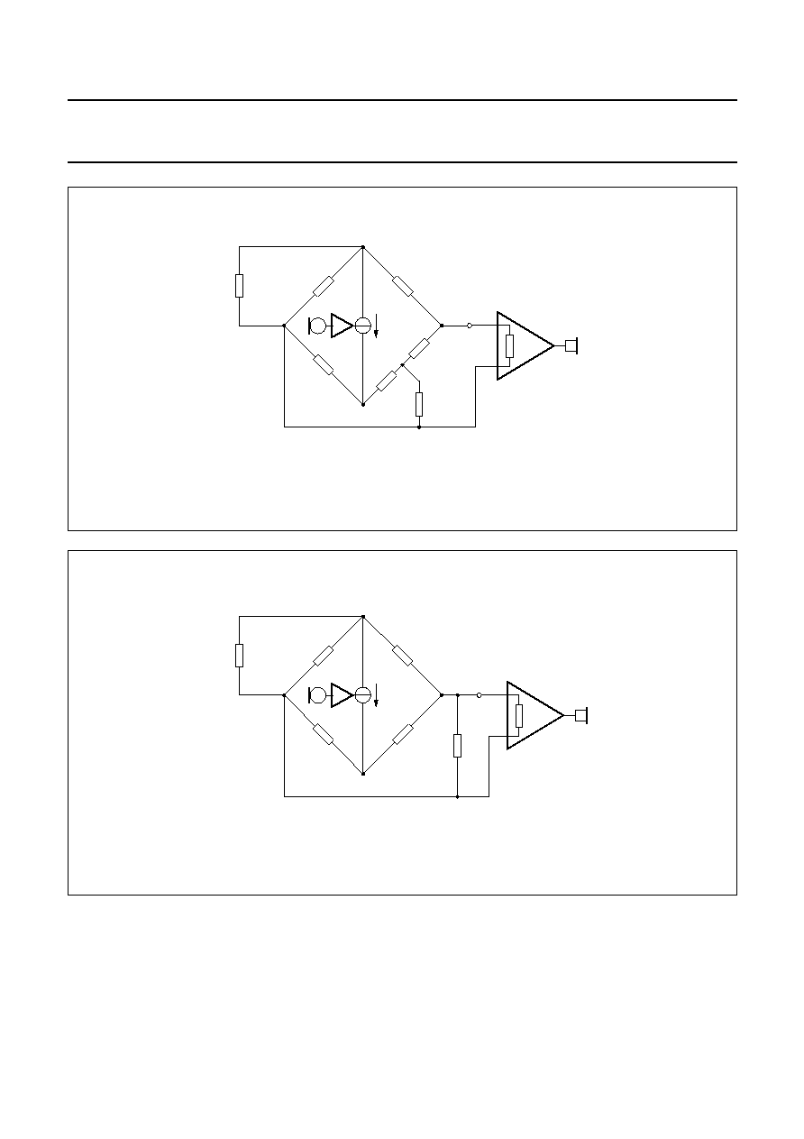
Receiving amplifier IR, QR
+
, QR
-
and GAR
The receiving amplifier has one input IR and two
complementary outputs, QR
+
(non-inverting) and QR
-
(inverting). These outputs may be used for single-ended or
differential drive, depending on the type and sensitivity of
the earpiece used (see Fig.15). Gain from IR to QR
+
is
typically 31 dB with R4 = 100 k
, sufficient for
low-impedance magnetic or dynamic earpieces which are
suitable for single-ended drive. By using both outputs
(differential drive) the gain is increased by 6 dB.
Differential drive can be used when the earpiece
impedance exceeds 450
as with high-impedance
dynamic, magnetic or piezo-electric earpieces.
Fig.15 Alternative receiver arrangements: a) dynamic earpiece with an impedance less than 450
; b) dynamic
earpiece with an impedance more than 450
; c) magnetic earpiece with an impedance more than 450
,
resistor (1) may be connected to prevent distortion (inductive load); d) piezo-electric earpiece, resistor (2)
is required to increase the phase margin (stability with capacitive load).
handbook, full pagewidth
MGR070
(1)
QR
-
QR
+
5
4
VEE
11
QR
-
QR
+
5
4
QR
-
QR
+
5
4
(2)
QR
-
QR
+
5
4
(a)
(b)
(c)
(d)
March 1994
13
Philips Semiconductors
Product specification
Low voltage versatile telephone transmission circuit
with dialler interface and transmit level dynamic limiting
TEA1064A
The output voltage of the receiving amplifier is specified for
continuous-wave drive. Fig.16 shows the maximum output
swing of the receiving amplifier as a function of the DC
voltage drop (V
LN
). The maximum output voltage will be
higher under speech conditions, where the ratio of the
peak to the RMS value is higher.
The gain of the receiving amplifier can be adjusted to suit
the sensitivity of the transducer used. The adjustment
range is between 20 dB and 39 dB with single-ended drive
and between 26 dB and 45 dB with differential drive. The
gain is proportional to the external resistor R4 connected
between GAR and QR
+
. The overall gain between LN and
QR
+
can be found by subtracting the attenuation of the
anti-sidetone network (32 dB) from the amplifier gain.
Two external capacitors (C4 =100 pF and
C7 = 10
◊
C4 = 1 nF) ensure stability. A larger value may
be chosen to obtain a first-order low-pass filter. The cut-off
frequency corresponds with the time constant R4
◊
C4.
The relationship C7 = 10
◊
C4 must be maintained.
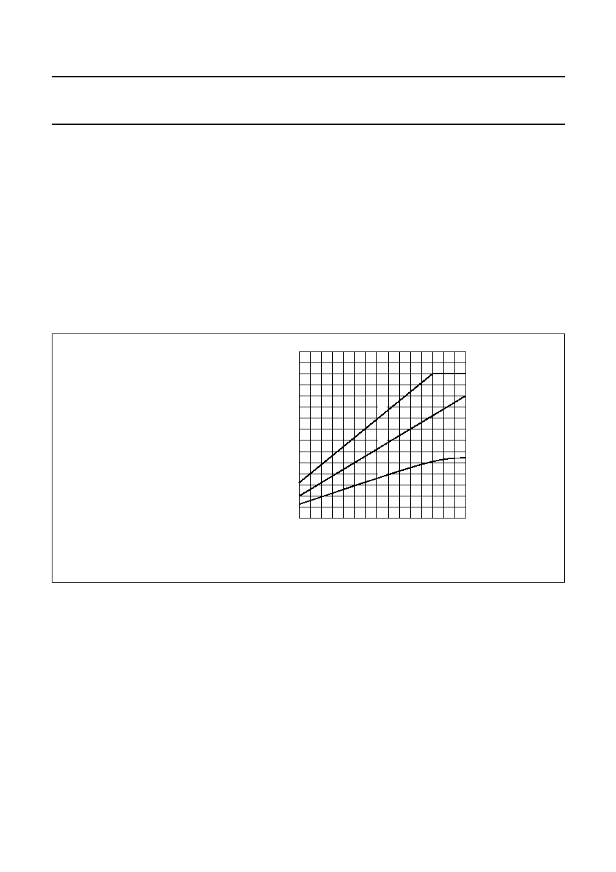
Fig.16 Maximum output swing of the receiving amplifier as a function of DC voltage drop V
LN
with the load at the
receiver output as parameter: valid for both supply options; THD = 2%; I
line
= 15 mA.
Curve (1) is for a differential load of 47 nF (series
resistance = 100
); f = 3400 Hz.
Curve (2) is for a differential load of 450
; f = 1 kHz.
Curve (3) is for a single-ended load of 150
; f = 1 kHz.
handbook, halfpage
0
3
4
6
1.5
0.5
1.0
MGR071
5
VLN (V)
VQR(rms)
(V)
(2)
(3)
(1)
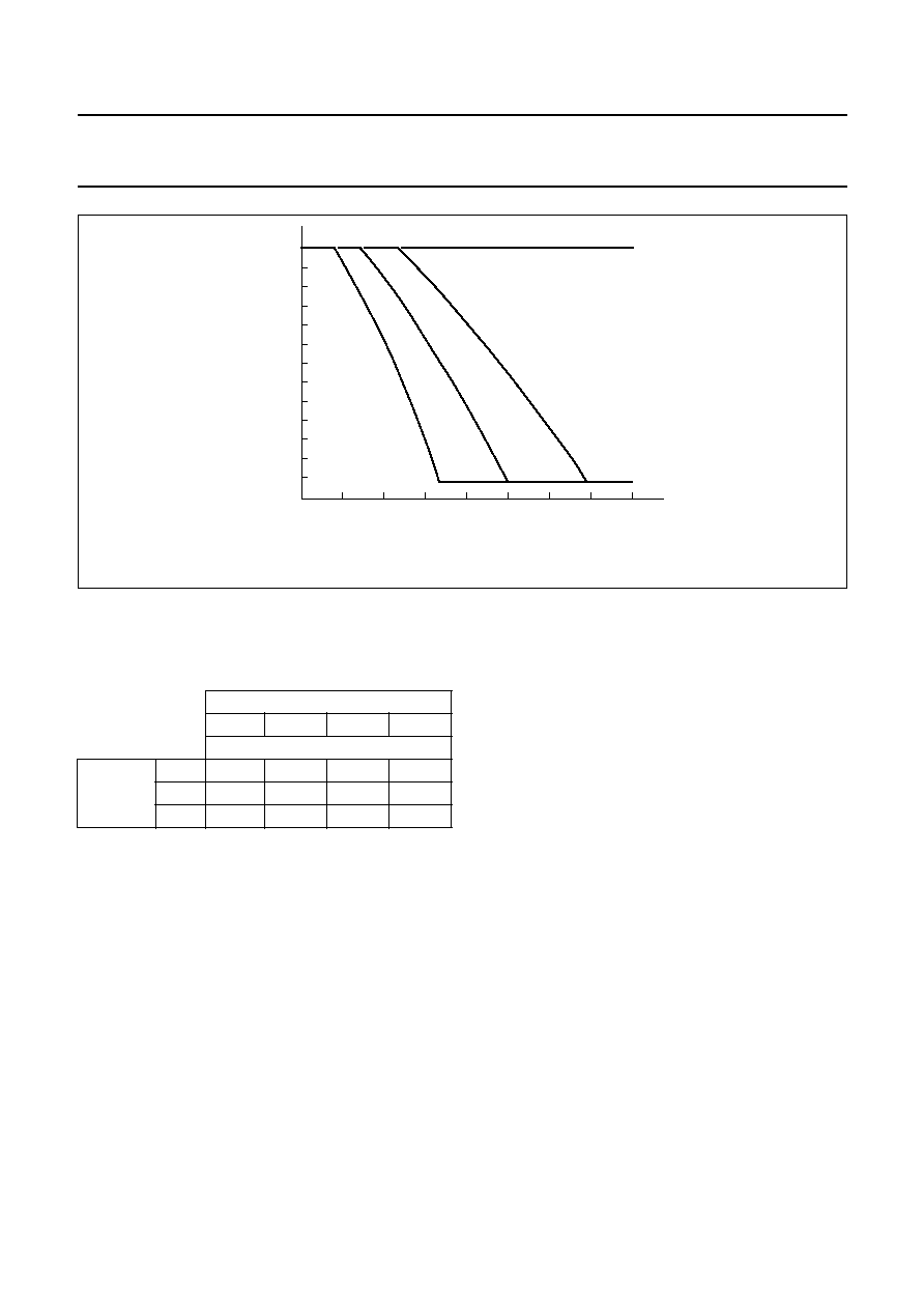
Automatic gain control input AGC
Automatic compensation of line loss is obtained by
connecting a resistor (R6) between AGC and V
EE
. This
automatic gain control varies the gain of the microphone
amplifier and receiving amplifier in accordance with the DC
line current. The control range is 6.1 dB; this corresponds
to a 5 km line of 0.5 mm diameter copper twisted-pair
cable (DC resistance = 176
/km, average
attenuation = 1.2 dB/km). The DTMF gain is not affected
by this feature.
The value of R6 must be chosen with reference to the
exchange supply voltage and its feeding bridge resistance
(see Fig.17 and Table 1). Different values of R6 give the
same line current ratios at the start and the end of the
control range. If automatic line-loss compensation is not
required the AGC pin can be left open, the amplifiers then
give their maximum gain.
March 1994
14
Philips Semiconductors
Product specification
Low voltage versatile telephone transmission circuit
with dialler interface and transmit level dynamic limiting
TEA1064A
Fig.17 Variation of gain as a function of line current with R6 as a parameter; R9 = 20
.
handbook, full pagewidth
MGR072
-
6
-
5
-
4
-
3
-
2
-
1
0
Avd
(dB)
Iline (mA)
80
90
60
70
40
50
20
30
10
93.1 k
66.5 k
R6 =
R6 =
118 k
Table 1
Values of R6 giving optimum line-loss
compensation at various values of exchange
supply voltage (V
exch
) and exchange feeding
bridge resistance (R
exch
); R9 = 20
.
MUTE input (see notes 1. and 2.)
MUTE = HIGH enables the DTMF input and inhibits the
microphone and receiving amplifier inputs.
MUTE = LOW or open-circuit disables the DTMF input and
enables the microphone and receiving amplifier inputs.
Switching MUTE gives negligible clicks at the telephone
outputs and on the line.
Dual-tone multi-frequency input DTMF (see note 1.)
When the DTMF input is enabled, dialling tones may be
sent on to the line. The voltage gain between DTMF-SLPE
and LN-V
EE
is typ. 26 dB less than the gain of the
microphone amplifier and varies with R7 in the same way
as the gain of the microphone amplifier. This means that
the tone level at the DTMF input has to be adjusted after
R
exch
(
)
400
600
800
1000
R6 (k
)
V
exch
(V)
36
84.5
66.5
X
X
48
118
93.1
77.8
66.5
60
X
X
97.6
84.5
setting the gain of the microphone amplifier. With
R7 = 68 k
the gain is typically 26 dB.
The signalling tones can be heard in the earpiece at a low
level (confidence tone).
Power-down input PD (see notes 1. and 2.)
During pulse dialling or register recall (timed loop break)
the telephone line is interrupted; as a consequence it
provides no supply for the transmission circuit connected
to V
CC1
or for the peripherals between V
CC2
and SLPE.
These supply gaps are bridged by the charges in the
capacitors C1 and C15. The requirements on these
capacitors are eased by applying a HIGH level to the PD
input during the time of the loop break. This reduces the
internal supply current I
CC1
from (typ.) 1.3 mA to (typ.)
60
µ
A and switches off the voltage regulator to prevent
discharge via LN and V
CC2
.
A HIGH level at PD also internally disconnects the
capacitor at REG so that the voltage stabilizer has no
switch-on delay after line interruptions. This minimizes the
contribution of the IC to the current waveform during pulse
dialling or register recall.
When the power-down facility is not required, the PD pin
can be left open-circuit or connected to SLPE.
Side-tone suppression
Suppression of the transmitted signal in the earpiece is
obtained by the anti-sidetone network comprising R1//Z
line
,

March 1994
15
Philips Semiconductors
Product specification
Low voltage versatile telephone transmission circuit
with dialler interface and transmit level dynamic limiting
TEA1064A
R2, R3, R8, R9 and Z
bal
(see Fig.18). Maximum
compensation is obtained when the following conditions
are fulfilled:
a) R9
◊
R2 = R1
◊
(R3
+
[R8//Z
bal
])
b) (Z
bal
/[Z
bal
+
R8]) = (Z
line
/[Z
line
+
R1])
If fixed values are chosen for R1, R2, R3 and R9, then
condition a) is always fulfilled provided
R8//Z
bal
<< R3.
To obtain optimum sidetone suppression, condition b) has
to be fulfilled, resulting in:
Z
bal
= (R8/R1)
◊
Z
line
= k
◊
Z
line
where k is a scale factor; k = (R8/R1).
The scale factor k (value of R8) is chosen to meet the
following criteria:
∑
compatibility with a standard capacitor from the E6 or
E12 range for Z
bal
;
∑
Z
bal
//R8
<< R3 to fulfil condition a) and thus ensure
correct anti-sidetone bridge operation;
∑
Z
bal
+
R8
>> R9 to avoid influencing the transmit gain.
In practice Z
line
varies considerably with the line length and
line type. Therefore the value chosen for Z
bal
should be for
an average line length giving satisfactory sidetone
suppression with short and long lines. The suppression
also depends on the accuracy of the match between
Z
bal
and the impedance of the average line.
Example
The line impedance for which optimum suppression is to
be obtained can be represented by
210
+
(1265
// 140 nF). This represents a 5 km line of
0.5 mm diameter copper twisted-pair cable matched with
600
(176
/km; 38 nF/km).
With k = 0.64 this results in: R8 = 390
;
Z
bal
= 130
+
(820
// 220 nF).
The anti-sidetone network for the TEA1060 family shown
in Fig.18 attenuates the signal received from the line by
32 dB before it enters the receiving amplifier. The
attenuation is almost constant over the whole
audio-frequency range.
Alternatively a conventional Wheatstone bridge can be
used as an anti-sidetone circuit (Fig.19). Both bridge types
can be used with either resistive or complex set
impedances. (More information on the balancing of
anti-sidetone bridges can be obtained in our publication
"Versatile speech transmission ICs for electronic
telephone sets", order number 9398 341 10011).
Notes
1. The reference used for the MUTE, DTMF and PD
inputs is SLPE.
2. A LOW level for any of these pins is defined by
connection to SLPE, a HIGH level is defined as a
voltage greater than V
SLPE
+
1.5 V and smaller than
V
CC1
+
0.4 V.
March 1994
16
Philips Semiconductors
Product specification
Low voltage versatile telephone transmission circuit
with dialler interface and transmit level dynamic limiting
TEA1064A
Fig.18 Equivalent circuit of TEA1060 family anti-side-tone bridge.
handbook, full pagewidth
MGR073
R1
R2
R9
R3
IR
R8
VEE
SLPE
LN
Zline
Rt
im
Zbal
Fig.19 Equivalent circuit of an anti-sidetone network in the Wheatstone bridge configuration.
handbook, full pagewidth
MGR074
R1
R9
IR
R8
VEE
SLPE
LN
Zline
Rt
im
RA
Zbal

March 1994
17
Philips Semiconductors
Product specification
Low voltage versatile telephone transmission circuit
with dialler interface and transmit level dynamic limiting
TEA1064A
RATINGS
Limiting values in accordance with the Absolute Maximum System (IEC 134)
Notes
1. Mostly dependent on the maximum required T
amb
and on the voltage between LN and SLPE. See Figs 20 and 21 to
determine the current as a function of the required voltage and the temperature.
2. Calculated for the maximum ambient temperature specified T
amb
= 75
∞
C and a maximum junction temperature of
125
∞
C.
THERMAL RESISTANCE
PARAMETER
CONDITIONS
SYMBOL
MIN.
MAX.
UNIT
Positive line voltage continuous
V
LN
-
12
V
Repetitive line voltage during
switch-on line interruption
V
LN
-
13.2
V
Repetitive peak line voltage
one 1 ms pulse per 5 s
R9 = 20
;
R10 = 13
(Fig.24)
V
LN
-
28
V
Line current TEA1064A (note 1)
R9 = 20
I
LN
-
140
mA
Line current TEA1064AT (note 1)
R9 = 20
I
LN
-
140
mA
Input voltage on pins other than
LN and V
CC2
V
i
V
EE
-
0.7
V
CC1
+
0.7
V
Total power dissipation (note 2)
R9 = 20
TEA1064A
P
tot
-
714
mW
TEA1064AT
P
tot
-
555
mW
Storage temperature range
T
stg
-
40
+
125
∞
C
Operating ambient temperature range
T
amb
-
25
+
75
∞
C
Junction temperature
T
j
-
+
125
∞
C
From junction to ambient in free air
TEA1064A
R
th j-a
=
70 K/W
TEA1064AT mounted on glass epoxy board 41
◊
19
◊
1.5 mm
R
th j-a
=
90 K/W
March 1994
18
Philips Semiconductors
Product specification
Low voltage versatile telephone transmission circuit
with dialler interface and transmit level dynamic limiting
TEA1064A
Fig.20 TEA1064A safe operating area.
T
amb
P
tot
(1)
45
∞
C
1143 mW
(2)
55
∞
C
1000 mW
(3)
65
∞
C
857 mW
(4)
75
∞
C
714 mW
handbook, halfpage
2
12
160
40
80
120
60
100
140
MGR075
4
6
8
10
VLN-VSLPE (V)
(2)
(3)
(4)
(1)
ILN
(mA)
Fig.21 TEA1064AT safe operating area.
T
amb
P
tot
(1)
45
∞
C
888 mW
(2)
55
∞
C
777 mW
(3)
65
∞
C
666 mW
(4)
75
∞
C
555 mW
handbook, halfpage
2
12
150
30
70
110
50
90
130
MSA546
4
6
8
10
VLN-VSLPE (V)
(2)
(3)
(4)
(1)
ILN
(mA)

March 1994
19
Philips Semiconductors
Product specification
Low voltage versatile telephone transmission circuit
with dialler interface and transmit level dynamic limiting
TEA1064A
CHARACTERISTICS
I
line
= 11 to 140 mA; V
EE
= 0 V; f = 800 Hz; T
amb
= 25
∞
C; R
L
= 600
; tested in the circuit of Fig.22 or 23); unless
otherwise specified
PARAMETER
CONDITIONS
SYMBOL
MIN.
TYP.
MAX.
UNIT
Supplies LN, V
CC1
, V
CC2
(pins 1, 16, 19)
Reference DC voltage between
V
CC2
and SLPE
I
line
= 15 mA
I
p
= 0; 4 mA
R
VA
not connected
V
CC2-SLPE
3.05
3.3
3.55
V
Variation with temperature
I
line
= 15 mA
V
CC2-SLPE
/
T
-
3.0
-
1.0
1.0
mV/K
Variation with line current referred
to 15 mA
I
line
= 100 mA
V
CC2-SLPE
-
60
-
mV
With R
VA
connected between
REG and SLPE
R
VA
= 33 k
V
CC2-SLPE
3.6
3.8
4.2
V
R
VA
= 20 k
V
CC2-SLPE
3.95
4.2
4.65
V
DC line voltage:
voltage drop between LN and V
EE
MIC
-
, MIC
+
inputs open;
R15 = 392
;
without R
VA
at I
line
= 15 mA
I
p
= 0 mA
V
LN
3.4
3.6
4.0
V
I
p
= 2 mA
V
LN
4.2
4.4
4.8
V
I
p
= 4 mA
V
LN
4.9
5.1
5.5
V
at I
line
= 100 mA
I
p
= 2 mA
V
LN
-
6.1
7.0
V
at I
line
= 140 mA
Ip = 2 mA
V
LN
-
7.0
7.8
V
Voltage drop under low current
conditions
I
p
= 0 mA
I
line
= 2 mA
V
LN
-
1.8
-
V
I
line
= 4 mA
V
LN
-
2.2
-
V
I
line
= 7 mA
V
LN
-
3.2
-
V
I
line
= 11 mA
V
LN
-
3.5
-
V
Internal supply current I
CC1
:
current into pin V
CC1
V
CC1
= 2.8 V
PD = LOW
I
CC1
-
1.3
1.6
mA
PD = HIGH
I
CC1
-
60
82
µ
A
Microphone inputs MIC
-
, MIC
+
(pins 8, 9)
Input impedance:
differential
Z
i
51
64
77
k
single-ended
Z
i
25.5
32.0
38.5
k
Common mode rejection ratio
CMRR
-
82
-
dB

March 1994
20
Philips Semiconductors
Product specification
Low voltage versatile telephone transmission circuit
with dialler interface and transmit level dynamic limiting
TEA1064A
Voltage gain (see Fig.22)
I
line
= 15 mA;
R7 = 68 k
G
v
51
52
53
dB
Variation of G
v
with frequency,
referred to 0.8 kHz
f = 300 and 3400 Hz
G
v
f
-
0.5
±
0.1
+
0.5
dB
Variation of G
v
with temperature,
referred to 25
∞
C
without R6;
I
line
= 50 mA;
T
amb
=
-
25 to
+
75
∞
C
G
v
T
-
±
0.2
-
dB
DTMF input (pin 12)
Input impedance
Z
i
16.8
20.7
24.6
k
Voltage gain (see Fig.22)
I
line
= 15 mA;
R7 = 68 k
G
v
25
26
27
dB
Variation of G
v
with frequency,
referred to 0.8 kHz
f = 300 and 3400 Hz
G
v
f
-
0.5
±
0.1
+
0.5
dB
f = 697 and 1633 Hz
G
v
f
-
0.2
±
0.05
+
0.2
dB
Variation of G
v
with temperature,
referred to 25
∞
C
I
line
= 50 mA;
T
amb
=
-
25 to
+
75
∞
C
G
v
T
-
±
0.2
0.5
dB
Gain adjustment inputs GAS1, GAS2
(pins 2, 3)
Transmitting amplifier,
gain adjustment range
G
v
-
8
-
+
0
dB
Sending amplifier output LN (pin 1)
Dynamic limiter
Output voltage swing
(peak-to-peak value)
I
line
= 15 mA;
R7 = 68 k
;
I
p
= 0 mA;
V
i(rms)
= 3.6 mV
V
LN(p-p)
3.6
4.0
4.5
V
Total harmonic distortion
V
i
= 3.6 mV
+
10 dB
THD
-
1.5
2.0
%
V
i
= 3.6 mV
+
15 dB
THD
-
2.8
10.0
%
Output voltage swing
(peak-to-peak value)
V
i
= 3.6 mV
+
10 dB
I
p
= 2 mA
V
LN(p-p)
3.7
3.95
4.2
V
I
p
= 4 mA
V
LN(p-p)
3.0
3.25
3.5
V
I
p
= 0 mA;
I
line
= 7 mA
V
LN(p-p)
-
2
-
V
I
p
= 0 mA;
I
line
= 4 mA
V
LN(p-p)
-
1
-
V
PARAMETER
CONDITIONS
SYMBOL
MIN.
TYP.
MAX.
UNIT

March 1994
21
Philips Semiconductors
Product specification
Low voltage versatile telephone transmission circuit
with dialler interface and transmit level dynamic limiting
TEA1064A
Dynamic behaviour of limiter
C16 = 470 nF
attack time, V
mic
jumps from
2 mV to 40 mV
t
att
-
1.5
5.0
ms
release time, V
mic
jumps from
40 mV to 2 mV
t
rel
50
150
-
ms
Noise output voltage (RMS value)
l
line
= 15 mA;
R7 = 68 k
;
200
between
MIC
-
and MIC
+
;
psophometrically
weighted (P53 curve)
V
no(rms)
-
-
72
-
dBmp
Receiving amplifier input IR (pin 13)
Input impedance
Z
i
17
21
25
k
Receiving amplifier outputs QR
-
QR
+
(pins 4, 5)
Output impedance
single-ended
Z
o
-
4
-
Voltage gain
Fig.23;
I
line
= 15 mA;
R4 = 100 k
single-ended; R
T
= 300
G
v
30
31
32
dB
differential; R
T
= 600
G
v
36
37
38
dB
Variation with frequency,
referred to 0.8 kHz
f = 300 and 3400 Hz
G
v
f
-
0.5
-
0.2
0
dB
Variation with temperature,
referred to 25
∞
C
without R6;
I
line
= 50 mA;
T
amb
=
-
25 to
+
75
∞
C
G
v
T
-
±
0.2
-
dB
Output voltage (RMS value)
THD = 2%;
sinewave drive;
R4 = 100 k
;
I
line
= 15 mA
single-ended; R
T
= 150
I
p
= 0 mA
V
o(rms)
-
0.22
-
V
I
p
= 2 mA
V
o(rms)
-
0.35
-
V
differential; R
T
= 450
I
p
= 0 mA
V
o(rms)
-
0.39
-
V
I
p
= 2 mA
V
o(rms)
-
0.64
-
V
differential; C
T
= 47 nF;
(100
series resistor); f = 3400 Hz
I
p
= 0 mA
V
o(rms)
-
0.57
-
V
I
p
= 2 mA
V
o(rms)
-
0.9
-
V
PARAMETER
CONDITIONS
SYMBOL
MIN.
TYP.
MAX.
UNIT

March 1994
22
Philips Semiconductors
Product specification
Low voltage versatile telephone transmission circuit
with dialler interface and transmit level dynamic limiting
TEA1064A
Output voltage (RMS value)
I
p
= 0 mA;
THD = 10%;
sinewave drive;
R4 = 100 k
;
single-ended;
R
T
= 150
;
I
line
= 4 mA
V
o(rms)
-
25
-
mV
I
line
= 7 mA
V
o(rms)
-
160
-
mV
Noise output voltage (RMS value)
I
line
= 15 mA;
R
4
= 100 k
;
psophometrically
weighted
(P53 curve);
pin IR open
single-ended;
R
T
= 300
;
V
no(rms)
-
45
-
µ
V
differential;
R
T
= 600
V
no(rms)
-
90
-
µ
V
Noise output voltage (RMS value)
in circuit of Fig.23;
S1 in position 2;
200
between
MIC
+
and MIC
-
;
single-ended;
R
T
= 300
R
7
= 68 k
V
no(rms)
-
100
-
µ
V
R
7
= 24.9 k
V
no(rms)
-
65
-
µ
V
Gain adjustment input GAR (pin 6)
Receiving amplifier,
gain adjustment range
G
v
-
11
-
+
8
dB
MUTE INPUT (pin 14)
Input voltage HIGH
V
IH
1.5
+
V
SLPE
-
V
CC1
+
0.4
V
Input voltage LOW
V
IL
0
-
0.3
+
V
SLPE
V
Input current
I
mute
-
11
20
µ
A
Change of microphone amplifier
gain at mute-ON
MUTE = HIGH
-
G
v
-
100
-
dB
PARAMETER
CONDITIONS
SYMBOL
MIN.
TYP.
MAX.
UNIT

March 1994
23
Philips Semiconductors
Product specification
Low voltage versatile telephone transmission circuit
with dialler interface and transmit level dynamic limiting
TEA1064A
Voltage gain from input
DTMF-SLPE to QR
+
output
with mute-ON
MUTE = HIGH;
single-ended load;
R
L
= 300
G
v
-
-
18
-
dB
Power-down input PD (pin 15)
Input voltage HIGH
V
IH
1.5
+
V
SLPE
-
V
CC1
+
0.4
V
Input voltage LOW
V
IL
0
-
0.3
+
V
SLPE
V
Input current
I
PD
-
5
10
µ
A
Automatic gain control input AGC
(pin 18)
Controlling the gain from
IR (pin 13) to QR
+
, QR
-
(pins 4, 5) and the gain
from MIC
+
, MIC
-
(pins 8, 9)
to LN (pin 1)
R6 = 93.1 k
(between pins
18 and 11)
gain control range with respect to
I
line
= 15 mA
I
line
= 75 mA
-
G
v
5.7
6.1
6.5
dB
Highest line current
for maximum gain
I
line
-
24
-
mA
Lowest line current
for minimum gain
I
line
-
61
-
mA
Change of gain
between I
line
= 15 and 35 mA
-
G
v
0.9
1.4
1.9
dB
Microphone mute
input DLS/MMUTE (pin 7)
Input voltage low
V
IL
V
EE
-
V
EE
+
0.3
V
Input current at low
input voltage
I
IL
-
85
-
60
-
35
µ
A
Release time after a low
level on pin 7
C16 = 470 nF
t
rel
-
30
-
ms
Change of microphone amplifier
gain at low input voltage on
pin 7
-
G
v
-
100
-
dB
PARAMETER
CONDITIONS
SYMBOL
MIN.
TYP.
MAX.
UNIT

March 1994
24
Philips Semiconductors
Product specification
Low voltage versatile telephone transmission circuit
with dialler interface and transmit level dynamic limiting
TEA1064A
Fig.22 Test circuit for defining voltage gain of MIC
-
, MIC
+
and DTMF inputs; voltage gain (G
v
) is defined as
20 log
V
o
/ V
i
.
For measuring the gain from MIC
+
and MIC
-
the MUTE input should be LOW
or open-circuit; for measuring the DTMF input, the MUTE input should be HIGH.
Inputs not being tested should be open-circuit.
andbook, full pagewidth
MGR076
VCC1
LN
DLS/MMUTE
PD
MUTE
DTMF
MIC
-
MIC
+
IR
620
TEA1064A
R4
100
k
RL
600
Iline
C4
100 pF
C7 1 nF
11 to
140 mA
100
µ
F
7
C15
220
µ
F
C1
100
µ
F
Ip
15
14
12
8
9
13
20
C16
470 nF
R7
68
k
C6
100 pF
10
µ
F
392
R1
R15
QR
-
QR
+
GAR
GAS1
GAS2
4
16
VCC2
19
1
5
6
2
3
Vi
Vi
Vo
VEE
REG
AGC
STAB
R9
20
R6
18
17
11
10
R5
3.6
k
C3
470
nF
SLPE
R16
56
March 1994
25
Philips Semiconductors
Product specification
Low voltage versatile telephone transmission circuit
with dialler interface and transmit level dynamic limiting
TEA1064A
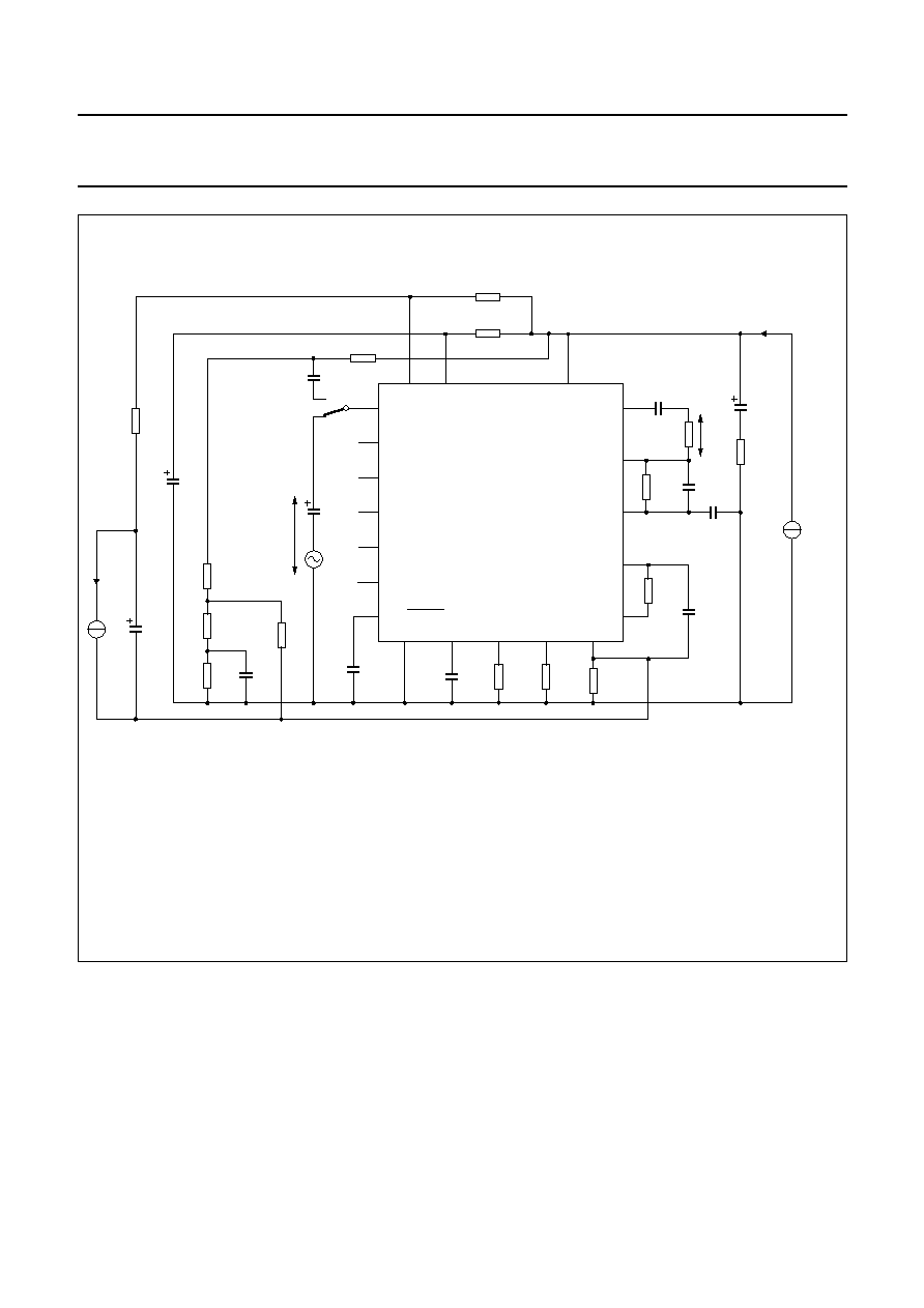
APPLICATION INFORMATION
The basic application circuit is shown in Fig.24 and some typical applications are shown in Figs 25, 26 and 27.
In the basic application, the circuit provides two possibilities for supplies to peripheral circuits:
∑
regulated line voltage V
LN
(stabilized V
LN-SLPE
) and unregulated supply voltage for peripheral circuits, the supply
voltage is dependent only on the peripheral supply current. This application is the same as that used for
TEA1060/TEA1061, TEA1067 and TEA1068;
∑
stabilized supply voltage for peripherals (V
CC2-SLPE
), the DC line voltage depends on the current flowing to the
peripheral circuits.
handbook, full pagewidth
MGR077
VEE
REG
AGC
STAB
VCC1
LN
R9
20
820
220
nF
R6
18
17
11
DLS/MMUTE
PD
MUTE
DTMF
MIC
-
MIC
+
IR
S1
620
TEA1064A
R4
100
k
RL
600
ZT
Vo
Iline
C4
100 pF
C7 1 nF
11 to
140 mA
100
µ
F
7
C15
220
µ
F
C1
100
µ
F
Ip
15
14
12
8
9
13
100 nF
2
1
10
20
R5
3.6
k
R3
3.92 k
R8
390
130
C3
470
nF
C16
470 nF
SLPE
R7
68
k
C6
100 pF
10
µ
F
130 k
R2
392
R1
R15
QR
-
QR
+
GAR
GAS1
GAS2
4
16
VCC2
19
1
5
6
2
3
Vi
10
µ
F
R16
56
Fig.23 Test circuit for defining voltage gain of the receiving amplifier, voltage gain (G
v
) is defined as
20 log
V
o
/ V
i
(with S1 in position 1).

March
1994
26
Philips Semiconductors
Product specification
Low voltage versatile telephone transmission circuit
with dialler interface and transmit level dynamic limiting
TEA1064A
This text is here in white to force landscape pages to be rotated correctly when browsing through the pdf in the Acrobat reader.This text is here in
_
white to force landscape pages to be rotated correctly when browsing through the pdf in the Acrobat reader.This text is here inThis text is here in
white to force landscape pages to be rotated correctly when browsing through the pdf in the Acrobat reader. white to force landscape pages to be ...
pagewidth
MGR078
VEE
REG
GAS2
GAS1
100 pF
AGC
STAB
LN
VCC1
VCC2
392
R15
620
R1
390
R8
R5
3.6
k
R9
20
R4
100 k
17
3
2
20
DLS/MMUTE
GAR
MIC
-
MIC
+
IR
TEA1064A
8
9
6
5
4
13
18
10
R6
R7
68
k
C16
470
nF
SLPE
C6
11
R17
3.3 k
R16
56
R14
R13
C5
100 nF
Zbal
C3
470
nF
C15
220
µ
F
C1
100
µ
F
-
+
C4
100 pF
C7
1 nF
R3
3.92 k
R2
130 k
R10
13
BAS11
(2
◊
)
BZW14
(2
◊
)
telephone
line
QR
-
QR
+
1
16
7
DTMF
MUTE
PD
12
14
15
from dial
and
control circuits
Fig.24 Basic application of the TEA1064A with stabilized supply for peripherals, shown here with a piezo-electric earpiece and DTMF dialling.
The diode bridge and R10 limit the current into, and the voltage across, the circuit during line transients. A different protection
arrangement is required for pulse dialling or register recall.

March 1994
27
Philips Semiconductors
Product specification
Low voltage versatile telephone transmission circuit
with dialler interface and transmit level dynamic limiting
TEA1064A
For the basic application giving regulated line voltage the above circuit is changed as follows:
-
R15 must be short-circuited;
-
the value of R16 is changed to 392
;
-
the value of C3 is changed to 4.7
µ
F.
Fig.25 Typical DTMF-pulse set application circuit (simplified) showing the TEA1064A with the CMOS bilingual
dialling circuit PCD3310; the broken line indicates optional flash (register recall by timed loop break).
handbook, full pagewidth
TEA1064A
telephone
line
cradle
contact
BST76A
VEE
SLPE
LN
VCC2
DTMF
MUTE
PD
PCD3310
VSS
VDD
DTMF
M
FL
MGR079
Fig.26 Typical pulse dial set application circuit (simplified) showing the TEA1064A with one of the PCD332X
family of CMOS interrupted current-loop dialling circuits.
handbook, full pagewidth
MGR080
TEA1064A
telephone
line
cradle
contact
BST76A
VEE
SLPE
LN
VCC2
DTMF
MUTE
PD
PCD332x
FAMILY
VSS
VDD
M
DP
DP/flash
March 1994
28
Philips Semiconductors
Product specification
Low voltage versatile telephone transmission circuit
with dialler interface and transmit level dynamic limiting
TEA1064A
Fig.27 Typical dual-standard (pulse and DTMF) feature phone application circuit (simplified) showing the
TEA1064A and the PCD3344 CMOS telephone microcontroller with on-chip DTMF generator plus
I
2
C-bus.
handbook, full pagewidth
MGR081
TEA1064A
telephone
line
cradle
contact
BST76A
VEE
SLPE
LN
VCC2
DTMF
MUTE
PD
PCD3344
PCF8577
VSS
VDD
TONE
M
DP
DP/flash
16-DIGIT
LCD
LCD MODULE
I
2
C-bus
March 1994
29
Philips Semiconductors
Product specification
Low voltage versatile telephone transmission circuit
with dialler interface and transmit level dynamic limiting
TEA1064A
PACKAGE OUTLINES
UNIT
A
max.
1
2
b
1
c
D
E
e
M
H
L
REFERENCES
OUTLINE
VERSION
EUROPEAN
PROJECTION
ISSUE DATE
IEC
JEDEC
EIAJ
mm
inches
DIMENSIONS (inch dimensions are derived from the original mm dimensions)
SOT146-1
92-11-17
95-05-24
A
min.
A
max.
b
Z
max.
w
M
E
e
1
1.73
1.30
0.53
0.38
0.36
0.23
26.92
26.54
6.40
6.22
3.60
3.05
0.254
2.54
7.62
8.25
7.80
10.0
8.3
2.0
4.2
0.51
3.2
0.068
0.051
0.021
0.015
0.014
0.009
1.060
1.045
0.25
0.24
0.14
0.12
0.01
0.10
0.30
0.32
0.31
0.39
0.33
0.078
0.17
0.020
0.13
SC603
M
H
c
(e )
1
M
E
A
L
seating plane
A
1
w
M
b
1
e
D
A
2
Z
20
1
11
10
b
E
pin 1 index
0
5
10 mm
scale
Note
1. Plastic or metal protrusions of 0.25 mm maximum per side are not included.
(1)
(1)
(1)
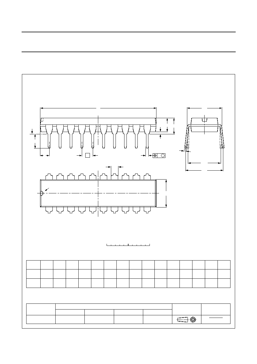
DIP20: plastic dual in-line package; 20 leads (300 mil)
SOT146-1

March 1994
30
Philips Semiconductors
Product specification
Low voltage versatile telephone transmission circuit
with dialler interface and transmit level dynamic limiting
TEA1064A
UNIT
A
max.
A
1
A
2
A
3
b
p
c
D
(1)
E
(1)
(1)
e
H
E
L
L
p
Q
Z
y
w
v
REFERENCES
OUTLINE
VERSION
EUROPEAN
PROJECTION
ISSUE DATE
IEC
JEDEC
EIAJ
mm
inches
2.65
0.30
0.10
2.45
2.25
0.49
0.36
0.32
0.23
13.0
12.6
7.6
7.4
1.27
10.65
10.00
1.1
1.0
0.9
0.4
8
0
o
o
0.25
0.1
DIMENSIONS (inch dimensions are derived from the original mm dimensions)
Note
1. Plastic or metal protrusions of 0.15 mm maximum per side are not included.
1.1
0.4
SOT163-1
10
20
w
M
b
p
detail X
Z
e
11
1
D
y
0.25
075E04
MS-013AC
pin 1 index
0.10
0.012
0.004
0.096
0.089
0.019
0.014
0.013
0.009
0.51
0.49
0.30
0.29
0.050
1.4
0.055
0.419
0.394
0.043
0.039
0.035
0.016
0.01
0.25
0.01
0.004
0.043
0.016
0.01
0
5
10 mm
scale
X
A
A
1
A
2
H
E
L
p
Q
E
c
L
v
M
A
(A )
3
A
SO20: plastic small outline package; 20 leads; body width 7.5 mm
SOT163-1
95-01-24
97-05-22

March 1994
31
Philips Semiconductors
Product specification
Low voltage versatile telephone transmission circuit
with dialler interface and transmit level dynamic limiting
TEA1064A
SOLDERING
Introduction
There is no soldering method that is ideal for all IC
packages. Wave soldering is often preferred when
through-hole and surface mounted components are mixed
on one printed-circuit board. However, wave soldering is
not always suitable for surface mounted ICs, or for
printed-circuits with high population densities. In these
situations reflow soldering is often used.
This text gives a very brief insight to a complex technology.
A more in-depth account of soldering ICs can be found in
our
"Data Handbook IC26; Integrated Circuit Packages"
(order code 9398 652 90011).
DIP
S
OLDERING BY DIPPING OR BY WAVE
The maximum permissible temperature of the solder is
260
∞
C; solder at this temperature must not be in contact
with the joint for more than 5 seconds. The total contact
time of successive solder waves must not exceed
5 seconds.
The device may be mounted up to the seating plane, but
the temperature of the plastic body must not exceed the
specified maximum storage temperature (T
stg max
). If the
printed-circuit board has been pre-heated, forced cooling
may be necessary immediately after soldering to keep the
temperature within the permissible limit.
R
EPAIRING SOLDERED JOINTS
Apply a low voltage soldering iron (less than 24 V) to the
lead(s) of the package, below the seating plane or not
more than 2 mm above it. If the temperature of the
soldering iron bit is less than 300
∞
C it may remain in
contact for up to 10 seconds. If the bit temperature is
between 300 and 400
∞
C, contact may be up to 5 seconds.
SO
R
EFLOW SOLDERING
Reflow soldering techniques are suitable for all SO
packages.
Reflow soldering requires solder paste (a suspension of
fine solder particles, flux and binding agent) to be applied
to the printed-circuit board by screen printing, stencilling or
pressure-syringe dispensing before package placement.
Several techniques exist for reflowing; for example,
thermal conduction by heated belt. Dwell times vary
between 50 and 300 seconds depending on heating
method. Typical reflow temperatures range from
215 to 250
∞
C.
Preheating is necessary to dry the paste and evaporate
the binding agent. Preheating duration: 45 minutes at
45
∞
C.
W
AVE SOLDERING
Wave soldering techniques can be used for all SO
packages if the following conditions are observed:
∑
A double-wave (a turbulent wave with high upward
pressure followed by a smooth laminar wave) soldering
technique should be used.
∑
The longitudinal axis of the package footprint must be
parallel to the solder flow.
∑
The package footprint must incorporate solder thieves at
the downstream end.
During placement and before soldering, the package must
be fixed with a droplet of adhesive. The adhesive can be
applied by screen printing, pin transfer or syringe
dispensing. The package can be soldered after the
adhesive is cured.
Maximum permissible solder temperature is 260
∞
C, and
maximum duration of package immersion in solder is
10 seconds, if cooled to less than 150
∞
C within
6 seconds. Typical dwell time is 4 seconds at 250
∞
C.
A mildly-activated flux will eliminate the need for removal
of corrosive residues in most applications.
R
EPAIRING SOLDERED JOINTS
Fix the component by first soldering two diagonally-
opposite end leads. Use only a low voltage soldering iron
(less than 24 V) applied to the flat part of the lead. Contact
time must be limited to 10 seconds at up to 300
∞
C. When
using a dedicated tool, all other leads can be soldered in
one operation within 2 to 5 seconds between
270 and 320
∞
C.
March 1994
32
Philips Semiconductors
Product specification
Low voltage versatile telephone transmission circuit
with dialler interface and transmit level dynamic limiting
TEA1064A
DEFINITIONS
LIFE SUPPORT APPLICATIONS
These products are not designed for use in life support appliances, devices, or systems where malfunction of these
products can reasonably be expected to result in personal injury. Philips customers using or selling these products for
use in such applications do so at their own risk and agree to fully indemnify Philips for any damages resulting from such
improper use or sale.
Data sheet status
Objective specification
This data sheet contains target or goal specifications for product development.
Preliminary specification
This data sheet contains preliminary data; supplementary data may be published later.
Product specification
This data sheet contains final product specifications.
Limiting values
Limiting values given are in accordance with the Absolute Maximum Rating System (IEC 134). Stress above one or
more of the limiting values may cause permanent damage to the device. These are stress ratings only and operation
of the device at these or at any other conditions above those given in the Characteristics sections of the specification
is not implied. Exposure to limiting values for extended periods may affect device reliability.
Application information
Where application information is given, it is advisory and does not form part of the specification.

March 1994
33
Philips Semiconductors
Product specification
Low voltage versatile telephone transmission circuit
with dialler interface and transmit level dynamic limiting
TEA1064A
NOTES

March 1994
34
Philips Semiconductors
Product specification
Low voltage versatile telephone transmission circuit
with dialler interface and transmit level dynamic limiting
TEA1064A
NOTES

March 1994
35
Philips Semiconductors
Product specification
Low voltage versatile telephone transmission circuit
with dialler interface and transmit level dynamic limiting
TEA1064A
NOTES

Internet: http://www.semiconductors.philips.com
Philips Semiconductors ≠ a worldwide company
© Philips Electronics N.V. 1998
SCA60
All rights are reserved. Reproduction in whole or in part is prohibited without the prior written consent of the copyright owner.
The information presented in this document does not form part of any quotation or contract, is believed to be accurate and reliable and may be changed
without notice. No liability will be accepted by the publisher for any consequence of its use. Publication thereof does not convey nor imply any license
under patent- or other industrial or intellectual property rights.
Middle East: see Italy
Netherlands: Postbus 90050, 5600 PB EINDHOVEN, Bldg. VB,
Tel. +31 40 27 82785, Fax. +31 40 27 88399
New Zealand: 2 Wagener Place, C.P.O. Box 1041, AUCKLAND,
Tel. +64 9 849 4160, Fax. +64 9 849 7811
Norway: Box 1, Manglerud 0612, OSLO,
Tel. +47 22 74 8000, Fax. +47 22 74 8341
Pakistan: see Singapore
Philippines: Philips Semiconductors Philippines Inc.,
106 Valero St. Salcedo Village, P.O. Box 2108 MCC, MAKATI,
Metro MANILA, Tel. +63 2 816 6380, Fax. +63 2 817 3474
Poland: Ul. Lukiska 10, PL 04-123 WARSZAWA,
Tel. +48 22 612 2831, Fax. +48 22 612 2327
Portugal: see Spain
Romania: see Italy
Russia: Philips Russia, Ul. Usatcheva 35A, 119048 MOSCOW,
Tel. +7 095 755 6918, Fax. +7 095 755 6919
Singapore: Lorong 1, Toa Payoh, SINGAPORE 319762,
Tel. +65 350 2538, Fax. +65 251 6500
Slovakia: see Austria
Slovenia: see Italy
South Africa: S.A. PHILIPS Pty Ltd., 195-215 Main Road Martindale,
2092 JOHANNESBURG, P.O. Box 7430 Johannesburg 2000,
Tel. +27 11 470 5911, Fax. +27 11 470 5494
South America: Al. Vicente Pinzon, 173, 6th floor,
04547-130 S√O PAULO, SP, Brazil,
Tel. +55 11 821 2333, Fax. +55 11 821 2382
Spain: Balmes 22, 08007 BARCELONA,
Tel. +34 93 301 6312, Fax. +34 93 301 4107
Sweden: Kottbygatan 7, Akalla, S-16485 STOCKHOLM,
Tel. +46 8 5985 2000, Fax. +46 8 5985 2745
Switzerland: Allmendstrasse 140, CH-8027 ZÐRICH,
Tel. +41 1 488 2741 Fax. +41 1 488 3263
Taiwan: Philips Semiconductors, 6F, No. 96, Chien Kuo N. Rd., Sec. 1,
TAIPEI, Taiwan Tel. +886 2 2134 2865, Fax. +886 2 2134 2874
Thailand: PHILIPS ELECTRONICS (THAILAND) Ltd.,
209/2 Sanpavuth-Bangna Road Prakanong, BANGKOK 10260,
Tel. +66 2 745 4090, Fax. +66 2 398 0793
Turkey: Talatpasa Cad. No. 5, 80640 GÐLTEPE/ISTANBUL,
Tel. +90 212 279 2770, Fax. +90 212 282 6707
Ukraine: PHILIPS UKRAINE, 4 Patrice Lumumba str., Building B, Floor 7,
252042 KIEV, Tel. +380 44 264 2776, Fax. +380 44 268 0461
United Kingdom: Philips Semiconductors Ltd., 276 Bath Road, Hayes,
MIDDLESEX UB3 5BX, Tel. +44 181 730 5000, Fax. +44 181 754 8421
United States: 811 East Arques Avenue, SUNNYVALE, CA 94088-3409,
Tel. +1 800 234 7381
Uruguay: see South America
Vietnam: see Singapore
Yugoslavia: PHILIPS, Trg N. Pasica 5/v, 11000 BEOGRAD,
Tel. +381 11 625 344, Fax.+381 11 635 777
For all other countries apply to: Philips Semiconductors,
International Marketing & Sales Communications, Building BE-p, P.O. Box 218,
5600 MD EINDHOVEN, The Netherlands, Fax. +31 40 27 24825
Argentina: see South America
Australia: 34 Waterloo Road, NORTH RYDE, NSW 2113,
Tel. +61 2 9805 4455, Fax. +61 2 9805 4466
Austria: Computerstr. 6, A-1101 WIEN, P.O. Box 213, Tel. +43 160 1010,
Fax. +43 160 101 1210
Belarus: Hotel Minsk Business Center, Bld. 3, r. 1211, Volodarski Str. 6,
220050 MINSK, Tel. +375 172 200 733, Fax. +375 172 200 773
Belgium: see The Netherlands
Brazil: see South America
Bulgaria: Philips Bulgaria Ltd., Energoproject, 15th floor,
51 James Bourchier Blvd., 1407 SOFIA,
Tel. +359 2 689 211, Fax. +359 2 689 102
Canada: PHILIPS SEMICONDUCTORS/COMPONENTS,
Tel. +1 800 234 7381
China/Hong Kong: 501 Hong Kong Industrial Technology Centre,
72 Tat Chee Avenue, Kowloon Tong, HONG KONG,
Tel. +852 2319 7888, Fax. +852 2319 7700
Colombia: see South America
Czech Republic: see Austria
Denmark: Prags Boulevard 80, PB 1919, DK-2300 COPENHAGEN S,
Tel. +45 32 88 2636, Fax. +45 31 57 0044
Finland: Sinikalliontie 3, FIN-02630 ESPOO,
Tel. +358 9 615800, Fax. +358 9 61580920
France: 51 Rue Carnot, BP317, 92156 SURESNES Cedex,
Tel. +33 1 40 99 6161, Fax. +33 1 40 99 6427
Germany: Hammerbrookstraþe 69, D-20097 HAMBURG,
Tel. +49 40 23 53 60, Fax. +49 40 23 536 300
Greece: No. 15, 25th March Street, GR 17778 TAVROS/ATHENS,
Tel. +30 1 4894 339/239, Fax. +30 1 4814 240
Hungary: see Austria
India: Philips INDIA Ltd, Band Box Building, 2nd floor,
254-D, Dr. Annie Besant Road, Worli, MUMBAI 400 025,
Tel. +91 22 493 8541, Fax. +91 22 493 0966
Indonesia: PT Philips Development Corporation, Semiconductors Division,
Gedung Philips, Jl. Buncit Raya Kav.99-100, JAKARTA 12510,
Tel. +62 21 794 0040 ext. 2501, Fax. +62 21 794 0080
Ireland: Newstead, Clonskeagh, DUBLIN 14,
Tel. +353 1 7640 000, Fax. +353 1 7640 200
Israel: RAPAC Electronics, 7 Kehilat Saloniki St, PO Box 18053,
TEL AVIV 61180, Tel. +972 3 645 0444, Fax. +972 3 649 1007
Italy: PHILIPS SEMICONDUCTORS, Piazza IV Novembre 3,
20124 MILANO, Tel. +39 2 6752 2531, Fax. +39 2 6752 2557
Japan: Philips Bldg 13-37, Kohnan 2-chome, Minato-ku,
TOKYO 108-8507, Tel. +81 3 3740 5130, Fax. +81 3 3740 5077
Korea: Philips House, 260-199 Itaewon-dong, Yongsan-ku, SEOUL,
Tel. +82 2 709 1412, Fax. +82 2 709 1415
Malaysia: No. 76 Jalan Universiti, 46200 PETALING JAYA, SELANGOR,
Tel. +60 3 750 5214, Fax. +60 3 757 4880
Mexico: 5900 Gateway East, Suite 200, EL PASO, TEXAS 79905,
Tel. +9-5 800 234 7381
Printed in The Netherlands
415102/00/02/pp36
Date of release: March 1994
Document order number:
9397 750 nnnnn