 | –≠–ª–µ–∫—Ç—Ä–æ–Ω–Ω—ã–π –∫–æ–º–ø–æ–Ω–µ–Ω—Ç: TEA1068 | –°–∫–∞—á–∞—Ç—å:  PDF PDF  ZIP ZIP |

DATA SHEET
Product specification
Supersedes data of June 1990
File under Integrated Circuits, IC03
1996 Apr 23
INTEGRATED CIRCUITS
TEA1068
Versatile telephone transmission
circuit with dialler interface
1996 Apr 23
2
Philips Semiconductors
Product specification
Versatile telephone transmission circuit
with dialler interface
TEA1068
FEATURES
∑
Voltage regulator with adjustable static resistance
∑
Provides supply for external circuitry
∑
Symmetrical high-impedance inputs (64 k
) for
dynamic, magnetic or piezoelectric microphones
∑
Asymmetrical high-impedance input (32 k
) for electret
microphone
∑
Dual-Tone Multi-Frequency (DTMF) signal input with
confidence tone
∑
Mute input for pulse or DTMF dialling
∑
Power down input for pulse dial or register recall
∑
Receiving amplifier for magnetic, dynamic or
piezoelectric earpieces
∑
Large gain setting range on microphone and earpiece
amplifiers
∑
Line current-dependent line loss compensation facility
for microphone and earpiece amplifiers
∑
Gain control adaptable to exchange supply
∑
DC line voltage adjustment facility.
GENERAL DESCRIPTION
The TEA1068 is a bipolar integrated circuit performing all
speech and line interface functions required in fully
electronic telephone sets. It performs electronic switching
between dialling and speech.
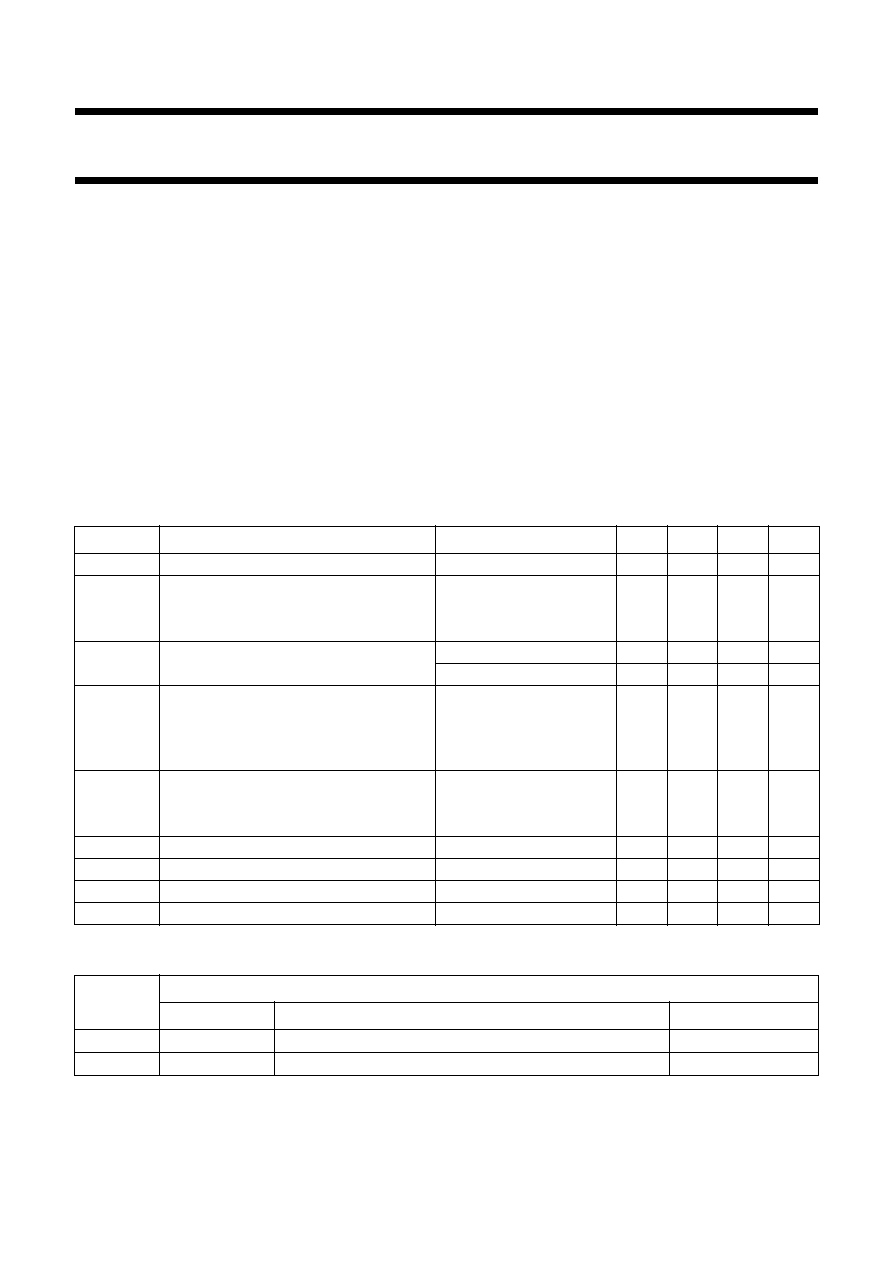
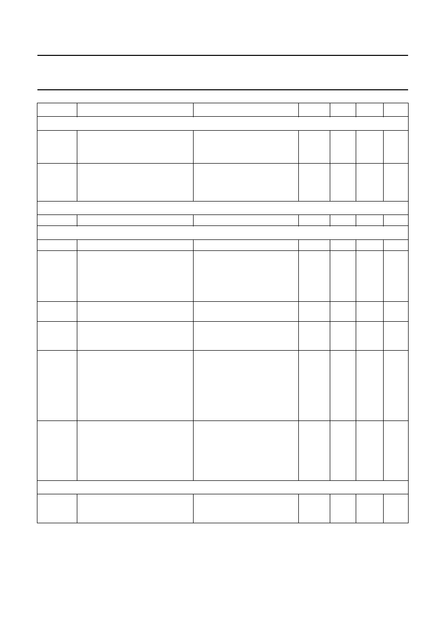
QUICK REFERENCE DATA
ORDERING INFORMATION
SYMBOL
PARAMETER
CONDITIONS
MIN.
TYP.
MAX.
UNIT
V
LN
line voltage
I
line
= 15 mA
4.2
4.45
4.7
V
I
line
line current
TEA1068
normal operation
10
-
140
mA
TEA1068T
normal operation
10
-
100
mA
I
CC
internal supply current
power down; input LOW
-
0.96
1.3
mA
power down; input HIGH
-
55
82
µ
A
V
CC
supply voltage for peripherals
I
line
= 15 mA;
MUTE = HIGH
I
p
= 1.2 mA
2.8
3.05
-
V
I
p
= 1.7 mA
2.5
-
-
V
G
v
voltage gain
microphone amplifier
44
-
60
dB
receiving amplifier
17
-
39
dB
G
v
line loss compensation gain control range
5.5
5.9
6.3
dB
V
exch
exchange supply voltage
24
-
60
V
R
exch
exchange feeding bridge resistance range
0.4
-
1
k
T
amb
ambient operating temperature
-
25
+75
∞
C
TYPE
NUMBER
PACKAGE
NAME
DESCRIPTION
VERSION
TEA1068
DIP18
plastic dual in-line package; 18 leads (300 mil)
SOT102-1
TEA1068T
SO20
plastic small outline package; 20 leads; body width 7.5 mm
SOT163-1
1996 Apr 23
3
Philips Semiconductors
Product specification
Versatile telephone transmission circuit
with dialler interface
TEA1068
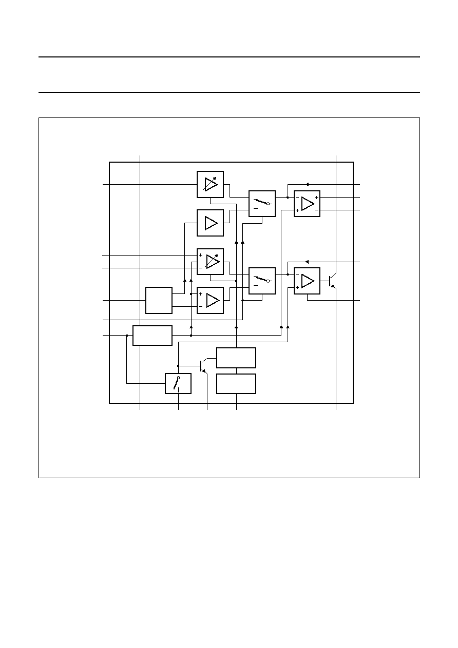
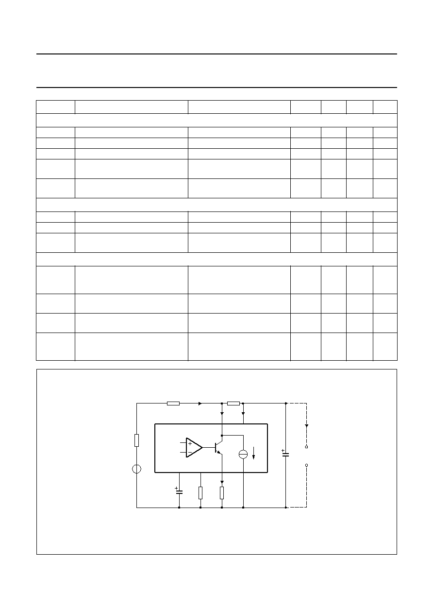
BLOCK DIAGRAM
Fig.1 Block diagram.
The figures in parentheses refer to the TEA1068T.
handbook, full pagewidth
MBH130
dB
SUPPLY AND
REFERENCE
AGC
CIRCUIT
SLPE
STAB
AGC
REG
VEE
CURRENT
REFERENCE
12 (14)
16 (18)
17 (19)
10 (11)
14 (16)
13 (15)
7 (7)
8 (9)
11 (12)
15 (17)
1 (1)
6 (6)
5 (5)
4 (4)
9 (10)
18 (20)
IR
MIC
+
MIC
-
DTMF
MUTE
PD
VCC
TEA1068
TEA1068T
LN
GAR
2 (2)
GAS1
3 (3)
GAS2
QR
+
QR
-

1996 Apr 23
4
Philips Semiconductors
Product specification
Versatile telephone transmission circuit
with dialler interface
TEA1068
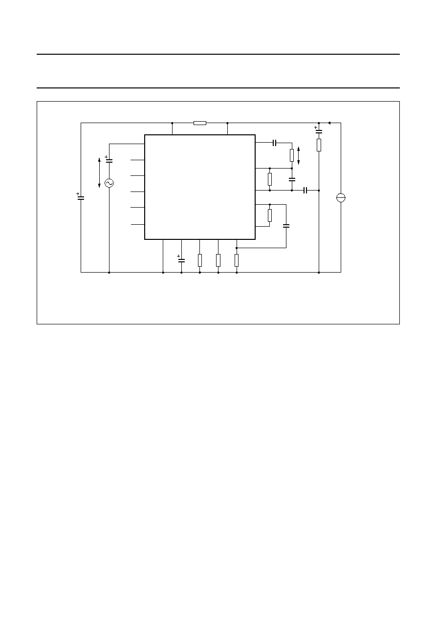
PINNING
SYMBOL
PIN
DESCRIPTION
TEA1068
TEA1068T
LN
1
1
positive line terminal
GAS1
2
2
gain adjustment transmitting amplifier
GAS2
3
3
gain adjustment transmitting amplifier
QR
-
4
4
inverting output receiving amplifier
QR+
5
5
non-inverting output receiving amplifier
GAR
6
6
gain adjustment receiving amplifier
MIC
-
7
7
inverting microphone input
n.c.
-
8
not connected
MIC+
8
9
non-inverting microphone input
STAB
9
10
current stabilizer
V
EE
10
11
negative line terminal
IR
11
12
receiving amplifier input
n.c.
-
13
not connected
PD
12
14
power-down input
DTMF
13
15
dual-tone multi-frequency input
MUTE
14
16
mute input
V
CC
15
17
positive supply decoupling
REG
16
18
voltage regulator decoupling
AGC
17
19
automatic gain control input
SLPE
18
20
slope (DC resistance) adjustment
Fig.2 Pin configuration TEA1068.
handbook, halfpage
1
2
3
4
5
6
7
8
9
18
17
16
15
14
13
12
11
10
MBH132
TEA1068
LN
GAS1
GAS2
QR
-
QR
+
GAR
MIC
-
MIC
+
SLPE
AGC
REG
VCC
DTMF
VEE
MUTE
PD
IR
STAB
handbook, halfpage
1
2
3
4
5
6
7
8
9
10
20
19
18
17
16
15
14
13
12
11
MBH131
TEA1068T
LN
GAS1
GAS2
QR
-
QR
+
GAR
MIC
-
n.c.
MIC
+
SLPE
AGC
REG
VCC
n.c.
DTMF
VEE
MUTE
PD
IR
STAB
Fig.3 Pin configuration TEA1068T.
1996 Apr 23
5
Philips Semiconductors
Product specification
Versatile telephone transmission circuit
with dialler interface
TEA1068
FUNCTIONAL DESCRIPTION
Supplies: V
CC
, LN, SLPE, REG and STAB
Power for the TEA1068 and its peripheral circuits is usually
obtained from the telephone line. The TEA1068 develops
its own supply at V
CC
and regulates its voltage drop. The
supply voltage VCC may also be used to supply external
circuits, e.g. dialling and control circuits.
Decoupling of the supply voltage is performed by a
capacitor between V
CC
and VEE; the internal voltage
regulator is decoupled by a capacitor between REG and
VEE.
The DC current flowing into the set is determined by the
exchange voltage (Vexch
), the feeding bridge resistance,
(R
exch
) and the DC resistance of the telephone line (R
line
).
An internal current stabilizer is set by a resistor of 3.6 k
between the current stabilizer pin STAB and V
EE
(see Fig.9).
If the line current I
line
exceeds the current ICC+ 0.5 mA
required by the circuit itself (approximately 1 mA) plus the
current I
p
required by the peripheral circuits connected to
V
CC
, then the voltage regulator diverts the excess current
via LN.
The regulated voltage on the line terminal (VLN) can be
calculated as:
V
LN
= V
ref
+ I SLPE
◊
R9
or
VLN= V
ref
+ [(Iline
-
I
CC
-
0.5
◊
10
3
)
-
Ip]
◊
R9
where V
ref
is an internally generated temperature
compensated reference voltage of 4.2 V and R9 is an
external resistor connected between SLPE and V
EE
.
The preferred value for R9 is 20
. Changing the value of
R9 will also affect microphone gain, DTMF gain, gain
control characteristics, side-tone level, the maximum
output swing on LN and the DC characteristics (especially
at lower voltages).
Under normal conditions, when I
SLPE
>> I
CC
+ 0.5 mA + Ip,
the static behaviour of the circuit is that of a 4.2 V regulator
diode with an internal resistance equal to that of R9. In the
audio frequency range, the dynamic impedance is largely
determined by R1 (see Fig.4).
The internal reference voltage can be adjusted by means
of an external resistor (R
VA
). This resistor, connected
between LN and REG, will decrease the internal reference
voltage; when connected between REG and SLPE, it will
increase the internal reference voltage. Current (Ip)
available from V
CC
for supplying peripheral circuits
depends on external components and on the line current.
Figure 10 shows this current for V
CC
> 2.2 V and for
VCC> 3 V, this being the minimum supply voltage for most
CMOS circuits, including voltage drop for an enable diode.
If MUTE is LOW, the available current is further reduced
when the receiving amplifier is driven.
Microphone inputs MIC+ and MIC
-
and gain
adjustment pins GAS1 and GAS2
The TEA1068 has symmetrical microphone inputs.
Its input impedance is 64 k
(2
◊
32 k
) and its voltage
gain is typically 52 dB (when R7
=
68 k
; see Fig.14).
Dynamic, magnetic, piezoelectric or electret (with built-in
FET source followers) microphones can be used.
The arrangements with the microphone types mentioned
are shown in Fig.11.
The gain of the microphone amplifier can be adjusted
between 44 dB and 60 dB. The gain is proportional to the
value of the external resistor R7 connected between GAS1
and GAS2. An external capacitor C6 of 100 pF between
GAS1 and SLPE is required to ensure stability. A larger
value may be chosen to obtain a first-order low-pass filter.
The cut-off frequency corresponds with the time constant
R7
◊
C6.
Fig.4 Equivalent impedance circuit.
R
p
=
17.5 k
L
eq
=
C3
◊
R9
◊
R
p
handbook, halfpage
MBA454
R9
20
REG
LN
C3
4.7
µ
F
Rp
Vref
Leq
VCC
VEE
C1
100
µ
F
R1

1996 Apr 23
6
Philips Semiconductors
Product specification
Versatile telephone transmission circuit
with dialler interface
TEA1068
Mute input (MUTE)
A HIGH level at MUTE enables the DTMF input and
inhibits the microphone and the receiving amplifier inputs.
A LOW level or an open circuit has the reverse effect.
MUTE switching causes only negligible clicks at the
earpiece outputs and on the line.
Dual-Tone Multi Frequency input (DTMF)
When the DTMF input is enabled, dialling tones may be
sent onto the line. The voltage gain from DTMF to LN is
typically 25.5 dB (when R7
=
68 k
) and varies with R7 in
the same way as the gain of the microphone amplifier.
The signalling tones can be heard in the telephone
earpiece at a low level (confidence tone).
Receiving amplifier: IR, QR+, QR
-
and GAR
The receiving amplifier has one input IR and two
complementary outputs, a non-inverting output QR+ and
an inverting output QR
-
. These outputs may be used for
single-ended or for differential drive depending on the
sensitivity and type of earpiece used (see Fig.12). Gain
from IR to QR+ is typically 25 dB (when R4 = 100 k
).
This is sufficient for low-impedance magnetic or dynamic
microphones, which are suited for single-ended drive.
By using both outputs (differential drive), the gain is
increased by 6 dB. This feature can be used when the
earpiece impedance exceeds 450
, (high-impedance
dynamic or piezoelectric types).
The output voltage of the receiving amplifier is specified for
continuous-wave drive. The maximum output voltage will
be higher under speech conditions where the ratio of peak
to RMS value is higher.
The receiving amplifier gain can be adjusted between
17 dB and 33 dB with single-ended drive and between
26 dB and 39 dB with differential drive to suit the sensitivity
of the transducer used. The gain is set by the external
resistor R4 connected between GAR and QR+. Overall
receive gain between LN and QR+ is calculated by
subtracting the anti-side-tone network attenuation (32 dB)
from the amplifier gain. Two external capacitors,
C4 = 100 pF and C7 = 10
◊
C4 = 1 nF, are necessary to
ensure stability. A larger value of C4 may be chosen to
obtain a first-order, low-pass filter. The `cut-off' frequency
corresponds with the time constant R4
◊
C4.
Automatic Gain Control input AGC
Automatic line loss compensation is achieved by
connecting a resistor R6 between AGC and V
EE
. This
automatic gain control varies the microphone amplifier
gain and the receiving amplifier gain in accordance with
the DC line current.
The control range is 5.9 dB. This corresponds to a line
length of 5 km for a 0.5 mm diameter copper twisted-pair
cable with a DC resistance of 176
/km and an average
attenuation 1.2 dB/km.
Resistor R6 should be chosen in accordance with the
exchange supply voltage and its feeding bridge resistance
(see Fig.13 and Table 1). Different values of R6 give the
same ratio of line currents for start and end of the control
range. If automatic line loss compensation is not required,
AGC may be left open. The amplifiers then all give their
maximum gain as specified.
Power-Down input (PD)
During pulse dialling or register recall (timed loop break),
the telephone line is interrupted. During these
interruptions, the telephone line provides no power for the
transmission circuit or circuits supplied by V
CC
. The charge
held on C1 will bridge these gaps. This bridging is made
easier by a HIGH level on the PD input, which reduces the
typical supply current from 1 mA to 55
µ
A and switches off
the voltage regulator, thus preventing discharge through
LN. When PD is HIGH, the capacitor at REG is
disconnected with the effect that the voltage stabilizer will
have no switch-on delay after line interruptions. This
minimizes the contribution of the IC to the current
waveform during pulse dialling or register recall. When this
facility is not required, PD may be left open-circuit.
Side-tone suppression
Suppression of the transmitted signal in the earpiece is
obtained by the anti-side-tone network consisting of
R1//Z
line
, R2, R3 and Z
bal
(see Fig.14). Maximum
compensation is obtained when the following conditions
are fulfilled:
(1)
(2)
R9
R2
◊
R1 R3
R8//Z
bal
[
]
+
(
)
=
Z
bal
Z
bal
R8
+
(
)
/
Z
line
Z
line
R1
+
(
)
/
=
[
]

1996 Apr 23
7
Philips Semiconductors
Product specification
Versatile telephone transmission circuit
with dialler interface
TEA1068
If fixed values are chosen for R1, R2, R3 and R9, then
condition (1) will always be fulfilled, provided that
R8//Z
bal
<< R3. To obtain optimum side-tone
suppression, condition (2) has to be fulfilled, resulting in:
Z
bal
=
(R8/R1) Z
line
=
k
◊
Z
line
, where k is a scale factor:
k
=
(R8/R1).
Scale factor k (dependent on the value of R8) must be
chosen to meet the following criteria:
1. Compatibility with a standard capacitor from the E6 or
E12 range for Z
bal
2.
Z
bal
//R8
<< R3 to fulfil condition (1) and thus
ensuring correct anti-side-tone bridge operation
3.
Z
bal
+ R8
>> R9 to avoid influencing the transmitter
gain.
In practice, Z
line
varies greatly with the line length and
cable type; consequently, an average value has to be
chosen for Z
bal
, thus giving an optimum setting for short or
long lines.
Example: the balanced line impedance (Z
bal
) at which the
optimum suppression is preset can be calculated by:
Assume Z
line
= 210
+ (1265
/140 nF), representing a
5 km line of 0.5 mm diameter, copper, twisted-pair cable
matched to 600
(176
/km; 38 nF/km). When k = 0.64,
then R8 = 390
; Z
bal
= 130
+ (820
//220 nF).
The anti-side-tone network for the TEA1060 family shown
in Fig.5 attenuates the signal received from the line by
32 dB before it enters the receiving amplifier.
The attenuation is almost constant over the whole audio
frequency range.
Figure 6 shows a conventional Wheatstone bridge
anti-side-tone circuit that can be used as an alternative.
Both bridge types can be used with either resistive or
complex set impedances.
Fig.5 Equivalent circuit of TEA1060 family anti-side-tone bridge.
handbook, full pagewidth
MSA500
R1
R2
R9
R3
IR
R8
VEE
SLPE
LN
Zline
Rt
im
Zbal

1996 Apr 23
8
Philips Semiconductors
Product specification
Versatile telephone transmission circuit
with dialler interface
TEA1068
LIMITING VALUES
In accordance with the Absolute Maximum Rating System (IEC 134).
Notes
1. Mostly dependent on the maximum required T
amb
and on the voltage between LN and SLPE. See Figs 7 and 8 to
determine the current as a function of the required voltage and the temperature.
2. Calculated for the maximum ambient temperature specified T
amb
= 75
∞
C and a maximum junction temperature of
125
∞
C.
SYMBOL
PARAMETER
CONDITIONS
MIN.
MAX.
UNIT
V
LN
positive continuous line voltage
-
12
V
V
LN(R)
repetitive line voltage during switch-on or
line interruption
-
13.2
V
V
LN(RM)
repetitive peak line voltage for a 1 ms pulse
per 5 s
R9 = 20
;
R10 = 13
; (
Fig.15)
-
28
V
I
line
line current
R9 = 20
; note 1
-
140
mA
V
n
voltage on any other pin
V
EE
-
0.7
V
CC
+ 0.7
V
P
tot
total power dissipation
R9 = 20
; note 2
TEA1068
-
769
mW
TEA1068T
-
555
mW
T
stg
IC storage temperature
-
40
+125
∞
C
T
amb
operating ambient temperature
-
25
+75
∞
C
T
j
junction temperature
-
125
∞
C
Fig.6 Equivalent circuit of an anti-side-tone network in a Wheatstone bridge configuration.
ndbook, full pagewidth
MSA501
R1
R9
IR
R8
VEE
SLPE
LN
Zline
Rt
im
RA
Zbal

1996 Apr 23
9
Philips Semiconductors
Product specification
Versatile telephone transmission circuit
with dialler interface
TEA1068
THERMAL CHARACTERISTICS
SYMBOL
PARAMETER
VALUE
UNIT
R
th j-a
thermal resistance from junction to ambient in free air
TEA1068
65
K/W
TEA1068T
90
K/W
Fig.7 Safe operating area TEA1068.
handbook, halfpage
2
12
160
40
80
120
60
100
140
MBH133
4
6
8
10
VLN-VSLPE (V)
ILN
(mA)
(1)
(2)
(3)
(4)
(1) T
amb
= 45
∞
C; P
tot
= 1231 mW.
(2) T
amb
= 55
∞
C; P
tot
= 1077 mW.
(3) T
amb
= 65
∞
C; P
tot
= 923 mW.
(4) T
amb
= 75
∞
C; P
tot
= 769 mW.
Fig.8 Safe operating area TEA1068T.
handbook, halfpage
2
12
150
30
70
110
MBH125
4
6
8
10
130
90
50
ILN
(mA)
(1)
(2)
(3)
(4)
VLN
-
VSLPE (V)
(1) T
amb
= 45
∞
C; P
tot
= 888 mW.
(2) T
amb
= 55
∞
C; P
tot
= 777 mW.
(3) T
amb
= 65
∞
C; P
tot
= 666 mW.
(4) T
amb
= 75
∞
C; P
tot
= 555 mW.
1996 Apr 23
10
Philips Semiconductors
Product specification
Versatile telephone transmission circuit
with dialler interface
TEA1068
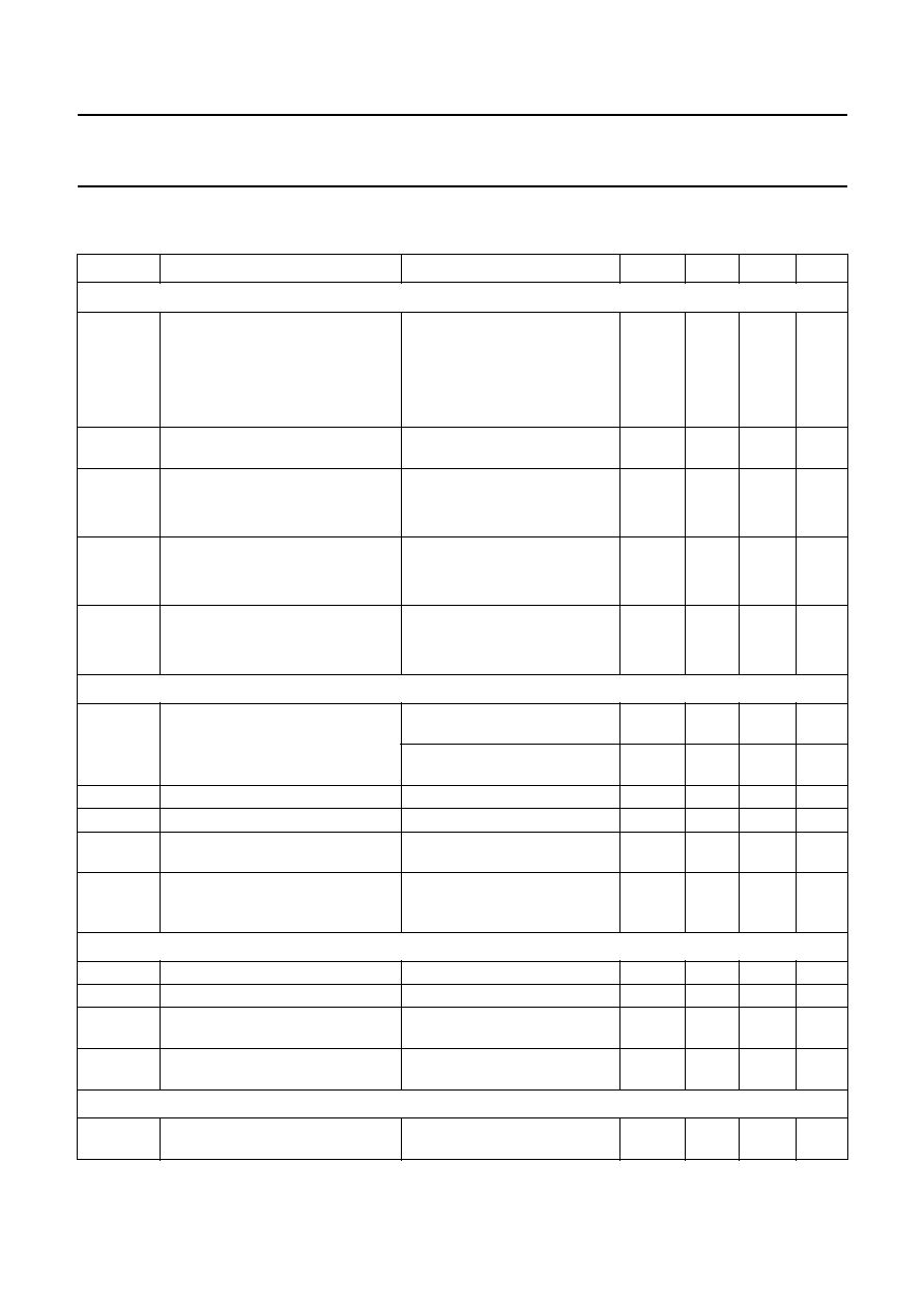
CHARACTERISTICS
I
line
= 10 to 140 mA; V
EE
= 0 V; f = 800 Hz; T
amb
= 25
∞
C; unless otherwise specified.
SYMBOL
PARAMETER
CONDITIONS
MIN.
TYP.
MAX.
UNIT
Supplies: LN and V
CC
V
LN
voltage drop over circuit between
LN and V
EE
microphone inputs open
I
line
= 5 mA
3.95
4.25
4.55
V
I
line
= 15 mA
4.2
4.45
4.7
V
I
line
= 100 mA
5.4
6.1
6.7
V
I
line
= 140 mA
-
-
7.5
V
V
LN
/
T
voltage drop variation with
temperature
I
line
= 15 mA
-
4
-
2
0
mV/K
V
LN
voltage drop over circuit, between
LN and V
EE
with external resistor
R
VA
I
line
= 15 mA
R
VA
(LN to REG) = 68 k
3.45
3.8
4.1
V
R
VA
(REG to SLPE) = 39 k
4.65
5
5.35
V
I
CC
supply current
V
CC
= 2.8 V
PD = LOW
-
0.96
1.3
mA
PD = HIGH
-
55
82
µ
A
V
CC
supply voltage available for
peripheral circuitry
I
line
= 15 mA; MUTE = HIGH
I
p
= 1.2 mA
2.8
3.05
-
V
I
p
= 0 mA
3.5
3.75
-
V
Microphone inputs MIC+ and MIC
-
Z
i
input impedance
differential between
MIC+ and MIC
-
51
64
77
k
single-ended MIC+ or
MIC
-
to V
EE
25.5
32
38.5
k
CMRR
common mode rejection ratio
-
82
-
dB
G
v
voltage gain from MIC+/MIC
-
to LN I
line
= 15 mA; R7 = 68 k
;
51
52
53
dB
G
vf
gain variation with frequency at
f = 300 Hz and f = 3400 Hz
with respect to 800 Hz
-
0.5
±
0.2
+0.5
dB
G
vT
gain variation with temperature at
-
25
∞
C and +75
∞
C
I
line
= 50 mA;
with respect to 25
∞
C; without
R6
-
±
0.2
-
dB
Dual-tone multi-frequency input DTMF
Z
i
input impedance
16.8
20.7
24.6
k
G
v
voltage gain from DTMF to LN
I
line
= 15 mA; R7 = 68 k
24.5
25.5
26.5
dB
G
vf
gain variation with frequency at
f = 300 Hz and f = 3400 Hz
with respect to 800 Hz
-
0.5
±
0.2
+0.5
dB
G
vT
gain variation with temperature at
T
amb
= -
25
∞
C and +75
∞
C
I
line
= 50 mA;
with respect to 25
∞
C
-
±
0.5
-
dB
Gain adjustment connections GAS1 and GAS2
G
v
gain variation with R7, transmitting
amplifier
-
8
-
+8
dB
1996 Apr 23
11
Philips Semiconductors
Product specification
Versatile telephone transmission circuit
with dialler interface
TEA1068
Transmitting amplifier output LN
V
LN(rms)
output voltage (RMS value)
I
line
= 15 mA
THD = 2%
1.9
2.3
-
V
THD = 10%
-
2.6
-
V
V
no(rms)
noise output voltage (RMS value)
I
line
= 15 mA; R7 = 68 k
;
200
between MIC
-
and
MIC+; psophometrically
weighted (P53 curve)
-
-
72
-
dBmp
Receiving amplifier input IR
Z
i
input impedance
17
21
25
k
Receiving amplifier outputs QR+ and QR
-
Z
o
output impedance
single ended
-
4
-
G
v
voltage gain from IR to QR+ or
QR
-
I
line
= 15 mA
R
L
(from QR+ or
QR
-
) = 300
; single-ended
24
25
26
dB
R
L
(from QR+ or
QR
-
) = 600
; differential
30
31
32
dB
G
vf
gain variation with frequency at
f = 300 Hz and f = 3400 Hz
with respect to 800 Hz
-
0.5
-
0.2
0
dB
G
vT
gain variation with temperature at
T
amb
= -
25
∞
C and +75
∞
C
I
line
= 50 mA;
with respect to 25
∞
C;
without R6
-
±
0.2
-
dB
V
o(rms)
output voltage (RMS value)
sine wave drive; I
line
= 15 mA;
I
p
= 0 mA; THD = 2%;
R4 = 100 k
single-ended; R
L
= 150
0.3
0.38
-
V
single-ended; R
L
= 450
0.4
0.52
-
V
differential; f = 3400 Hz;
R
series
= 100
; C
L
= 47 nF
0.8
1.0
-
V
V
no(rms)
noise output voltage (RMS value)
I
line
= 15 mA; R4 = 100 k
;
IR open-circuit
psophometrically weighted
(P53 curve)
single-ended; R
L
= 300
-
50
-
µ
V
differential; R
L
= 600
-
100
-
µ
V
Gain adjustment GAR
G
v
gain variation of receiving amplifier
achievable by varying R4 between
GAR and QR
-
8
-
+8
dB
SYMBOL
PARAMETER
CONDITIONS
MIN.
TYP.
MAX.
UNIT
1996 Apr 23
12
Philips Semiconductors
Product specification
Versatile telephone transmission circuit
with dialler interface
TEA1068
MUTE input
V
IH
HIGH level input voltage
1.5
-
V
CC
V
V
IL
LOW level input voltage
-
-
0.3
V
I
MUTE
input current
-
8
15
µ
A
G
v
voltage gain reduction between
MIC+ and MIC
-
to LN
MUTE = HIGH
-
70
-
dB
G
v
voltage gain from DTMF to QR+ or
QR
-
MUTE = HIGH; R4 = 100 k
;
single-ended; R
L
= 300
-
21
-
19
-
17
dB
Power-Down input PD
V
IH
HIGH level input voltage
1.5
-
V
CC
V
V
IL
LOW level input voltage
-
-
0.3
V
I
pd
input current in power-down
condition
-
5
10
µ
A
Automatic Gain Control input AGC
G
v
gain control range from IR to
QR+/QR
-
and from MIC+/MIC
-
to
LN
I
line
= 70 mA; R6 = 110 k
between AGC and V
EE
-
5.5
-
5.9
-
6.3
dB
I
line(H)
highest line current for maximum
gain
R6 = 110 k
between AGC
and V
EE
-
23
-
mA
I
line(L)
lowest line current for minimum
gain
R6 = 110 k
between AGC
and V
EE
-
61
-
mA
G
v
voltage gain variation
between I
line
= 15 mA and
I
line
= 35 mA; R6 = 110 k
between AGC and V
EE
-
1.0
-
1.5
-
2.0
dB
SYMBOL
PARAMETER
CONDITIONS
MIN.
TYP.
MAX.
UNIT
andbook, full pagewidth
MBH134
SLPE
STAB
REG
VEE
VCC
Ip
LN
TEA1068
SLPE
I
AC
DC
peripheral
circuits
C1
0.5 mA
ISLPE
+
0.5 mA
Rline
Rexch
Vexch
Iline
R1
ICC
C3
R5
R9
Fig.9 Supply arrangement.

1996 Apr 23
13
Philips Semiconductors
Product specification
Versatile telephone transmission circuit
with dialler interface
TEA1068
Fig.10 Typical current I
p
available from V
CC
for peripheral circuitry with V
CC
2.2 V.
Curve (1) is valid when the receiving amplifier is not driven or when MUTE = HIGH. Curve (2) is valid when MUTE = LOW and the receiving amplifier
is driven; V
o(rms)
= 150 mV; R
L
= 150
asymmetrical.
The supply possibilities can be increased simply by setting the voltage drop over the circuit V
LN
to a higher value by means of resistor R
VA
connected
between REG and SLPE.
handbook, halfpage
0
1
(1)
(2)
(3)
(4)
Ip
(mA)
2
4
VCC (V)
3
0
1
2
MBH124
3
Fig.11 Alternative microphone arrangements.
handbook, full pagewidth
MBH135
VEE
VCC
MIC
+
MIC
-
(1)
MIC
-
MIC
+
MIC
-
MIC
+
(1) May be connected to decrease the terminating impedance.
a. Magnetic or dynamic
microphone.
b. Electret microphone.
c. Piezoelectric microphone.

1996 Apr 23
14
Philips Semiconductors
Product specification
Versatile telephone transmission circuit
with dialler interface
TEA1068
Fig.12 Alternative receiver arrangements.
(1) May be connected to prevent distortion (inductive load).
(2) Required to increase the phase margin (capacitive load).
a. Dynamic earpiece
with less than 450
impedance.
b. Dynamic earpiece with
more than 450
impedance.
c. Magnetic earpiece
with more than 450
impedance.
d. Piezoelectric
earpiece.
handbook, full pagewidth
(1)
MBH136
(2)
QR
+
QR
-
QR
+
QR
-
QR
+
QR
-
QR
+
VEE
QR
-
Fig.13 Variation of gain with line current, with R6 as a parameter.
dbook, full pagewidth
MBH137
-
6
-
4
-
2
0
140
120
100
80
60
40
20
0
78.7 k
48.7 k
110 k
140 k
R6
=
Iline(mA)
Gv
(dB)
R9 = 20
.

1996 Apr 23
15
Philips Semiconductors
Product specification
Versatile telephone transmission circuit
with dialler interface
TEA1068
Table 1
Values of resistor R6 for optimum line loss compensation, for various usual values of exchange supply
voltage V
exch
and exchange feeding bridge resistance R
exch
; R9 = 20
V
exch
(V)
R6 (k
)
R
exch
= 400
R
exch
= 600
R
exch
= 800
R
exch
= 1000
24
61.9
48.7
X
X
36
100
78.7
68
60.4
48
140
110
93.1
82
60
X
X
120
102
Fig.14 Test circuit for defining voltage gain of MIC+, MIC
-
and DTMF inputs.
Voltage gain is defined as; G
v
= 20 log
V
o
/V
i
. For measuring the gain from MIC+ and MIC
-
, the MUTE input should be LOW or open, for measuring
the DTMF input, MUTE should be HIGH. Inputs not under test should be open.
handbook, full pagewidth
Iline
MBH138
R6
R5
3.6
k
R9
20
SLPE
STAB
AGC
REG
VEE
GAS2
GAS1
R7
68 k
R4
100 k
C4
100 pF
C7 1 nF
C6
100 pF
100
µ
F
RL
600
Vo
VCC
LN
R1
620
10 to 140 mA
10
µ
F
Vi
C1
100
µ
F
Vi
IR
MIC
+
MIC
-
DTMF
MUTE
PD
TEA1068
QR
+
GAR
QR
-
C3
4.7
µ
F
1996 Apr 23
16
Philips Semiconductors
Product specification
Versatile telephone transmission circuit
with dialler interface
TEA1068
Fig.15 Test circuit for defining voltage gain of the receiving amplifier.
Voltage gain is defined as; G
v
= 20 log
V
o
/V
i
.
handbook, full pagewidth
MBH139
R6
R7
C6
100 pF
R1
I line
10 to 140 mA
C1
C4
100 pF
C7 1 nF
R5
3.6
k
R9
20
R4
100
k
100
µ
F
10
µ
F
600
620
10
µ
F
100
µ
F
C3
4.7
µ
F
SLPE
STAB
AGC
REG
VEE
GAS2
GAS1
VCC
LN
IR
MIC
+
MIC
-
DTMF
MUTE
PD
TEA1068
QR
+
GAR
QR
-
ZL
Vo
Vi

1996 Apr 23
17
Philips Semiconductors
Product specification
Versatile telephone transmission circuit
with dialler interface
TEA1068
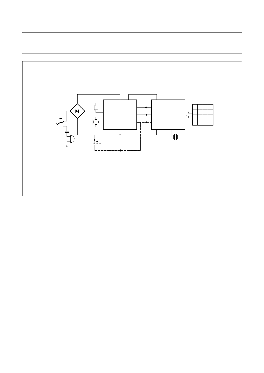
APPLICATION INFORMATION
Fig.16 Application diagram.
Typical application of the TEA1068, shown here with a piezoelectric earpiece and DTMF dialling. The bridge to the left and R10 limit the current into
the circuit and the voltage across the circuit during line transients. Pulse dialling or register recall require a different protection arrangement.
handbook, full pagewidth
MBH140
SLPE
GAS1 GAS2
C6
100 pF
R8
390
MIC
-
MIC
+
GAR
QR
+
QR
-
C4
100 pF
C5
100 nF
IR
REG
R7
AGC
R6
STAB
VEE
C3
4.7
µ
F
R5
3.6 k
R1
LN
VCC
620
R9
20
PD
DTMF
MUTE
1 nF
C7
R4
BZW14
(2x)
BAS11
(2x)
R11
R3
3.92
k
R3
130 k
R10
13
Zbal
TEA1068
C1
100
µ
F
from dial
and
control
circuits
telephone
line
1996 Apr 23
18
Philips Semiconductors
Product specification
Versatile telephone transmission circuit
with dialler interface
TEA1068
Fig.17 DTMF set with a CMOS DTMF dialling circuit.
handbook, full pagewidth
MBA279 - 1
telephone
line
cradle
contact
TEA1068
LN
VCC
DTMF
TONE
MUTE
PD
DP/FLO
VEE
VSS
VDD
M1
PCD3310
BSN254A
The dashed lines show an optional flash (register recall by timed loop break).

1996 Apr 23
19
Philips Semiconductors
Product specification
Versatile telephone transmission circuit
with dialler interface
TEA1068
PACKAGE OUTLINES
REFERENCES
OUTLINE
VERSION
EUROPEAN
PROJECTION
ISSUE DATE
IEC
JEDEC
EIAJ
SOT102-1
93-10-14
95-01-23
UNIT
A
max.
1
2
b
1
(1)
(1)
(1)
b
2
c
D
E
e
M
Z
H
L
mm
DIMENSIONS (inch dimensions are derived from the original mm dimensions)
A
min.
A
max.
b
max.
w
M
E
e
1
1.40
1.14
0.53
0.38
0.32
0.23
21.8
21.4
6.48
6.20
3.9
3.4
0.254
2.54
7.62
8.25
7.80
9.5
8.3
0.85
4.7
0.51
3.7
inches
0.055
0.044
0.021
0.015
0.013
0.009
1.40
1.14
0.055
0.044
0.86
0.84
0.26
0.24
0.15
0.13
0.01
0.10
0.30
0.32
0.31
0.37
0.33
0.033
0.19
0.020
0.15
M
H
c
(e )
1
M
E
A
L
seating plane
A
1
w
M
b
1
b
2
e
D
A
2
Z
18
1
10
9
b
E
pin 1 index
0
5
10 mm
scale
Note
1. Plastic or metal protrusions of 0.25 mm maximum per side are not included.
DIP18: plastic dual in-line package; 18 leads (300 mil)
SOT102-1

1996 Apr 23
20
Philips Semiconductors
Product specification
Versatile telephone transmission circuit
with dialler interface
TEA1068
UNIT
A
max.
A
1
A
2
A
3
b
p
c
D
(1)
E
(1)
(1)
e
H
E
L
L
p
Q
Z
y
w
v
REFERENCES
OUTLINE
VERSION
EUROPEAN
PROJECTION
ISSUE DATE
IEC
JEDEC
EIAJ
mm
inches
2.65
0.30
0.10
2.45
2.25
0.49
0.36
0.32
0.23
13.0
12.6
7.6
7.4
1.27
10.65
10.00
1.1
1.0
0.9
0.4
8
0
o
o
0.25
0.1
DIMENSIONS (inch dimensions are derived from the original mm dimensions)
Note
1. Plastic or metal protrusions of 0.15 mm maximum per side are not included.
1.1
0.4
SOT163-1
10
20
w
M
b
p
detail X
Z
e
11
1
D
y
0.25
075E04
MS-013AC
pin 1 index
0.10
0.012
0.004
0.096
0.089
0.019
0.014
0.013
0.009
0.51
0.49
0.30
0.29
0.050
1.4
0.055
0.419
0.394
0.043
0.039
0.035
0.016
0.01
0.25
0.01
0.004
0.043
0.016
0.01
0
5
10 mm
scale
X
A
A
1
A
2
H
E
L
p
Q
E
c
L
v
M
A
(A )
3
A
SO20: plastic small outline package; 20 leads; body width 7.5 mm
SOT163-1
95-01-24
97-05-22

1996 Apr 23
21
Philips Semiconductors
Product specification
Versatile telephone transmission circuit
with dialler interface
TEA1068
SOLDERING
Introduction
There is no soldering method that is ideal for all IC
packages. Wave soldering is often preferred when
through-hole and surface mounted components are mixed
on one printed-circuit board. However, wave soldering is
not always suitable for surface mounted ICs, or for
printed-circuits with high population densities. In these
situations reflow soldering is often used.
This text gives a very brief insight to a complex technology.
A more in-depth account of soldering ICs can be found in
our
"IC Package Databook" (order code 9398 652 90011).
DIP
S
OLDERING BY DIPPING OR BY WAVE
The maximum permissible temperature of the solder is
260
∞
C; solder at this temperature must not be in contact
with the joint for more than 5 seconds. The total contact
time of successive solder waves must not exceed
5 seconds.
The device may be mounted up to the seating plane, but
the temperature of the plastic body must not exceed the
specified maximum storage temperature (T
stg max
). If the
printed-circuit board has been pre-heated, forced cooling
may be necessary immediately after soldering to keep the
temperature within the permissible limit.
R
EPAIRING SOLDERED JOINTS
Apply a low voltage soldering iron (less than 24 V) to the
lead(s) of the package, below the seating plane or not
more than 2 mm above it. If the temperature of the
soldering iron bit is less than 300
∞
C it may remain in
contact for up to 10 seconds. If the bit temperature is
between 300 and 400
∞
C, contact may be up to 5 seconds.
SO
R
EFLOW SOLDERING
Reflow soldering techniques are suitable for all SO
packages.
Reflow soldering requires solder paste (a suspension of
fine solder particles, flux and binding agent) to be applied
to the printed-circuit board by screen printing, stencilling or
pressure-syringe dispensing before package placement.
Several techniques exist for reflowing; for example,
thermal conduction by heated belt. Dwell times vary
between 50 and 300 seconds depending on heating
method. Typical reflow temperatures range from
215 to 250
∞
C.
Preheating is necessary to dry the paste and evaporate
the binding agent. Preheating duration: 45 minutes at
45
∞
C.
W
AVE SOLDERING
Wave soldering techniques can be used for all SO
packages if the following conditions are observed:
∑
A double-wave (a turbulent wave with high upward
pressure followed by a smooth laminar wave) soldering
technique should be used.
∑
The longitudinal axis of the package footprint must be
parallel to the solder flow.
∑
The package footprint must incorporate solder thieves at
the downstream end.
During placement and before soldering, the package must
be fixed with a droplet of adhesive. The adhesive can be
applied by screen printing, pin transfer or syringe
dispensing. The package can be soldered after the
adhesive is cured.
Maximum permissible solder temperature is 260
∞
C, and
maximum duration of package immersion in solder is
10 seconds, if cooled to less than 150
∞
C within
6 seconds. Typical dwell time is 4 seconds at 250
∞
C.
A mildly-activated flux will eliminate the need for removal
of corrosive residues in most applications.
R
EPAIRING SOLDERED JOINTS
Fix the component by first soldering two diagonally-
opposite end leads. Use only a low voltage soldering iron
(less than 24 V) applied to the flat part of the lead. Contact
time must be limited to 10 seconds at up to 300
∞
C. When
using a dedicated tool, all other leads can be soldered in
one operation within 2 to 5 seconds between
270 and 320
∞
C.

1996 Apr 23
22
Philips Semiconductors
Product specification
Versatile telephone transmission circuit
with dialler interface
TEA1068
DEFINITIONS
LIFE SUPPORT APPLICATIONS
These products are not designed for use in life support appliances, devices, or systems where malfunction of these
products can reasonably be expected to result in personal injury. Philips customers using or selling these products for
use in such applications do so at their own risk and agree to fully indemnify Philips for any damages resulting from such
improper use or sale.
Data sheet status
Objective specification
This data sheet contains target or goal specifications for product development.
Preliminary specification
This data sheet contains preliminary data; supplementary data may be published later.
Product specification
This data sheet contains final product specifications.
Limiting values
Limiting values given are in accordance with the Absolute Maximum Rating System (IEC 134). Stress above one or
more of the limiting values may cause permanent damage to the device. These are stress ratings only and operation
of the device at these or at any other conditions above those given in the Characteristics sections of the specification
is not implied. Exposure to limiting values for extended periods may affect device reliability.
Application information
Where application information is given, it is advisory and does not form part of the specification.

1996 Apr 23
23
Philips Semiconductors
Product specification
Versatile telephone transmission circuit
with dialler interface
TEA1068
NOTES

Philips Semiconductors ≠ a worldwide company
Argentina: see South America
Australia: 34 Waterloo Road, NORTH RYDE, NSW 2113,
Tel. (02) 805 4455, Fax. (02) 805 4466
Austria: Computerstr. 6, A-1101 WIEN, P.O. Box 213,
Tel. (01) 60 101-1256, Fax. (01) 60 101-1250
Belarus: Hotel Minsk Business Center, Bld. 3, r. 1211,
Volodarski Str. 6, 220050 MINSK,
Tel. (172) 200 733, Fax. (172) 200 773
Belgium: see The Netherlands
Brazil: see South America
Bulgaria: Philips Bulgaria Ltd., Energoproject, 15th floor,
51 James Bourchier Blvd., 1407 SOFIA,
Tel. (359) 2 689 211, Fax. (359) 2 689 102
Canada: PHILIPS SEMICONDUCTORS/COMPONENTS:
Tel. (800) 234-7381, Fax. (708) 296-8556
Chile: see South America
China/Hong Kong: 501 Hong Kong Industrial Technology Centre,
72 Tat Chee Avenue, Kowloon Tong, HONG KONG,
Tel. (852) 2319 7888, Fax. (852) 2319 7700
Colombia: see South America
Czech Republic: see Austria
Denmark: Prags Boulevard 80, PB 1919, DK-2300
COPENHAGEN S, Tel. (032) 88 2636, Fax. (031) 57 1949
Finland: Sinikalliontie 3, FIN-02630 ESPOO,
Tel. (358) 0-615 800, Fax. (358) 0-61580 920
France: 4 Rue du Port-aux-Vins, BP317,
92156 SURESNES Cedex,
Tel. (01) 4099 6161, Fax. (01) 4099 6427
Germany: P.O. Box 10 51 40, 20035 HAMBURG,
Tel. (040) 23 53 60, Fax. (040) 23 53 63 00
Greece: No. 15, 25th March Street, GR 17778 TAVROS,
Tel. (01) 4894 339/4894 911, Fax. (01) 4814 240
Hungary: see Austria
India: Philips INDIA Ltd, Shivsagar Estate, A Block,
Dr. Annie Besant Rd. Worli, BOMBAY 400 018
Tel. (022) 4938 541, Fax. (022) 4938 722
Indonesia: see Singapore
Ireland: Newstead, Clonskeagh, DUBLIN 14,
Tel. (01) 7640 000, Fax. (01) 7640 200
Israel: RAPAC Electronics, 7 Kehilat Saloniki St, TEL AVIV 61180,
Tel. (03) 645 04 44, Fax. (03) 648 10 07
Italy: PHILIPS SEMICONDUCTORS,
Piazza IV Novembre 3, 20124 MILANO,
Tel. (0039) 2 6752 2531, Fax. (0039) 2 6752 2557
Japan: Philips Bldg 13-37, Kohnan 2-chome, Minato-ku,
TOKYO 108, Tel. (03) 3740 5130, Fax. (03) 3740 5077
Korea: Philips House, 260-199 Itaewon-dong,
Yongsan-ku, SEOUL, Tel. (02) 709-1412, Fax. (02) 709-1415
Malaysia: No. 76 Jalan Universiti, 46200 PETALING JAYA,
SELANGOR, Tel. (03) 750 5214, Fax. (03) 757 4880
Mexico: 5900 Gateway East, Suite 200, EL PASO,
TEXAS 79905, Tel. 9-5(800) 234-7831, Fax. (708) 296-8556
Middle East: see Italy
Netherlands: Postbus 90050, 5600 PB EINDHOVEN, Bldg. VB,
Tel. (040) 2783749, Fax. (040) 2788399
New Zealand: 2 Wagener Place, C.P.O. Box 1041, AUCKLAND,
Tel. (09) 849-4160, Fax. (09) 849-7811
Norway: Box 1, Manglerud 0612, OSLO,
Tel. (022) 74 8000, Fax. (022) 74 8341
Philippines: PHILIPS SEMICONDUCTORS PHILIPPINES Inc.,
106 Valero St. Salcedo Village, P.O. Box 2108 MCC,
MAKATI, Metro MANILA,
Tel. (63) 2 816 6380, Fax. (63) 2 817 3474
Poland: Ul. Lukiska 10, PL 04-123 WARSZAWA,
Tel. (022) 612 2831, Fax. (022) 612 2327
Portugal: see Spain
Romania: see Italy
Singapore: Lorong 1, Toa Payoh, SINGAPORE 1231,
Tel. (65) 350 2000, Fax. (65) 251 6500
Slovakia: see Austria
Slovenia: see Italy
South Africa: S.A. PHILIPS Pty Ltd.,
195-215 Main Road Martindale, 2092 JOHANNESBURG,
P.O. Box 7430 Johannesburg 2000,
Tel. (011) 470-5911, Fax. (011) 470-5494
South America: Rua do Rocio 220 - 5th floor, Suite 51,
CEP: 04552-903-S√O PAULO-SP, Brazil,
P.O. Box 7383 (01064-970),
Tel. (011) 821-2333, Fax. (011) 829-1849
Spain: Balmes 22, 08007 BARCELONA,
Tel. (03) 301 6312, Fax. (03) 301 4107
Sweden: Kottbygatan 7, Akalla. S-16485 STOCKHOLM,
Tel. (0) 8-632 2000, Fax. (0) 8-632 2745
Switzerland: Allmendstrasse 140, CH-8027 ZÐRICH,
Tel. (01) 488 2211, Fax. (01) 481 77 30
Taiwan: PHILIPS TAIWAN Ltd., 23-30F, 66,
Chung Hsiao West Road, Sec. 1, P.O. Box 22978,
TAIPEI 100, Tel. (886) 2 382 4443, Fax. (886) 2 382 4444
Thailand: PHILIPS ELECTRONICS (THAILAND) Ltd.,
209/2 Sanpavuth-Bangna Road Prakanong, BANGKOK 10260,
Tel. (66) 2 745-4090, Fax. (66) 2 398-0793
Turkey: Talatpasa Cad. No. 5, 80640 GÐLTEPE/ISTANBUL,
Tel. (0212) 279 2770, Fax. (0212) 282 6707
Ukraine: PHILIPS UKRAINE,
2A Akademika Koroleva str., Office 165, 252148 KIEV,
Tel. 380-44-4760297, Fax. 380-44-4766991
United Kingdom: Philips Semiconductors LTD.,
276 Bath Road, Hayes, MIDDLESEX UB3 5BX,
Tel. (0181) 730-5000, Fax. (0181) 754-8421
United States: 811 East Arques Avenue, SUNNYVALE,
CA 94088-3409, Tel. (800) 234-7381, Fax. (708) 296-8556
Uruguay: see South America
Vietnam: see Singapore
Yugoslavia: PHILIPS, Trg N. Pasica 5/v, 11000 BEOGRAD,
Tel. (381) 11 825 344, Fax. (359) 211 635 777
Internet: http://www.semiconductors.philips.com/ps/
For all other countries apply to: Philips Semiconductors,
Marketing & Sales Communications, Building BE-p,
P.O. Box 218, 5600 MD EINDHOVEN, The Netherlands,
Fax. +31-40-2724825
SCDS48
© Philips Electronics N.V. 1996
All rights are reserved. Reproduction in whole or in part is prohibited without the
prior written consent of the copyright owner.
The information presented in this document does not form part of any quotation
or contract, is believed to be accurate and reliable and may be changed without
notice. No liability will be accepted by the publisher for any consequence of its
use. Publication thereof does not convey nor imply any license under patent- or
other industrial or intellectual property rights.
Printed in The Netherlands
417021/10/ed/pp24
Date of release: 1996 Apr 23
Document order number:
9397 750 00804