 | –≠–ª–µ–∫—Ç—Ä–æ–Ω–Ω—ã–π –∫–æ–º–ø–æ–Ω–µ–Ω—Ç: TEA1085T | –°–∫–∞—á–∞—Ç—å:  PDF PDF  ZIP ZIP |

DATA SHEET
Preliminary specification
File under Integrated Circuits, IC03A
March 1992
INTEGRATED CIRCUITS
TEA1085; TEA1085A
Listening-in circuit for line-powered
telephone sets

March 1992
2
Philips Semiconductors
Preliminary specification
Listening-in circuit for line-powered
telephone sets
TEA1085; TEA1085A
FEATURES
∑
Internal supply
optimum current split-up
- low constant current (adjustable) in transmission IC
- nearly all line current available for listening-in
adjustable supply voltage
∑
Loudspeaker amplifier
dynamic limiter providing low distortion and the
highest possible output power
SE or BTL drive for loudspeaker volume control by
potentiometer and/or logic inputs (e.g.
microcontroller drive)
fixed gain of 35 dB
∑
Larsen level limiter
low sensitivity for own speech due to 3rd-order filter
and attack delay
adjustable voltage thresholds
∑
Power down input
∑
MUTE input
TEA1085/TEA1085A
- clickfree switching between listening-in mode and
standby mode
TEA1085
- toggle function
- start-up in standby condition
TEA1085A
- logic level input
GENERAL DESCRIPTION
The TEA1085 and TEA1085A are bipolar ICs which have
been designed for use in line-powered telephone sets and
provide a listening-in facility for the received line signal via
a loudspeaker. Nearly all the line current can be used for
powering the loudspeaker.
The circuits incorporate a supply circuit, loudspeaker
amplifier dynamic limiter, MUTE circuit, power-down
facility and logic inputs for gain setting. The devices also
incorporate a Larsen Level Limiter to reduce howling
effects.
The ICs are intended for use in conjunction with a
transmission circuit of the TEA1060 family.
ORDERING INFORMATION
Notes
1. SOT101-1; 1998 Jun 18.
2. SOT137-1; 1998 Jun 18.
EXTENDED TYPE
NUMBER
PACKAGE
PINS
PIN POSITION
MATERIAL
CODE
TEA1085/TEA1085A
24
DIL
plastic
SOT101B
(1)
TEA1085T/TEA1085AT
24
SO24
plastic
SOT137A
(2)

March 1992
3
Philips Semiconductors
Preliminary specification
Listening-in circuit for line-powered
telephone sets
TEA1085; TEA1085A
QUICK REFERENCE DATA
SYMBOL
PARAMETER
CONDITIONS
MIN.
TYP.
MAX.
UNIT
I
SUP
input current range
4
-
120
mA
V
BB
stabilized supply voltage
-
3.6
-
V
I
SUP
current consumption
PD = HIGH
-
55
-
µ
A
G
v
voltage gain loudspeaker amplifier
SE
-
35
-
dB
BTL
-
41
-
dB
G
v
maximum gain reduction with logic
inputs (3 steps)
-
18
-
dB
I
SUP
minimum input current
P
OUT
= 20 mW typ.
into 50
SE
-
15
17
mA
P
OUT
= 40 mW typ.
into 50
BTL
-
-
32
mA
t
ad(RMS)
Larsen limiter attack delay time V
DTI
jumps from 0 to
100 mV (RMS value)
100
-
200
ms
V
DTI(RMS)
Larsen limiter threshold level
Larsen mode
-
7
-
mV
G
v
Larsen limiter preamplifier gain setting
range
30
-
52
dB
T
amb
operating ambient temperature range
-
25
-
+
75
∞
C

March
1992
4
Philips Semiconductors
Preliminary specification
Listening-in circuit for line-powered
telephone sets
TEA1085; TEA1085A
This text is here in white to force landscape pages to be rotated correctly when browsing through the pdf in the Acrobat reader.This text is here in
_
white to force landscape pages to be rotated correctly when browsing through the pdf in the Acrobat reader.This text is here inThis text is here in
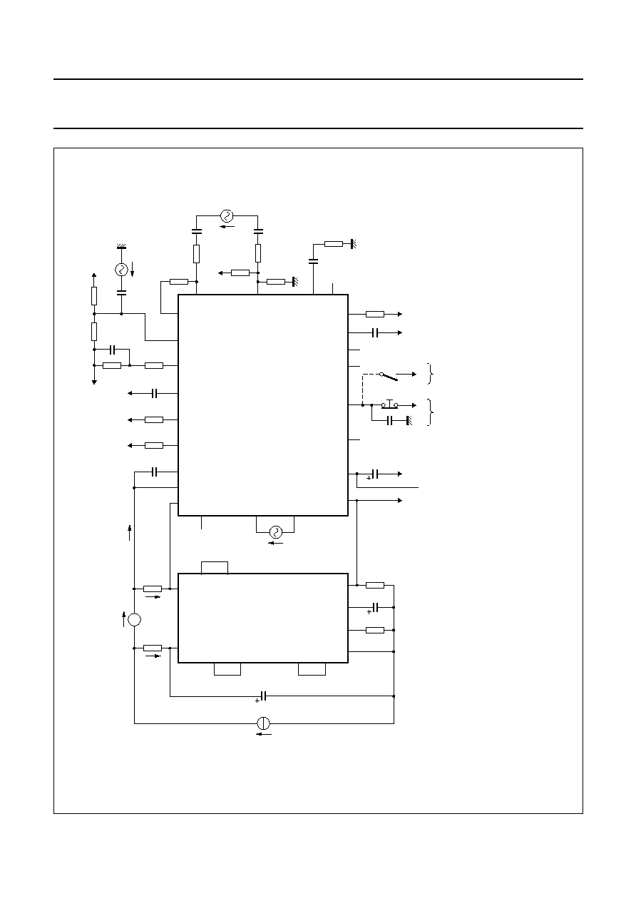
white to force landscape pages to be rotated correctly when browsing through the pdf in the Acrobat reader. white to force landscape pages to be ...
n
dbook, full pagewidth
MGR032
RECEIVING
AMPLIFIER
MUTE
PEAK AND
CURRENT
LIMITER
POWER
AMPLIFIER
START
CIRCUIT
I-STABILIZATION
LOGIC GAIN
CONTROL
LARSEN
LEVEL
LIMITER
SUPPLY
PD
PREAMPLIFIER
LARSEN
LEVEL LIMITER
MUTE
LSI1
LSI2
20
5
DLC
23
2
SUP
3
SDC
4
SREF
6
QLA
11
DTI
15
TEA1060 (VEE)
TEA1060 (QR)
TEA1060
(MIC)
TEA1060
(MIC)
(2)
(1)
(1)
(1)
2
2
2
22
21
QLS2
QLS1
10
9
LAI
+
GSC1
8
GSC2
7
SIC 17
(1)
VBB 24
PD 19
VSS 1
VA 18
LAI
-
VBB
VBB
4
line
TEA1060
(LN)
13
THL2
12
LLC
14
THL1
16
DCA
(1)
VBB
(1)
TEA1085
TEA1085A
Fig.1 Block diagram.
(1) To TEA1060 (SLPE).
(2) See Fig.16.

March 1992
5
Philips Semiconductors
Preliminary specification
Listening-in circuit for line-powered
telephone sets
TEA1085; TEA1085A
PIN CONFIGURATION
SYMBOL PIN
DESCRIPTION
V
SS
1
negative supply
SUP
2
positive supply
SDC
3
supply amplifier decoupling
SREF
4
supply reference input
LSI1
5
loudspeaker amplifier input 1
LSI2
6
loudspeaker amplifier input 2
GSC2
7
logic input 2 for gain select
GSC1
8
logic input 1 for gain select
LAI
-
9
Larsen limiter preamplifier inverting
input
LAI
+
10
Larsen limiter preamplifier
non-inverting input
QLA
11
Larsen limiter preamplifier output
LLC
12
Larsen limiter capacitor
THL2
13
Larsen limiter residual threshold level
THL1
14
Larsen limiter attack delay threshold
level
DTI
15
Larsen limiter detector input
DCA
16
Larsen limiter detector current
adjustment
SIC
17
Larsen limiter current stabilizer
VA
18
V
BB
voltage adjustment
PD
19
power-down input
MUTE
20
MUTE input
QLS1
21
loudspeaker amplifier output 1
QLS2
22
loudspeaker amplifier output 2
DLC
23
dynamic limiter capacitor
V
BB
24
stabilized supply decoupling
Fig.2 Pin configuration.
handbook, halfpage
VSS
SUP
SDC
SREF
LSI1
LSI2
GSC2
GSC1
LAI
-
LAI
+
QLA
LLC
VBB
DLC
QLS2
QLS1
PD
VA
MUTE
SIC
DCA
DTI
THL1
THL2
1
2
3
4
5
6
7
8
9
10
11
12
24
23
22
21
20
19
18
17
16
15
14
13
TEA1085
TEA1085A
MLA415

March 1992
6
Philips Semiconductors
Preliminary specification
Listening-in circuit for line-powered
telephone sets
TEA1085; TEA1085A
FUNCTIONAL DESCRIPTION
Figure 1 illustrates a block diagram of the
TEA1085/TEA1085A with external components and
connections to the transmission IC.
The TEA1085/TEA1085A are bipolar ICs which have been
designed for use in line-powered telephone sets and
provide a listening-in facility for the received line signal via
a loudspeaker. Nearly all the line current can be used for
powering the loudspeaker.
The loudspeaker amplifier consists of a preamplifier, to
amplify the earpiece signal from the transmission circuit
and, a double push-pull output stage to drive the
loudspeaker in the BTL (bridge tied load) or SE (single
ended) configuration. The gain of the preamplifier is
controlled by a dynamic limiter which prevents high
distortion of the loudspeaker signal. This is achieved by
preventing clipping of the loudspeaker signal, with respect
to the supply voltage, and at too low supply current. Two
logic inputs can be used to reduce the gain in 3 steps.
Because of acoustic feedback from the loudspeaker to the
microphone, howling signals (Larsen effect) can occur on
the telephone line and in the loudspeaker. When the
Larsen signal exceeds a voltage and time duration
threshold the Larsen level limiter (LLL) will reduce the
Larsen signal to a low level within a short period of time by
reducing the gain of the receiving preamplifier. This is
achieved by using the microphone signal as an input signal
which is processed in the LLL via a preamplifier and
3rd-order filter.
The MUTE input can be used to enable or disable the
loudspeaker amplifier.
The MUTE function of the TEA1085 has a toggle input to
permit the use of a simple push-button switch.
The MUTE function of the TEA1085A has a logic input to
operate with a microcontroller.
By activating the power-down input the current
consumption of the circuit will be reduced, this enables
pulse dialling or flash (register recall).
An internal start circuit ensures normal start-up of the
transmission IC and start-up of the listening-in IC in the
standby mode.
The TEA1085/TEA1085A are intended for use in
conjunction with a member of the TEA1060 family and
should be connected between LINE and SLPE of the
transmission IC. The transmission characteristics
(impedance, gain settings, for example) are not affected.
The interconnection between the two ICs is illustrated in
Fig.3.
Fig.3 Interconnection of the TEA1085/TEA1085A with the TEA1060.
handbook, full pagewidth
MGR033
TEA1060
VCC
LN
VEE
SLPE
QR
MIC
+
MIC
-
LAI
+
LAI
-
TEA1085
TEA1085A
SREF
SUP
VSS
LSI1
LSI2
QLS
LINE
to TEA1060
(SLPE)

March 1992
7
Philips Semiconductors
Preliminary specification
Listening-in circuit for line-powered
telephone sets
TEA1085; TEA1085A
Supply; SUP, SREF, V
BB
, V
SS
and VA
The line current is divided into I
TR
for the TEA1060 and I
SUP
for the TEA1085/TEA1085A.
The supply arrangement is illustrated in Fig.4.
Fig.4 Supply arrangement.
handbook, full pagewidth
MGR034
TEA1060
VCC
LN
VEE
SLPE
TEA1085
TEA1085A
VSS
VBB
Iline
ITR
SUP
C20
ISUP
IBBO
IBIAS
ICC
R1
R9
R38
VA
R20
VOLTAGE
STABILIZER
TR1
TR2
SREF
Vint
LINE
I
TR
is constant: I
TR
= V
int
/ R20; I
SUP
= I
line
-
I
CC
-
I
TR
Where:
A practical value for R20 is 150
. This value of resistance
produces a value for I
TR
= 2 mA and I
SUP
= I
line
-
3 mA.
The TEA1085/TEA1085A stabilizes its own supply voltage
at V
BB
. Transistor TR1 provides the supplies for the
internal circuits. TR2 is used to minimize the signal
distortion on the line by momentarily diverting the input
current to V
SS
whenever the instantaneous value of the
voltage V
SUP
drops below the supply voltage V
BB
. V
BB
is
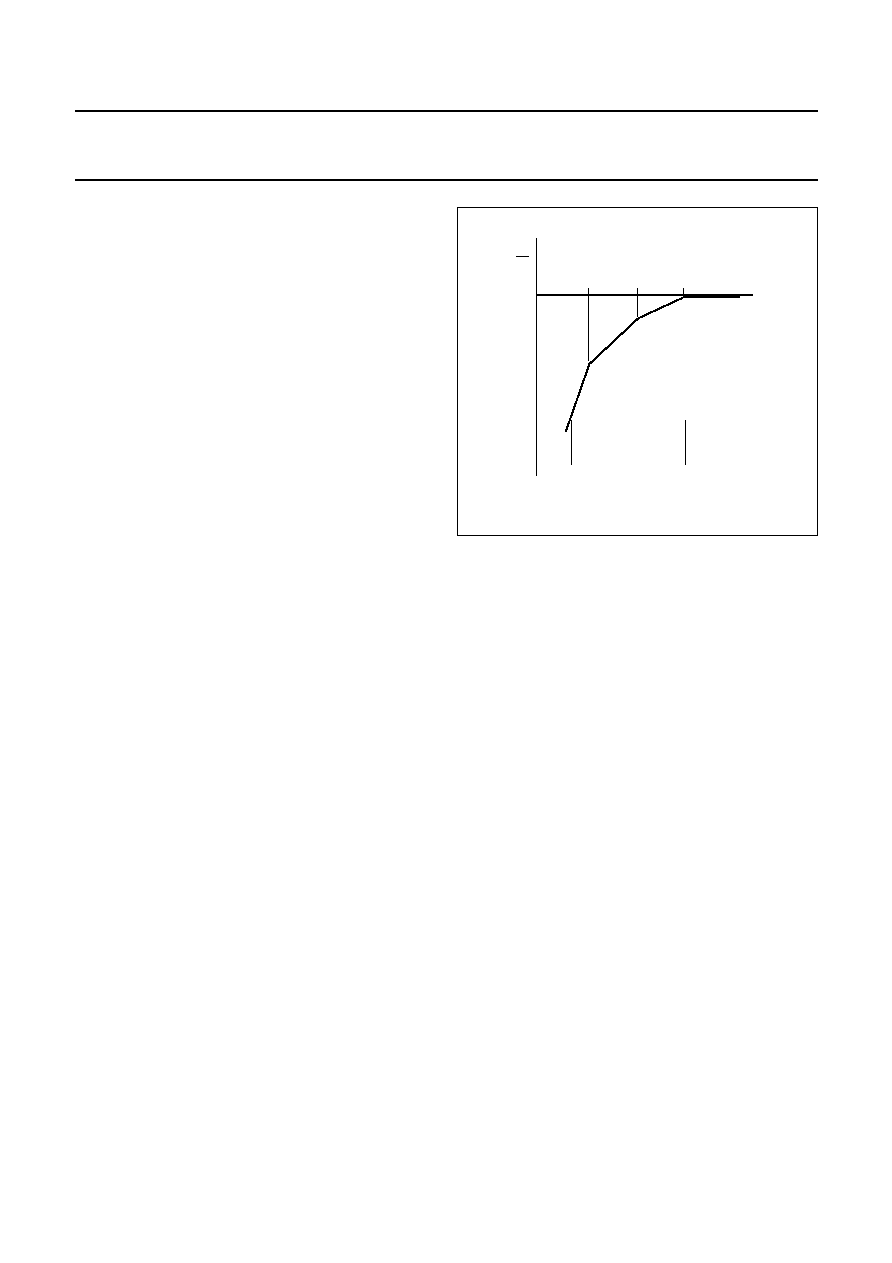
fixed to a typical value of 3.6 V but can be increased by
means of an external resistor (R38) connected between
V
int
is an internal temperature compensated
reference voltage with a typical value of
315 mV between SUP and SREF
R20
is a resistor between SUP and SREF
I
CC
is the internal current consumption of the
TEA106X (
1 mA)
VA and V
SS
or decreased by connecting this resistor
between VA and V
BB
. The minimum level on V
BB
is
restricted to 3.0 V; the level of the V
BB
limiter is also
affected (see application report for further information).
The supply at V
BB
is decoupled by a 470
µ
F capacitor.
The DC voltage (V
SUP
-
V
SS
) is determined by the
transmission IC (V
LN
-
SLPE
); thus:
V
SUP
-
V
SS
= V
LN
-
SLPE
+
V
int
.
The minimum DC voltage that can be applied to this input
is V
BB(max)
+
0.4 V.
Where: V
BB(max)
is the worst case supply voltage (this
depends on the setting of R38, which is connected
between VA and V
SS
).
The internal current consumption of the
TEA1085/TEA1085A (I
SUP0
) is typically 4.2 mA (where
V
SUP
-
V
SS
= 4.5 V, MUTE off). Thus the current available
for powering the loudspeaker is I
SUP
-
I
SUP0
.
The current I
SUP0
consists of a bias current of
0.4 mA for
the circuitry connected to SUP and current I
BB0
of
3.8 mA
which is used for the circuitry connected to V
BB
(see Fig.4).

March 1992
8
Philips Semiconductors
Preliminary specification
Listening-in circuit for line-powered
telephone sets
TEA1085; TEA1085A
Supply amplifier stability (SDC) pin 3
To ensure stability of the TEA1085/TEA1085A, in
combination with a transmission IC of the TEA1060 family,
a 47 pF capacitor connected between SDC and SUP and
a 150
µ
H coil connected between SUP and the positive
line terminal (Fig.16) is required.
Loudspeaker amplifier (LSI1/LSI2 and QLS1/QLS2)
pins 5/6, 21/22
The TEA1085/TEA1085A have symmetrical inputs at LSI1
and LSI2. The input signal is normally taken from the
earpiece output of the transmission circuit via a resistive
attenuator (see Fig.3). The amount of attenuation must be
chosen in accordance with the receive gain of the
transmission IC (which depends on the sensitivity of the
earpiece transducer). The maximum input signal level is
450 mV(RMS) at T
amb
=
+
25
∞
C.
The outputs QLS1 and QLS2 can be used for single ended
drive (SE) or bridge tied load drive (BTL). The output
stages have been optimized for use with a 50
loudspeaker (e.g. Philips type AD2071).
The gain of the amplifier is fixed to
35 dB for the SE drive
and
41 dB for the BTL drive (when the inputs for logic
control are left open-circuit or are connected to V
SS
).
The volume control can be obtained by using a
potentiometer at the input and/or by the logic control
function.
Fig.5
Stabilized supply voltage as a function of
R38.
ndbook, halfpage
5.5
3.5
MGR035
10
10
2
10
3
3.9
4.3
4.7
5.1
R38 (k
)
VBB
(V)
VBB = 3.60 V
Logic gain control (GSC1 and GSC2) pins 7 and 8
The logic inputs GSC1 and GSC2 can be used to reduce
the gain of the loudspeaker amplifier by means of the logic
gain control function in 3 steps of 6 dB.
Table 1
Data for microcontroller drive of logic inputs
Where:
0 = connection to V
SS
or left open-circuit
1 = applying a voltage
V
SS
+
1.5 V
GSC2
GSC1
gain
(dB)
gain reduction
(dB)
0
0
35
0
0
1
28.7
6.3
1
0
22.2
12.2
1
1
17
18

March 1992
9
Philips Semiconductors
Preliminary specification
Listening-in circuit for line-powered
telephone sets
TEA1085; TEA1085A
Dynamic limiter (DLC) pin 23
To prevent distortion of the signal at the loudspeaker
outputs the gain of the amplifier is reduced rapidly when:
∑
the peaks of the signal at the loudspeaker outputs
exceed an internally determined threshold (voltage
limiter)
∑
the DC current into SUP is insufficient (current limiter)
∑
the voltage at V
BB
decreases below an internally
determined threshold, typically 2.9 V (V
BB
limiter)
The time in which the gain reduction is effected is the
'attack time'; this is very short in the first and third instance
and relatively long in the second instance. The circuit will
remain in the gain-reduced condition until the peaks of the
output signal remain below the threshold level. The gain
will then return to a nominal level after a time determined
by the capacitor connected to DLC (release time).
MUTE input (MUTE) pin 20; TEA1085A
This MUTE is provided with a logic input to operate with a
microcontroller for instance.
The loudspeaker amplifier is disabled when the MUTE
input is LOW (connected to V
SS
or open input). A HIGH
level at the MUTE input enables the amplifier in the
listening-in mode.
MUTE input (MUTE) pin 20; TEA1085
The MUTE function is provided with a toggle input and is
designed to switch between the standby condition and the
listening-in condition on the rising edge of the input MUTE
signal (see Fig.6).
In the basic application the MUTE input must be LOW
(connected to V
SS
). A simple push-button can be used to
operate the MUTE toggle (see Fig.7). Debouncing can be
realized by means of a small capacitor connected between
MUTE and V
SS
.
An internal start circuit ensures that the circuit always
starts up in the standby condition.
Fig.6 Mute toggle function of the TEA1085.
handbook, full pagewidth
MGR036
LSI1
QLS1
MUTE
standby
standby
listening-in
Fig.7 Mute switch alternatives with the TEA1085.
handbook, full pagewidth
MLA055
MUTE
MUTE
VBB
10 k
(a) Break contact.
(b) Make contact.

March 1992
10
Philips Semiconductors
Preliminary specification
Listening-in circuit for line-powered
telephone sets
TEA1085; TEA1085A
Power down input (PD) pin 19
During pulse dialling or register recall (timed loop break)
the telephone line is interrupted, thereby breaking the
supply to the transmission and listening-in circuits. The
capacitor connected to V
BB
provides the supply for the
listening-in circuit during the supply breaks.
By making the PD input HIGH during the loop break the
requirement on the capacitor is eased and, consequently,
the internal (standby) current consumption I
BBO
(Fig.4) at
V
BB
is reduced from 3.8 mA to 400
µ
A typical. So that the
transmission circuit is not affected transistors TR1 and
TR2 are inhibited and the bias current is reduced from
0.4 mA to
55
µ
A with V
SUP
= 4.5 V in the following
equation:
I
SUP(PD)
= I
BIAS(PD)
= (V
SUP
-
2V
d
) / Ra
(where 4.2 V
<
V
SUP
<
V
BB
+
3 V)
2V
d
= the voltage drop across 2 internal diodes (
1.3 V)
Ra = an internal resistor of typical 60 k
Larsen limiter current stabilizer (SIC) pin 17
A current reference is set by resistor R36 between SIC and
V
SS
. The preferred value is 120 k
. The internal reference
current is given by the following equation:
I
SIC
= 1.25 / R36; when R36 = 120 k
, I
SIC
= 10.5
µ
A
Changing the value of R36 will affect the timing of the
Larsen level limiter system.
Larsen limiter preamplifier (LAI1/LAI2 and QLA) pins
9/10 and 11
This circuit amplifies the microphone signal to a level
suitable for the Larsen limiter detector. The gain is set by
external components (see Fig.8).
Normally the gain is set to the same level as the
microphone amplifier of the transmission circuit, this
ensures that the output signal level at output QLA is equal
to the line signal level.
The gain between QLA and the microphone input is given
by the following equation (the high-pass filter is not taken
into account):
A
pre
= V
QLA
/ V
M
= R29 / R26; in the basic application
R25 = R26 = 10 k
The gain can be adjusted between 30 dB (R29 = 316 k
)
and 52 dB (R29 = 4 M
). The impedance result of R28 and
R27 in parallel must be equal to R29
(e.g. R27 = R28 = 2
◊
R29).
Fig.8 Larsen limiter preamplifier and voltage/current converter.
handbook, full pagewidth
MGR037
LAI
+
LAI
-
+
-
+
-
R25
R26
R29
C22
C23
VM
DTI
DCA
IDCA
THL1
THL2
R27
QLA
C24
R30
R33
R32
C25
R31
R35
R34
VQLA
VBB
VSS
VBB
R28
LARSEN
DETECTOR
LLC
March 1992
11
Philips Semiconductors
Preliminary specification
Listening-in circuit for line-powered
telephone sets
TEA1085; TEA1085A
Larsen limiter detector (DTI and DCA) pins 15 and 16
The QLA output signal is AC coupled to the detector input
DTI. DTI is biased by potential divider R30 and R31. The
voltage applied to DTI of the Larsen level limiter is
converted into a current for further processing in this
circuit. Current adjustment is achieved using the network
connected between DCA and V
BB
(see Fig.8).
The equation for DC current is:
The equation for AC current is:
In the basic application:
R30 = 100 k
, R31 = 220 k
, R33 = 500
, R32 = 100 k
and C25 = 330 nF
This results in I
DCA
= 11
µ
A and the equation:
High-pass filter
A third order high-pass filter is created between the
microphone input voltage and the current flowing into
DCA. The cut-off frequencies (see Fig.9) of the three
sections are:
Where: R25 = R26 and C22 = C23
The filter reduces the sensitivity of the system to own
speech.
Normal speech is in the frequency range 300 Hz to
3400 Hz, however, the Larsen signal normally occurs at a
frequency
>
3 kHz.
With the component values as used in the basic
application (see Fig.16); f1 = 500 Hz, f2 = 1 kHz and
f3 = 3 kHz
I
DCA
R30
R30
R31
+
-----------------------------
V
BB
1
R32
R33
+
-----------------------------
◊
◊
=
i
DCA
V
DTI
R33
------------
for f >
1
2
---
R33 C25
=
i
DCA
V
DTI
------------
2 (mA/V)
=
f1
1
2
R
eg
C24
-----------------------------
where R
eq
R30
R31
◊
R30
R31
+
-----------------------------
=
=
f2
1
2
R33C24
------------------------------
=
f3
1
2
R26C23
------------------------------
1/(2
R25C22
)
=
=
Where:
Larsen limiter capacitor (LLC) pin 12
A 1
µ
F capacitor (C26) is connected externally between
V
SS
and LLC to determine the attack and release timing of
the Larsen level limiter in the listen-in and Larsen mode.
The timing is also dependent on the value of the resistor
connected between SIC and V
SS
.
Larsen level limiter threshold (THL1 and THL2) pins
13 and 14
When the signal at DTI exceeds the first threshold level the
capacitor connected to LLC will start to discharge. The first
threshold level is determined by the value of the resistor,
R35, connected to THL1 and V
SS
. The amount of
discharge of C26 depends on how much the level of the
signal at DTI exceeds the first threshold level (for normal
speech the discharge is small).
The Larsen effect is generally defined as a signal level of
100 mV(RMS), on line, for a period of more than 100 ms.
The Larsen signal must be reduced to a low level within
200 ms. For Larsen signal levels (f
>
f3 in Fig.9) of
100 mV(RMS) at DTI and, with the component values of
Fig.16, the system will switch from the listen-in mode to the
Larsen mode in a time period of 100 ms to 200 ms;
consequently, the initial Larsen effect will last only for a
short period of time.
Fig.9 Third-order high-pass filter.
handbook, halfpage
MGR038
20 log
(dB)
g
go
20 log f
f3
f2
f1
0
12 dB per octave
6 dB per octave
18 dB per octave
speech
Larsen
g
i
DCA
V
m
-----------
=
g
o
A
pre
R33
-----------
=

March 1992
12
Philips Semiconductors
Preliminary specification
Listening-in circuit for line-powered
telephone sets
TEA1085; TEA1085A
This reaction time is the 'attack delay time' and ensures
minimum sensitivity of the system for own speech.
The first threshold level at DTI is determined by the
equation:
Where: I
DCA
= the DC current into DCA
With the component values given in Fig.16, I
DCA
= 11
µ
A
thus V
DTI1
= 18.8 mV.
Listen-in mode
During normal speech the discharge of the capacitor
connected to LLC is not sufficient to reach the threshold
level whereby the system switches to the Larsen mode.
This is because normal speech is not continuous, the
discharge of C26 is slow (attack delay) and the charge is
fast.
The slope of V
LLC
during charge is given in the equation:
With C26 = 1
µ
F and R36 = 120 k
this results in
S
1i
= 10 V/s.
Discharge of the capacitor at LLC occurs when the signal
at DTI exceeds V
DTI1
, thus for a continuous signal at DTI
the attack delay time t
ad
(see Fig.10) is determined by the
equation:
Where k = t
1
/ T
The duty cycle is determined by the time in which the first
threshold level (V
DTI1
) is exceeded by the signal level at
DTI (see Fig.11) thus for large signals; k
0.5.
With the component values given in Fig.16; k
0.457 for
signals
100 mV(RMS).
Consequently 120 ms
t
ad
160 ms, for
V
DTI
100 mV(RMS)
V
DTI1
1.25
R25
-----------
I
DCA
2
------------
≠
2
R33
◊
◊
if f > f3 in Fig.9
(
)
=
S
1i
V
LLC
-----------------
=
1.25
C26
R36
◊
-----------------------------
V s
/
(
)
=
t
ad
C26
R36
◊
2
3
k
1
≠
◊
(
)
◊
--------------------------------------
=
Larsen mode
After the 'attack delay time' the circuit switches from the
listen-in mode to the Larsen mode. The gain of the
loudspeaker amplifier is reduced quickly to a value
(t
LAa
= Larsen attack time, see Fig.10) whereby the
residual Larsen signal is determined by a second
threshold level. This level can be set by resistor R34
connected between THL2 and V
SS
. The second threshold
level must always be selected at a lower level than the first
threshold level thus R34
>
R35.
The time taken to effect gain reduction is very short. In the
Larsen mode the circuit acts as a dynamic limiter with peak
detector and regulates the gain so that the signal level at
DTI is determined by the second threshold level V
DTI2
.
The second threshold level at DTI is determined by the
equation:
Where: I
DCA
= the DC current into DCA
With the component values given in Fig.16,
V
DTI2
= 6.9 mV.
The charge current in the Larsen mode is reduced to half
the charge current in the listen-in mode.
The slope of V
LLC
during charge (see Fig.10) is given in the
equation:
Where: C26 = 1
µ
F and R36 = 100 k
, S
la
= 5 V/s
When the Larsen effect stops (total open-loop gain
<
1) the
gain of the loudspeaker amplifier will return to its normal
value in a time period known as the 'Larsen release time'
(t
LAr
). This time period is determined by capacitor C26
connected to LLC and resistor R36 connected to SIC.
Where: C26 = 1
µ
F and R36 = 120 k
, t
LAr
= 250 ms
In practice the choice of the threshold levels (determined
by R35 and R34) depends on the sensitivity of the
microphone and loudspeaker, the send and receive gains,
sidetone suppression and the acoustical properties which
are determined by the cabinet of the telephone set.
V
DTI2
1.25
R34
-----------
I
DCA
2
------------
≠
2
R33
if f > f3 in Fig.9
(
)
◊
◊
=
S
la
V
LLC
-----------------
1.25
2
C26
◊
R34
◊
--------------------------------------
V s
/
(
)
=
=

March 1992
13
Philips Semiconductors
Preliminary specification
Listening-in circuit for line-powered
telephone sets
TEA1085; TEA1085A
Fig.10 Dynamic behaviour of Larsen limiter (in open-loop condition).
Where:
Change of receive gain
G
v
G
vo
----------
=
Nominal receive gain = 20 log G
vo
= 35 dB
handbook, full pagewidth
MGR039
VDTI
VLLC
slope Sli
slope Sla
tad
tLAr
0.5 V
1
0 V
listen-in mode
listen-in mode
Larsen mode
tLAa
0.63 V
handbook, full pagewidth
MGR040
-
VDTI
VDTI1
t1
T
VDTI
^
Fig.11 Definition of duty cycle k.
Where:
k
t
1
T
----
=
k
0.5
≠
arc
V
DTI1
V
^
DTI
---------------
sin
----------------------------------------
=

March 1992
14
Philips Semiconductors
Preliminary specification
Listening-in circuit for line-powered
telephone sets
TEA1085; TEA1085A
LIMITING VALUES
In accordance with the Absolute Maximum System (IEC 134)
THERMAL RESISTANCE
Note
1. Device mounted on a glass epoxy board 40.1
◊
19.1
◊
1.5 mm.
SYMBOL
PARAMETER
CONDITIONS
MIN.
MAX.
UNIT
V
SUP
positive supply voltage
continuous
-
12
V
during switch-on or line interruption
-
13.2
V
repetitive supply voltage from 1 ms to 5 s
with 12
current
limiting resistor in
series with supply
-
28
V
V
SREF
supply reference voltage
V
SS
-
0.5
V
SUP
+
0.5
V
V
n
voltage on all other pins
V
SS
-
0.5
V
BB
+
0.5
V
I
SUP
supply current
TEA1085/TEA1085A
see Fig.12
-
120
mA
TEA1085T/TEA1085AT
see Fig.13
-
120
mA
P
tot
total power dissipation
T
amb
= 75
∞
C;
T
j
= 125
∞
C
TEA1085/TEA1085A
-
1
W
TEA1085T/TEA1085AT
-
666
mW
T
amb
operating ambient temperature range
-
25
+
75
∞
C
T
stg
storage temperature range
-
40
+
125
∞
C
T
j
junction temperature
-
+
125
∞
C
SYMBOL
PARAMETER
CONDITIONS
THERMAL
RESISTANCE
R
th j-a
from junction to ambient in free air
TEA1085/TEA1085A
50 K/W
TEA1085T/TEA1085AT
note 1
75 K/W

March 1992
15
Philips Semiconductors
Preliminary specification
Listening-in circuit for line-powered
telephone sets
TEA1085; TEA1085A
Fig.12 TEA1085/TEA1085A safe operating area.
(1) T
amb
= 55
∞
C; P
tot
= 1.4 W.
(2) T
amb
= 65
∞
C; P
tot
= 1.2 W.
(3) T
amb
= 75
∞
C; P
tot
= 1.0 W.
handbook, halfpage
2
12
130
30
50
MGR041
70
90
110
4
6
8
10
VSUP (V)
(2)
(3)
(1)
ISUP
(mA)
Fig.13 TEA1085T/TEA1085AT safe operating
area.
(1) T
amb
= 35
∞
C; P
tot
= 1.2 W.
(2) T
amb
= 45
∞
C; P
tot
= 1.07 W.
(3) T
amb
= 55
∞
C; P
tot
= 0.93 W.
(4) T
amb
= 65
∞
C; P
tot
= 0.8 W.
(5) T
amb
= 75
∞
C; P
tot
= 0.666 W.
handbook, halfpage
2
12
130
30
50
MGR042
70
90
110
4
6
8
10
VSUP (V)
(2)
(3)
(4)
(5)
(1)
ISUP
(mA)
March 1992
16
Philips Semiconductors
Preliminary specification
Listening-in circuit for line-powered
telephone sets
TEA1085; TEA1085A
CHARACTERISTICS
V
SREF
= 4.2 V; V
SS
= 0 V; I
SUP
= 15 mA; V
SUP
= 0 V(RMS); f = 800 Hz; T
amb
= 25
∞
C; PD = LOW; MUTE (TEA1085) =
OFF (listening-in mode); MUTE (TEA1085A) = HIGH (listening-in mode); GSC1 = GSC2 = LOW; 50
loudspeaker;
no R38; test circuit Fig.14; unless otherwise specified
SYMBOL
PARAMETER
CONDITIONS
MIN.
TYP.
MAX.
UNIT
Supplies
V
SUP
minimum DC input voltage
-
V
BB
+
0.7
-
V
V
SUP-SREF
internal reference voltage
275
315
355
mV
V
BB
stabilized supply voltage
no R38; I
SUP
= 15 mA
3.4
3.6
3.8
V
V
BB
variation from
I
SUP
= 15 to 120 mA
-
10
-
mV
R38 = 39.2 k
between
pins V
SS
and VA;
V
SREF
= 5.2 V;
I
SUP
= 15 mA
4.2
4.45
4.7
V
V
BB
/
T
variation with temperature
no R38; I
SUP
= 15 mA
tbf
-
0.2
tbf
V
I
SUP
minimum operating current
-
4.2
5.5
mA
THD
distortion of AC signal on SUP V
SUP(RMS)
= 1 V
-
0.3
-
%
V
no(RMS)
noise between SUP and V
EE
-
-
72
-
dBmp
current consumption in
power-down condition
PD = HIGH
I
SUP
V
SUP
= 4.5 V
-
55
75
µ
A
I
BB
V
BB
= 3.6 V
-
400
550
µ
A
Loudspeaker amplifier inputs LSI1 and LSI2
|
Z
i
|
input impedance
single ended
7.5
9.5
11.5
k
differential
15
19
23
k
G
v
voltage gain with 50
load
I
SUP
= 15 mA;
V
i
= 1.8 mV(RMS)
single ended
34
35
36
dB
BTL output
39.9
40.9
41.9
dB
G
v
variation with signal level
I
SUP
= 50 mA;
V
i
= 1.8 mV(RMS) and
14 mV(RMS)
single ended
-
+
0.1
0.4
dB
BTL output
-
+
0.2
0.6
dB
G
v
variation with frequency
referred to 1 kHz
f = 300 Hz and 3400 Hz;
V
i
= 1.8 mV(RMS)
single ended
-
±
0.1
-
dB
BTL output
-
±
0.1
-
dB
G
v
variation with temperature
referred to 25
∞
C
T
amb
=
-
25 to
+
75
∞
C
single ended
-
±
0.4
-
dB
BTL output
-
±
0.5
-
dB

March 1992
17
Philips Semiconductors
Preliminary specification
Listening-in circuit for line-powered
telephone sets
TEA1085; TEA1085A
Loudspeaker outputs QLS1 and QLS2
V
o(p-p)
output voltage (peak-to-peak
value)
V
i
= 22 mV(RMS)
single ended
I
SUP
= 9 mA; note 1
1.2
1.45
-
V
I
SUP
= 17 mA; note 2
2.5
2.9
-
V
bridge tied load
I
SUP
= 23.5 mA; note 2
2.5
2.9
-
V
I
SUP
= 32 mA; note 3
3.5
4.0
-
V
THD
total harmonic distortion
V
i
= 22 mV(RMS)
single ended
I
SUP
= 9 mA
-
0.4
2
%
I
SUP
= 17 mA
-
0.7
2
%
bridge tied load
I
SUP
= 23.5 mA
-
0.4
2
%
V
o(p-p)
output voltage (peak-to-peak
value)
V
i
= 22 mV(RMS)
single ended
I
SUP
= 17 mA;
V
SUP
-
V
EE
= 1 V(RMS)
1.75
2.15
-
V
Dynamic limiter
THD
total harmonic distortion
V
i
= 22 mV(RMS)
+
10 dB
single ended
I
SUP
= 9 mA
-
0.5
10
%
I
SUP
= 17 mA
-
1.2
10
%
bridge tied load
I
SUP
= 23.5 mA
-
0.6
10
%
t
att
dynamic behaviour of limiter
attack time; V
i
jumps from
10 mV(RMS) to 65 mV(RMS)
single ended load
voltage limiter
I
SUP
= 17 mA
-
2
5
ms
current limiter
I
SUP
= 12 mA
-
500
tbf
ms
V
BB
limiter
I
SUP
= 9 mA
-
10
-
ms
t
rel
release time; V
i
jumps from
65 mV(RMS) to 10 mV(RMS)
I
SUP
= 17 mA
tbf
75
tbf
ms
V
BBO
threshold V
BB
limiter below
which gain reduction starts
I
SUP
= 9 mA
tbf
2.95
tbf
V
V
no(RMS)
noise output voltage
1 k
between inputs
LSI1, LSI2;
psophometrically
weighted (P53 curve)
single ended
-
170
-
µ
V
bridge tied load
-
350
-
µ
V
Logic gain control
G
v
reduction of voltage gain
V
i
= 1.8 mV(RMS)
GSC2 = 0, GSC1 = 1
5.8
6.3
6.8
dB
GSC2 = 1, GSC1 = 0
11.7
12.2
12.7
dB
GSC2 = 1, GSC1 = 1
17
18
19
dB
SYMBOL
PARAMETER
CONDITIONS
MIN.
TYP.
MAX.
UNIT
March 1992
18
Philips Semiconductors
Preliminary specification
Listening-in circuit for line-powered
telephone sets
TEA1085; TEA1085A
Larsen limiter preamplifier
operational amplifier
G
v0
open-loop gain
-
92
-
dB
f
p1
1st pole
-
120
-
Hz
f
p2
2nd pole
-
3.3
-
MHz
G
B
unity gain bandwidth
-
4
-
MHz
G
v
voltage gain
f = 3 kHz;
R26 = 10 k
;
R29 = 4 M
51
52
53
dB
G
v
gain adjustment range
30
-
52
dB
Larsen limiter detector
voltage to current convertor
V
DCA
-V
DTI
DC offset voltage
V
BB
-
V
DTI
= 1 V
-
25
1
+
25
mV
G
v
voltage gain from DTI to DCA
V
DTI
= 100 mV(RMS);
f = 3 kHz
tbf
-
0.8
tbf
dB
V
THL1
DC voltage at THL1
R35 = 51 k
1.8
1.25
1.33
V
V
THL2
DC voltage at THL2
R34 = 100 k
1.8
1.25
1.33
V
dynamic behaviour with a
burst at DTI
f = 3 kHz; see Fig.15
t
LIr
listen-in release time
see Fig.15(a)
tbf
40
tbf
ms
t
ad
attack delay time
see Fig.15(b)
V
DTI
jumps from
0 to 100 mV (RMS value)
-
160
200
ms
V
DTI
jumps from
0 to 1 V (RMS value)
100
120
-
ms
t
LAa
Larsen attack time
see Fig.15(b);
V
DTI
= 100 mV(RMS)
-
20
tbf
ms
t
LAr
Larsen release time
see Fig.15(b)
V
DTI
jumps from
100 mV to 0 mV (RMS
value)
tbf
250
tbf
ms
V
LLC
DC voltage at LLC
V
DTI
= 0 V
1.75
1.9
2.0
V
-
V
LLC
reduction of V
LLC
to attack
Larsen mode
0.59
0.63
0.68
V
G
v
gain reduction
V
LLC
= 0.7 V
60
tbf
tbf
dB
SYMBOL
PARAMETER
CONDITIONS
MIN.
TYP.
MAX.
UNIT

March 1992
19
Philips Semiconductors
Preliminary specification
Listening-in circuit for line-powered
telephone sets
TEA1085; TEA1085A
Notes
1. Typical output power is 5 mW into 50
2. Typical output power is 20 mW into 50
3. Typical output power is 40 mW into 50
MUTE input; TEA1085
(toggle function, positive edge
triggered set-reset flip-flop)
V
IL
LOW level input voltage
0
-
0.3
V
V
IH
HIGH level input voltage
1.5
-
V
BB
+
0.4
V
I
MUTE
input current
MUTE = LOW
-
-
22
-
28
µ
A
t
W
minimum input pulse width
-
50
-
µ
s
P
R
minimum pulse repetition time
-
2
-
ms
V
BB(MUTE)
supply voltage below which
MUTE toggle is reset
tbf
2
tbf
V
G
v
reduction of gain from LSI1,
LSI2 to QLS1, QLS2
MUTE = ON
60
100
-
dB
MUTE input; TEA1085A
V
IL
LOW level input voltage
0
-
0.3
V
V
IH
HIGH level input voltage
1.5
-
V
BB
+
0.4
V
I
MUTE
input current
MUTE = HIGH
-
10
20
µ
A
G
v
reduction of gain from LSI1,
LSI2 to QLS1, QLS2
MUTE = HIGH
60
100
-
dB
Power down input
V
IL
LOW level input voltage
0
-
0.3
V
V
IH
HIGH level input voltage
1.5
-
V
BB
+
0.4
V
I
PD
input current
PD = HIGH
-
2.3
2.8
µ
A
Logic inputs GSC1 and GSC2
V
IL
LOW level input voltage
0
-
0.3
V
V
IH
HIGH level input voltage
1.5
-
V
BB
+
0.4
V
I
GSC
input current
GSC = HIGH
-
6
8
µ
A
SYMBOL
PARAMETER
CONDITIONS
MIN.
TYP.
MAX.
UNIT
March
1992
20
Philips Semiconductors
Preliminary specification
Listening-in circuit for line-powered
telephone sets
TEA1085; TEA1085A
This text is here in white to force landscape pages to be rotated correctly when browsing through the pdf in the Acrobat reader.This text is here in
_
white to force landscape pages to be rotated correctly when browsing through the pdf in the Acrobat reader.This text is here inThis text is here in
white to force landscape pages to be rotated correctly when browsing through the pdf in the Acrobat reader. white to force landscape pages to be ...
agewidth
MGR043
3
2
5
6
6
5
19
9
7
8
10
9
16
18
15
1
4
2
3
14
C3
C1
C20
R9
R5
R1
R20
C21
R35
R28
(1)
(1)
(1)
C28
(1)
R36
(1)
13
R34
16
R33
R29
R26
R31
R30
R32
(1)
(1)
12
C26
11
15
1
24
18
8
7
20
17
23
C23
C24
C27
C25
(1)
VBB
10
21
22
R27
R25
C22
VBB
VBB
VBB
C31
(1)
for
TEA1085
for
TEA1085A
TEA1060
TEA1085
TEA1085A
RL
50
A
IIN
ISUP
Iline
VLSI
VDTI
ILN
ICC
Vm
Fig.14 Test circuit.
The DC current is divided as follows:
The pins not shown in the TEA1060 are left open. An impedance in series with pin SUP (e.g. an ammeter)
should be avoided as it interferes with the value of I
LN
.
I
SUP
I
IN
V
SUP
SREF
≠
R20
-------------------------------
≠
=
I
LN
V
SUP
SREF
≠
R20
-------------------------------
=
(1) To TEA1060 (SLPE)
March 1992
21
Philips Semiconductors
Preliminary specification
Listening-in circuit for line-powered
telephone sets
TEA1085; TEA1085A
Table 2
Component values in test circuit Fig.14
COMPONENT
CONDITION
VALUE
UNIT
Resistor
R1
620
R5
3.6
k
R9
20
R20
150
R25
10
k
R26
10
k
R27
8
M
R28
8
M
R29
4
M
R30
100
k
R31
220
k
R32
100
k
R33
500
R34
100
k
R35
51
k
R36
120
k
Capacitor
C1
100
µ
F
C3
4.7
µ
F
C20
470
µ
F
C21
68
pF
C22
2.2
µ
F
C23
2.2
µ
F
C24
100
nF
C25
330
nF
C26
1
µ
F
C27
220
µ
F
C28
330
nF
C31
TEA1085 only
10
nF

March 1992
22
Philips Semiconductors
Preliminary specification
Listening-in circuit for line-powered
telephone sets
TEA1085; TEA1085A
Fig.15 Test signals for Larsen level limiter.
(b) Attack delay (t
ad
), Larsen attack time (t
LAa
),
Larsen release time (t
LAr
);
V
DTI
= 100 mV(RMS) and 1 V(RMS); f = 3 kHz.
handbook, full pagewidth
MGR044
0.63 V
VLLCO
VLLC
VDTI
tad
200 ms
tLAr
tLAa
VLLC
100 ms
tLIr
VDTI
(a) Listen-in release time (t
LIr
);
V
DTI
= 100 mV(RMS); f = 3 kHz.
March
1992
23
Philips Semiconductors
Preliminary specification
Listening-in circuit for line-powered
telephone sets
TEA1085; TEA1085A
This text is here in white to force landscape pages to be rotated correctly when browsing through the pdf in the Acrobat reader.This text is here in
_
white to force landscape pages to be rotated correctly when browsing through the pdf in the Acrobat reader.This text is here inThis text is here in
white to force landscape pages to be rotated correctly when browsing through the pdf in the Acrobat reader. white to force landscape pages to be ...
APPLICA
TION INFORMA
TION
handbook, full pagewidth
MLA039
DIALLER
TONE
DP
DP
DP
LINE
DP
interrupt
13
6
5
19
9
7
5
8
12
10
16
18
15
1
4
2
3
14
C3
C2
C1
C11
C29
C30
C32
C20
R38
R9
R24
RV20
R1
R20
L1
C21
R35
R28
(1)
(1)
(1)
C28
(1)
(1)
(1)
R36
(1)
13
R34
16
R33
R29
R26
R31
R30
R32
(1)
(1)
12
C26
11
15
1
24
18
8
7
20
17
23
C24
C23
C27
C25
(1)
VBB
10
21
22
R27
R25
C22
VBB
VBB
VBB
C31
(1)
for
TEA1085
for
TEA1085A
to TEA1060
pins 7 and 8
TEA1060
TEA1085
TEA1085A
Fig.16 Basic application of TEA1085/TEA1085A and TEA1060.
(1) To TEA1060 (SLPE).
March 1992
24
Philips Semiconductors
Preliminary specification
Listening-in circuit for line-powered
telephone sets
TEA1085; TEA1085A
The basic application circuit of the TEA1085/TEA1085A is illustrated in Fig.16. Only the most important components of
the TEA1060 part are shown, other components and their values are given in the TEA1060 Data sheet.
The supply pin (V
BB
) of the TEA1085/TEA1085A can also be used to supply peripheral circuits (e.g. microcontrollers,
diallers etc.). Further information will be published in the TEA1085 application report.
Table 3
Component values in application circuit Fig.16
Note
1. Value depends on the gain setting of the transmission circuit.
COMPONENT
CONDITION
VALUE
UNIT
Resistor
R20
150
R24
note 1
1
k
R25
10
k
R26
10
k
R27
note 1
3.3
M
R28
note 1
3.3
M
R29
note 1
1.65
M
R30
100
k
R31
220
k
R32
100
k
R33
500
R34
100
k
R35
51
k
R36
120
k
RV20
note 1
1
k
Capacitor
C11
4.7
nF
C20
470
µ
F
C21
47
pF
C22
4.7
nF
C23
4.7
nF
C24
4.7
nF
C25
330
nF
C26
1
µ
F
C27
47
µ
F
C28
330
nF
C29
220
nF
C30
220
nF
C31
TEA1085 only 10
nF
Coil
L1
150
µ
H

March 1992
25
Philips Semiconductors
Preliminary specification
Listening-in circuit for line-powered
telephone sets
TEA1085; TEA1085A
PACKAGE OUTLINES
UNIT
A
max.
1
2
b
1
c
D
E
e
M
H
L
REFERENCES
OUTLINE
VERSION
EUROPEAN
PROJECTION
ISSUE DATE
IEC
JEDEC
EIAJ
mm
inches
DIMENSIONS (inch dimensions are derived from the original mm dimensions)
SOT101-1
92-11-17
95-01-23
A
min.
A
max.
b
w
M
E
e
1
1.7
1.3
0.53
0.38
0.32
0.23
32.0
31.4
14.1
13.7
3.9
3.4
0.25
2.54
15.24
15.80
15.24
17.15
15.90
2.2
5.1
0.51
4.0
0.066
0.051
0.021
0.015
0.013
0.009
1.26
1.24
0.56
0.54
0.15
0.13
0.01
0.10
0.60
0.62
0.60
0.68
0.63
0.087
0.20
0.020
0.16
051G02
MO-015AD
M
H
c
(e )
1
M
E
A
L
seating plane
A
1
w
M
b
1
e
D
A
2
Z
24
1
13
12
b
E
pin 1 index
0
5
10 mm
scale
Note
1. Plastic or metal protrusions of 0.25 mm maximum per side are not included.
Z
max.
(1)
(1)
(1)
DIP24: plastic dual in-line package; 24 leads (600 mil)
SOT101-1

March 1992
26
Philips Semiconductors
Preliminary specification
Listening-in circuit for line-powered
telephone sets
TEA1085; TEA1085A
UNIT
A
max.
A
1
A
2
A
3
b
p
c
D
(1)
E
(1)
(1)
e
H
E
L
L
p
Q
Z
y
w
v
REFERENCES
OUTLINE
VERSION
EUROPEAN
PROJECTION
ISSUE DATE
IEC
JEDEC
EIAJ
mm
inches
2.65
0.30
0.10
2.45
2.25
0.49
0.36
0.32
0.23
15.6
15.2
7.6
7.4
1.27
10.65
10.00
1.1
1.0
0.9
0.4
8
0
o
o
0.25
0.1
DIMENSIONS (inch dimensions are derived from the original mm dimensions)
Note
1. Plastic or metal protrusions of 0.15 mm maximum per side are not included.
1.1
0.4
SOT137-1
X
12
24
w
M
A
A
1
A
2
b
p
D
H
E
L
p
Q
detail X
E
Z
c
L
v
M
A
13
(A )
3
A
y
0.25
075E05
MS-013AD
pin 1 index
0.10
0.012
0.004
0.096
0.089
0.019
0.014
0.013
0.009
0.61
0.60
0.30
0.29
0.050
1.4
0.055
0.419
0.394
0.043
0.039
0.035
0.016
0.01
0.25
0.01
0.004
0.043
0.016
0.01
e
1
0
5
10 mm
scale
SO24: plastic small outline package; 24 leads; body width 7.5 mm
SOT137-1
95-01-24
97-05-22

March 1992
27
Philips Semiconductors
Preliminary specification
Listening-in circuit for line-powered
telephone sets
TEA1085; TEA1085A
SOLDERING
Introduction
There is no soldering method that is ideal for all IC
packages. Wave soldering is often preferred when
through-hole and surface mounted components are mixed
on one printed-circuit board. However, wave soldering is
not always suitable for surface mounted ICs, or for
printed-circuits with high population densities. In these
situations reflow soldering is often used.
This text gives a very brief insight to a complex technology.
A more in-depth account of soldering ICs can be found in
our
"Data Handbook IC26; Integrated Circuit Packages"
(order code 9398 652 90011).
DIP
S
OLDERING BY DIPPING OR BY WAVE
The maximum permissible temperature of the solder is
260
∞
C; solder at this temperature must not be in contact
with the joint for more than 5 seconds. The total contact
time of successive solder waves must not exceed
5 seconds.
The device may be mounted up to the seating plane, but
the temperature of the plastic body must not exceed the
specified maximum storage temperature (T
stg max
). If the
printed-circuit board has been pre-heated, forced cooling
may be necessary immediately after soldering to keep the
temperature within the permissible limit.
R
EPAIRING SOLDERED JOINTS
Apply a low voltage soldering iron (less than 24 V) to the
lead(s) of the package, below the seating plane or not
more than 2 mm above it. If the temperature of the
soldering iron bit is less than 300
∞
C it may remain in
contact for up to 10 seconds. If the bit temperature is
between 300 and 400
∞
C, contact may be up to 5 seconds.
SO
R
EFLOW SOLDERING
Reflow soldering techniques are suitable for all SO
packages.
Reflow soldering requires solder paste (a suspension of
fine solder particles, flux and binding agent) to be applied
to the printed-circuit board by screen printing, stencilling or
pressure-syringe dispensing before package placement.
Several techniques exist for reflowing; for example,
thermal conduction by heated belt. Dwell times vary
between 50 and 300 seconds depending on heating
method. Typical reflow temperatures range from
215 to 250
∞
C.
Preheating is necessary to dry the paste and evaporate
the binding agent. Preheating duration: 45 minutes at
45
∞
C.
W
AVE SOLDERING
Wave soldering techniques can be used for all SO
packages if the following conditions are observed:
∑
A double-wave (a turbulent wave with high upward
pressure followed by a smooth laminar wave) soldering
technique should be used.
∑
The longitudinal axis of the package footprint must be
parallel to the solder flow.
∑
The package footprint must incorporate solder thieves at
the downstream end.
During placement and before soldering, the package must
be fixed with a droplet of adhesive. The adhesive can be
applied by screen printing, pin transfer or syringe
dispensing. The package can be soldered after the
adhesive is cured.
Maximum permissible solder temperature is 260
∞
C, and
maximum duration of package immersion in solder is
10 seconds, if cooled to less than 150
∞
C within
6 seconds. Typical dwell time is 4 seconds at 250
∞
C.
A mildly-activated flux will eliminate the need for removal
of corrosive residues in most applications.
R
EPAIRING SOLDERED JOINTS
Fix the component by first soldering two diagonally-
opposite end leads. Use only a low voltage soldering iron
(less than 24 V) applied to the flat part of the lead. Contact
time must be limited to 10 seconds at up to 300
∞
C. When
using a dedicated tool, all other leads can be soldered in
one operation within 2 to 5 seconds between
270 and 320
∞
C.

March 1992
28
Philips Semiconductors
Preliminary specification
Listening-in circuit for line-powered
telephone sets
TEA1085; TEA1085A
DEFINITIONS
LIFE SUPPORT APPLICATIONS
These products are not designed for use in life support appliances, devices, or systems where malfunction of these
products can reasonably be expected to result in personal injury. Philips customers using or selling these products for
use in such applications do so at their own risk and agree to fully indemnify Philips for any damages resulting from such
improper use or sale.
Data sheet status
Objective specification
This data sheet contains target or goal specifications for product development.
Preliminary specification
This data sheet contains preliminary data; supplementary data may be published later.
Product specification
This data sheet contains final product specifications.
Limiting values
Limiting values given are in accordance with the Absolute Maximum Rating System (IEC 134). Stress above one or
more of the limiting values may cause permanent damage to the device. These are stress ratings only and operation
of the device at these or at any other conditions above those given in the Characteristics sections of the specification
is not implied. Exposure to limiting values for extended periods may affect device reliability.
Application information
Where application information is given, it is advisory and does not form part of the specification.

March 1992
29
Philips Semiconductors
Preliminary specification
Listening-in circuit for line-powered
telephone sets
TEA1085; TEA1085A
NOTES

March 1992
30
Philips Semiconductors
Preliminary specification
Listening-in circuit for line-powered
telephone sets
TEA1085; TEA1085A
NOTES

March 1992
31
Philips Semiconductors
Preliminary specification
Listening-in circuit for line-powered
telephone sets
TEA1085; TEA1085A
NOTES

Internet: http://www.semiconductors.philips.com
Philips Semiconductors ≠ a worldwide company
© Philips Electronics N.V. 1998
SCA60
All rights are reserved. Reproduction in whole or in part is prohibited without the prior written consent of the copyright owner.
The information presented in this document does not form part of any quotation or contract, is believed to be accurate and reliable and may be changed
without notice. No liability will be accepted by the publisher for any consequence of its use. Publication thereof does not convey nor imply any license
under patent- or other industrial or intellectual property rights.
Middle East: see Italy
Netherlands: Postbus 90050, 5600 PB EINDHOVEN, Bldg. VB,
Tel. +31 40 27 82785, Fax. +31 40 27 88399
New Zealand: 2 Wagener Place, C.P.O. Box 1041, AUCKLAND,
Tel. +64 9 849 4160, Fax. +64 9 849 7811
Norway: Box 1, Manglerud 0612, OSLO,
Tel. +47 22 74 8000, Fax. +47 22 74 8341
Pakistan: see Singapore
Philippines: Philips Semiconductors Philippines Inc.,
106 Valero St. Salcedo Village, P.O. Box 2108 MCC, MAKATI,
Metro MANILA, Tel. +63 2 816 6380, Fax. +63 2 817 3474
Poland: Ul. Lukiska 10, PL 04-123 WARSZAWA,
Tel. +48 22 612 2831, Fax. +48 22 612 2327
Portugal: see Spain
Romania: see Italy
Russia: Philips Russia, Ul. Usatcheva 35A, 119048 MOSCOW,
Tel. +7 095 755 6918, Fax. +7 095 755 6919
Singapore: Lorong 1, Toa Payoh, SINGAPORE 319762,
Tel. +65 350 2538, Fax. +65 251 6500
Slovakia: see Austria
Slovenia: see Italy
South Africa: S.A. PHILIPS Pty Ltd., 195-215 Main Road Martindale,
2092 JOHANNESBURG, P.O. Box 7430 Johannesburg 2000,
Tel. +27 11 470 5911, Fax. +27 11 470 5494
South America: Al. Vicente Pinzon, 173, 6th floor,
04547-130 S√O PAULO, SP, Brazil,
Tel. +55 11 821 2333, Fax. +55 11 821 2382
Spain: Balmes 22, 08007 BARCELONA,
Tel. +34 93 301 6312, Fax. +34 93 301 4107
Sweden: Kottbygatan 7, Akalla, S-16485 STOCKHOLM,
Tel. +46 8 5985 2000, Fax. +46 8 5985 2745
Switzerland: Allmendstrasse 140, CH-8027 ZÐRICH,
Tel. +41 1 488 2741 Fax. +41 1 488 3263
Taiwan: Philips Semiconductors, 6F, No. 96, Chien Kuo N. Rd., Sec. 1,
TAIPEI, Taiwan Tel. +886 2 2134 2865, Fax. +886 2 2134 2874
Thailand: PHILIPS ELECTRONICS (THAILAND) Ltd.,
209/2 Sanpavuth-Bangna Road Prakanong, BANGKOK 10260,
Tel. +66 2 745 4090, Fax. +66 2 398 0793
Turkey: Talatpasa Cad. No. 5, 80640 GÐLTEPE/ISTANBUL,
Tel. +90 212 279 2770, Fax. +90 212 282 6707
Ukraine: PHILIPS UKRAINE, 4 Patrice Lumumba str., Building B, Floor 7,
252042 KIEV, Tel. +380 44 264 2776, Fax. +380 44 268 0461
United Kingdom: Philips Semiconductors Ltd., 276 Bath Road, Hayes,
MIDDLESEX UB3 5BX, Tel. +44 181 730 5000, Fax. +44 181 754 8421
United States: 811 East Arques Avenue, SUNNYVALE, CA 94088-3409,
Tel. +1 800 234 7381
Uruguay: see South America
Vietnam: see Singapore
Yugoslavia: PHILIPS, Trg N. Pasica 5/v, 11000 BEOGRAD,
Tel. +381 11 625 344, Fax.+381 11 635 777
For all other countries apply to: Philips Semiconductors,
International Marketing & Sales Communications, Building BE-p, P.O. Box 218,
5600 MD EINDHOVEN, The Netherlands, Fax. +31 40 27 24825
Argentina: see South America
Australia: 34 Waterloo Road, NORTH RYDE, NSW 2113,
Tel. +61 2 9805 4455, Fax. +61 2 9805 4466
Austria: Computerstr. 6, A-1101 WIEN, P.O. Box 213, Tel. +43 160 1010,
Fax. +43 160 101 1210
Belarus: Hotel Minsk Business Center, Bld. 3, r. 1211, Volodarski Str. 6,
220050 MINSK, Tel. +375 172 200 733, Fax. +375 172 200 773
Belgium: see The Netherlands
Brazil: see South America
Bulgaria: Philips Bulgaria Ltd., Energoproject, 15th floor,
51 James Bourchier Blvd., 1407 SOFIA,
Tel. +359 2 689 211, Fax. +359 2 689 102
Canada: PHILIPS SEMICONDUCTORS/COMPONENTS,
Tel. +1 800 234 7381
China/Hong Kong: 501 Hong Kong Industrial Technology Centre,
72 Tat Chee Avenue, Kowloon Tong, HONG KONG,
Tel. +852 2319 7888, Fax. +852 2319 7700
Colombia: see South America
Czech Republic: see Austria
Denmark: Prags Boulevard 80, PB 1919, DK-2300 COPENHAGEN S,
Tel. +45 32 88 2636, Fax. +45 31 57 0044
Finland: Sinikalliontie 3, FIN-02630 ESPOO,
Tel. +358 9 615800, Fax. +358 9 61580920
France: 51 Rue Carnot, BP317, 92156 SURESNES Cedex,
Tel. +33 1 40 99 6161, Fax. +33 1 40 99 6427
Germany: Hammerbrookstraþe 69, D-20097 HAMBURG,
Tel. +49 40 23 53 60, Fax. +49 40 23 536 300
Greece: No. 15, 25th March Street, GR 17778 TAVROS/ATHENS,
Tel. +30 1 4894 339/239, Fax. +30 1 4814 240
Hungary: see Austria
India: Philips INDIA Ltd, Band Box Building, 2nd floor,
254-D, Dr. Annie Besant Road, Worli, MUMBAI 400 025,
Tel. +91 22 493 8541, Fax. +91 22 493 0966
Indonesia: PT Philips Development Corporation, Semiconductors Division,
Gedung Philips, Jl. Buncit Raya Kav.99-100, JAKARTA 12510,
Tel. +62 21 794 0040 ext. 2501, Fax. +62 21 794 0080
Ireland: Newstead, Clonskeagh, DUBLIN 14,
Tel. +353 1 7640 000, Fax. +353 1 7640 200
Israel: RAPAC Electronics, 7 Kehilat Saloniki St, PO Box 18053,
TEL AVIV 61180, Tel. +972 3 645 0444, Fax. +972 3 649 1007
Italy: PHILIPS SEMICONDUCTORS, Piazza IV Novembre 3,
20124 MILANO, Tel. +39 2 6752 2531, Fax. +39 2 6752 2557
Japan: Philips Bldg 13-37, Kohnan 2-chome, Minato-ku,
TOKYO 108-8507, Tel. +81 3 3740 5130, Fax. +81 3 3740 5077
Korea: Philips House, 260-199 Itaewon-dong, Yongsan-ku, SEOUL,
Tel. +82 2 709 1412, Fax. +82 2 709 1415
Malaysia: No. 76 Jalan Universiti, 46200 PETALING JAYA, SELANGOR,
Tel. +60 3 750 5214, Fax. +60 3 757 4880
Mexico: 5900 Gateway East, Suite 200, EL PASO, TEXAS 79905,
Tel. +9-5 800 234 7381
Printed in The Netherlands
415102/00/02/pp32
Date of release: March 1992
Document order number:
9397 750 nnnnn