 | –≠–ª–µ–∫—Ç—Ä–æ–Ω–Ω—ã–π –∫–æ–º–ø–æ–Ω–µ–Ω—Ç: TEA5711 | –°–∫–∞—á–∞—Ç—å:  PDF PDF  ZIP ZIP |

DATA SHEET
Product specification
Supersedes data of October 1992
File under Integrated Circuits, IC01
September 1994
INTEGRATED CIRCUITS
Philips Semiconductors
TEA5711; TEA5711T
AM/FM stereo radio circuit
September 1994
2
Philips Semiconductors
Product specification
AM/FM stereo radio circuit
TEA5711; TEA5711T
FEATURES
∑
Wide supply voltage range: 1.8 or 2.1 to 12 V
∑
Low current consumption: 15 mA at AM, 16 mA at FM
∑
High selectivity with distributed IF gain
∑
LED driver for stereo indication
∑
High input sensitivity: 1.6 mV/m (AM), 2.0
µ
V (FM) for
26 dB S/N
∑
Good strong signal behaviour: 10 V/m at AM,
500 mV at FM
∑
Low output distortion: 0.8% at AM, 0.3% at FM
∑
Signal level output
∑
Soft mute
∑
Signal dependent stereo
∑
Designed for simple and reliable printed-circuit board
layout
∑
High impedance MOSFET input on AM.
APPLICATIONS
∑
Portable AM/FM stereo radio
∑
Mini/midi receiver sets
∑
Personal headphone radio.
DESCRIPTION
The TEA5711 is a high performance Bimos IC for use in
AM/FM stereo radios. All necessary functions are
integrated: from AM and FM front-end to AM detector and
FM stereo output stages.
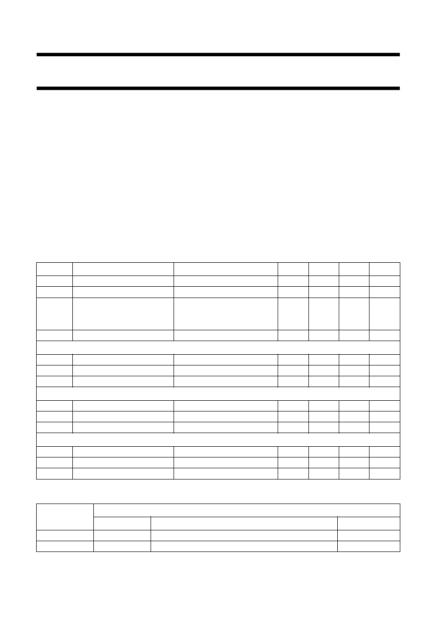
QUICK REFERENCE DATA
ORDERING INFORMATION
SYMBOL
PARAMETER
CONDITIONS
MIN.
TYP.
MAX.
TYP.
V
P
dynamic supply voltage
1.8
-
12
V
V
P
static supply voltage
2.1
-
12
V
I
P
supply current
AM mode
11.9
15.0
18.9
mA
FM mode
13.5
16.5
20.2
mA
T
amb
operating ambient temperature
-
15
-
+60
∞
C
AM performance
V
in1
RF sensitivity
40
55
70
µ
V
V
28
AF output voltage
36
45
70
mV
THD
total harmonic distortion
-
0.8
2.0
%
FM performance
V
in3
RF sensitivity
1.0
2.0
3.8
µ
V
V
28
AF output voltage
50
61
72
mV
THD
total harmonic distortion
-
0.3
0.8
%
MPX performance
cs
channel separation
26
30
-
dB
A
MPX
MPX voltage gain
V
AF-L
/V
in9
; S5 in position MONO
-
1.5
0
+1.0
dB
THD
total harmonic distortion
-
0.5
1.0
%
TYPE NUMBER
PACKAGE
NAME
DESCRIPTION
VERSION
TEA5711
SDIP32
plastic shrink dual in-line package; 32 leads (400 mil)
SOT232-1
TEA5711T
SO32
plastic small outline package; 32 leads; body width 7.5 mm
SOT287-1
September 1994
3
Philips Semiconductors
Product specification
AM/FM stereo radio circuit
TEA571
1; TEA571
1T
This text is here in white to force landscape pages to be rotated correctly when browsing through the pdf in the Acrobat reader.This text is here in
_
white to force landscape pages to be rotated correctly when browsing through the pdf in the Acrobat reader.This text is here inThis text is here in
white to force landscape pages to be rotated correctly when browsing through the pdf in the Acrobat reader. white to force landscape pages to be ...
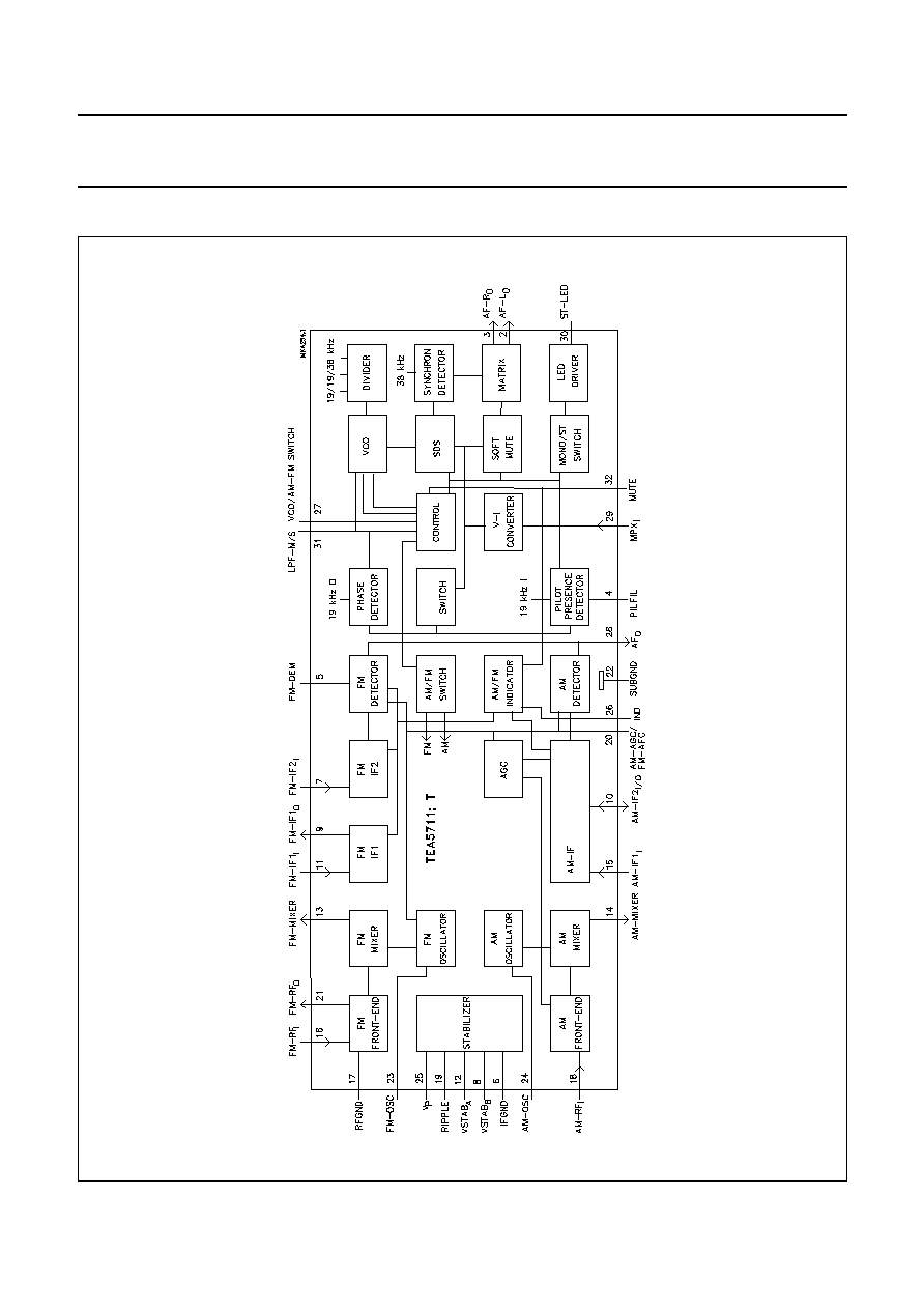
BLOCK DIAGRAM
Fig.1 Block diagram.

September 1994
4
Philips Semiconductors
Product specification
AM/FM stereo radio circuit
TEA5711; TEA5711T
PINNING
SYMBOL
PIN
DESCRIPTION
n.c.
1
not connected
AF-L
O
2
left channel audio output (output impedance typ. 4.3 k
)
AF-R
O
3
right channel audio output (output impedance typ. 4.3 k
)
PILFIL
4
pilot detector filter pin
FM-DEM
5
ceramic discriminator pin
IFGND
6
ground of IF, detector and MPX stages
FM-IF2
I
7
second FM-IF input (input impedance typ. 330
)
VSTAB
B
8
stabilized internal supply voltage (B)
FM-IF1
O
9
first FM-IF output (output impedance typ. 330
)
AM-IF2
I/O
10
input/output to IFT; output: current source
FM-IF1
I
11
first FM-IF input (input impedance typ. 330
)
VSTAB
A
12
stabilized internal supply voltage (A)
FM-MIXER
13
output to ceramic IF filter (output impedance typ. 330
)
AM-MIXER
14
open-collector output to IFT
AM-IF1
I
15
input from IFT or ceramic filter (input impedance typ. 3 k
)
FM-RF
I
16
FM-RF aerial input (input impedance typ. 50
)
RFGND
17
FM-RF ground
AM-RF
I
18
parallel tuned AM aerial circuit to ground (total input capacitance typ. 3 pF)
RIPPLE
19
ripple capacitor pin
AM-AGC/FM-AFC
20
AGC/AFC capacitor pin
FM-RF
O
21
parallel tuned FM-RF circuit to ground
SUBGND
22
substrate and RF ground
FM-OSC
23
parallel tuned FM-oscillator circuit to ground
AM-OSC
24
parallel tuned AM-oscillator circuit to ground
V
P
25
positive supply voltage
IND
26
signal level output
VCO/AM-FM SWITCH
27
VCO and switch terminal: open for AM; ground for FM
AF
O
28
AM/FM AF output (output impedance typ. 5 k
)
MPX
I
29
input for stereo decoder (input impedance typ. 180 k
)
ST-LED
30
stereo indicator
LPF-M/S
31
pin for loop-filter and mono/stereo switch
MUTE
32
mute pin

September 1994
5
Philips Semiconductors
Product specification
AM/FM stereo radio circuit
TEA5711; TEA5711T
Fig.2 Pin configuration; TEA5711.
Fig.3 Pin configuration; TEA5711T.
September 1994
6
Philips Semiconductors
Product specification
AM/FM stereo radio circuit
TEA5711; TEA5711T
FUNCTIONAL DESCRIPTION
The AM circuit incorporates a double balanced mixer, a
one pin low-voltage oscillator (up to 30 MHz) a
field-strength indicator output and is designed for
distributed selectivity.
The AM input is designed to be connected to the top of a
tuned circuit. AGC controls the IF amplification and for
large signals it lowers the input impedance.
The first AM selectivity can be an IFT as well as an IFT
combined with a ceramic filter; the second one is an IFT.
The FM circuit incorporates a tuned RF stage, a double
balanced mixer, a one-pin oscillator, a field-strength
indicator output and is designed for distributed IF ceramic
filters. The FM quadrature detector uses a ceramic
resonator.
The PLL stereo decoder incorporates a signal dependent
stereo circuit, a soft-mute circuit and a stereo indicator
LED driver.
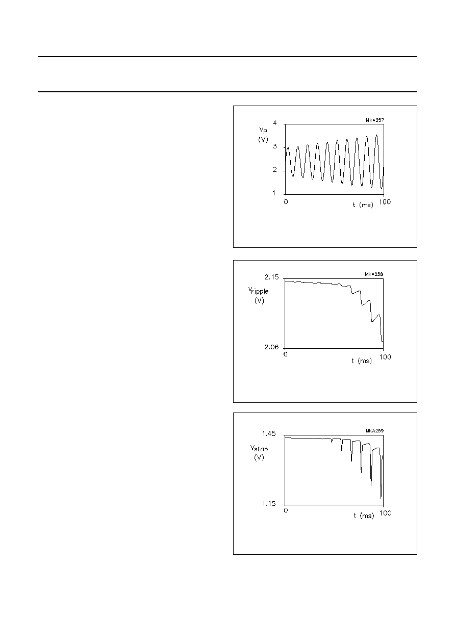
Supply voltage behaviour
The TEA5711 incorporates internal stabilized power
supplies. The maximum supply voltage is 12 V, the
minimum voltage can go down temporarily to 1.8 V without
any loss in performance.
Due to the capacitor at pin 19 (RIPPLE) the IC gives
excellent performance, even when the actual supply
voltage at pin 25 (V
P
) drops below the voltage at pin 19
(RIPPLE).
Figures 4, 5 and 6 show that V
stab
, which is dominant for
the overall IC performance, remains unaffected, even if V
P
drops down to 1.8 V or less. In this typical example the
static or average V
P
is equal to 2.5 V. Dips in V
stab
appear
only when the peak-to-peak value of the AC-component of
V
P
>
2 V, i.e. when the dynamic value of V
P
drops down to
1.5 V for a short moment.
Fig.4
Supply voltage behaviour; V
P
as a
function of time.
Fig.5
Supply voltage behaviour; V
ripple
as a
function of time.
BBBBBBBBBBBBBBBBBBBBBBBBBBBBBBBBBBBBBBBBBBBBBBBBBBBBB
BBBBBBBBBBBBBBBBBBBBBBBBBBBBBBBBBBBBBBBBBBBBBBBBBBBBB
BBBBBBBBBBBBBBBBBBBBBBBBBBBBBBBBBBBBBBBBBBBBBBBBBBBBB
BBBBBBBBBBBBBBBBBBBBBBBBBBBBBBBBBBBBBBBBBBBBBBBBBBBBB
BBBBBBBBBBBBBBBBBBBBBBBBBBBBBBBBBBBBBBBBBBBBBBBBBBBBB
BBBBBBBBBBBBBBBBBBBBBBBBBBBBBBBBBBBBBBBBBBBBBBBBBBBBB
BBBBBBBBBBBBBBBBBBBBBBBBBBBBBBBBBBBBBBBBBBBBBBBBBBBBB
BBBBBBBBBBBBBBBBBBBBBBBBBBBBBBBBBBBBBBBBBBBBBBBBBBBBB
BBBBBBBBBBBBBBBBBBBBBBBBBBBBBBBBBBBBBBBBBBBBBBBBBBBBB
BBBBBBBBBBBBBBBBBBBBBBBBBBBBBBBBBBBBBBBBBBBBBBBBBBBBB
BBBBBBBBBBBBBBBBBBBBBBBBBBBBBBBBBBBBBBBBBBBBBBBBBBBBB
BBBBBBBBBBBBBBBBBBBBBBBBBBBBBBBBBBBBBBBBBBBBBBBBBBBBB
BBBBBBBBBBBBBBBBBBBBBBBBBBBBBBBBBBBBBBBBBBBBBBBBBBBBB
BBBBBBBBBBBBBBBBBBBBBBBBBBBBBBBBBBBBBBBBBBBBBBBBBBBBB
BBBBBBBBBBBBBBBBBBBBBBBBBBBBBBBBBBBBBBBBBBBBBBBBBBBBB
BBBBBBBBBBBBBBBBBBBBBBBBBBBBBBBBBBBBBBBBBBBBBBBBBBBBB
BBBBBBBBBBBBBBBBBBBBBBBBBBBBBBBBBBBBBBBBBBBBBBBBBBBBB
BBBBBBBBBBBBBBBBBBBBBBBBBBBBBBBBBBBBBBBBBBBBBBBBBBBBB
BBBBBBBBBBBBBBBBBBBBBBBBBBBBBBBBBBBBBBBBBBBBBBBBBBBBB
BBBBBBBBBBBBBBBBBBBBBBBBBBBBBBBBBBBBBBBBBBBBBBBBBBBBB
BBBBBBBBBBBBBBBBBBBBBBBBBBBBBBBBBBBBBBBBBBBBBBBBBBBBB
BBBBBBBBBBBBBBBBBBBBBBBBBBBBBBBBBBBBBBBBBBBBBBBBBBBBB
BBBBBBBBBBBBBBBBBBBBBBBBBBBBBBBBBBBBBBBBBBBBBBBBBBBBB
BBBBBBBBBBBBBBBBBBBBBBBBBBBBBBBBBBBBBBBBBBBBBBBBBBBBB
BBBBBBBBBBBBBBBBBBBBBBBBBBBBBBBBBBBBBBBBBBBBBBBBBBBBB
BBBBBBBBBBBBBBBBBBBBBBBBBBBBBBBBBBBBBBBBBBBBBBBBBBBBB
BBBBBBBBBBBBBBBBBBBBBBBBBBBBBBBBBBBBBBBBBBBBBBBBBBBBB
BBBBBBBBBBBBBBBBBBBBBBBBBBBBBBBBBBBBBBBBBBBBBBBBBBBBB
BBBBBBBBBBBBBBBBBBBBBBBBBBBBBBBBBBBBBBBBBBBBBBBBBBBBB
BBBBBBBBBBBBBBBBBBBBBBBBBBBBBBBBBBBBBBBBBBBBBBBBBBBBB
BBBBBBBBBBBBBBBBBBBBBBBBBBBBBBBBBBBBBBBBBBBBBBBBBBBBB
BBBBBBBBBBBBBBBBBBBBBBBBBBBBBBBBBBBBBBBBBBBBBBBBBBBBB
BBBBBBBBBBBBBBBBBBBBBBBBBBBBBBBBBBBBBBBBBBBBBBBBBBBBB
BBBBBBBBBBBBBBBBBBBBBBBBBBBBBBBBBBBBBBBBBBBBBBBBBBBBB
BBBBBBBBBBBBBBBBBBBBBBBBBBBBBBBBBBBBBBBBBBBBBBBBBBBBB
BBBBBBBBBBBBBBBBBBBBBBBBBBBBBBBBBBBBBBBBBBBBBBBBBBBBB
BBBBBBBBBBBBBBBBBBBBBBBBBBBBBBBBBBBBBBBBBBBBBBBBBBBBB
Fig.6
Supply voltage behaviour; V
stab
as a
function of time.
BBBBBBBBBBBBBBBBBBBBBBBBBBBBBBBBBBBBBBBBBBBBBBBBBBBBB
BBBBBBBBBBBBBBBBBBBBBBBBBBBBBBBBBBBBBBBBBBBBBBBBBBBBB
BBBBBBBBBBBBBBBBBBBBBBBBBBBBBBBBBBBBBBBBBBBBBBBBBBBBB
BBBBBBBBBBBBBBBBBBBBBBBBBBBBBBBBBBBBBBBBBBBBBBBBBBBBB
BBBBBBBBBBBBBBBBBBBBBBBBBBBBBBBBBBBBBBBBBBBBBBBBBBBBB
BBBBBBBBBBBBBBBBBBBBBBBBBBBBBBBBBBBBBBBBBBBBBBBBBBBBB
BBBBBBBBBBBBBBBBBBBBBBBBBBBBBBBBBBBBBBBBBBBBBBBBBBBBB
BBBBBBBBBBBBBBBBBBBBBBBBBBBBBBBBBBBBBBBBBBBBBBBBBBBBB
BBBBBBBBBBBBBBBBBBBBBBBBBBBBBBBBBBBBBBBBBBBBBBBBBBBBB
BBBBBBBBBBBBBBBBBBBBBBBBBBBBBBBBBBBBBBBBBBBBBBBBBBBBB
BBBBBBBBBBBBBBBBBBBBBBBBBBBBBBBBBBBBBBBBBBBBBBBBBBBBB
BBBBBBBBBBBBBBBBBBBBBBBBBBBBBBBBBBBBBBBBBBBBBBBBBBBBB
BBBBBBBBBBBBBBBBBBBBBBBBBBBBBBBBBBBBBBBBBBBBBBBBBBBBB
BBBBBBBBBBBBBBBBBBBBBBBBBBBBBBBBBBBBBBBBBBBBBBBBBBBBB
BBBBBBBBBBBBBBBBBBBBBBBBBBBBBBBBBBBBBBBBBBBBBBBBBBBBB
BBBBBBBBBBBBBBBBBBBBBBBBBBBBBBBBBBBBBBBBBBBBBBBBBBBBB
BBBBBBBBBBBBBBBBBBBBBBBBBBBBBBBBBBBBBBBBBBBBBBBBBBBBB
BBBBBBBBBBBBBBBBBBBBBBBBBBBBBBBBBBBBBBBBBBBBBBBBBBBBB
BBBBBBBBBBBBBBBBBBBBBBBBBBBBBBBBBBBBBBBBBBBBBBBBBBBBB
BBBBBBBBBBBBBBBBBBBBBBBBBBBBBBBBBBBBBBBBBBBBBBBBBBBBB
BBBBBBBBBBBBBBBBBBBBBBBBBBBBBBBBBBBBBBBBBBBBBBBBBBBBB
BBBBBBBBBBBBBBBBBBBBBBBBBBBBBBBBBBBBBBBBBBBBBBBBBBBBB
BBBBBBBBBBBBBBBBBBBBBBBBBBBBBBBBBBBBBBBBBBBBBBBBBBBBB
BBBBBBBBBBBBBBBBBBBBBBBBBBBBBBBBBBBBBBBBBBBBBBBBBBBBB
BBBBBBBBBBBBBBBBBBBBBBBBBBBBBBBBBBBBBBBBBBBBBBBBBBBBB
BBBBBBBBBBBBBBBBBBBBBBBBBBBBBBBBBBBBBBBBBBBBBBBBBBBBB
BBBBBBBBBBBBBBBBBBBBBBBBBBBBBBBBBBBBBBBBBBBBBBBBBBBBB
BBBBBBBBBBBBBBBBBBBBBBBBBBBBBBBBBBBBBBBBBBBBBBBBBBBBB
BBBBBBBBBBBBBBBBBBBBBBBBBBBBBBBBBBBBBBBBBBBBBBBBBBBBB
BBBBBBBBBBBBBBBBBBBBBBBBBBBBBBBBBBBBBBBBBBBBBBBBBBBBB
BBBBBBBBBBBBBBBBBBBBBBBBBBBBBBBBBBBBBBBBBBBBBBBBBBBBB
BBBBBBBBBBBBBBBBBBBBBBBBBBBBBBBBBBBBBBBBBBBBBBBBBBBBB
BBBBBBBBBBBBBBBBBBBBBBBBBBBBBBBBBBBBBBBBBBBBBBBBBBBBB
BBBBBBBBBBBBBBBBBBBBBBBBBBBBBBBBBBBBBBBBBBBBBBBBBBBBB
BBBBBBBBBBBBBBBBBBBBBBBBBBBBBBBBBBBBBBBBBBBBBBBBBBBBB
BBBBBBBBBBBBBBBBBBBBBBBBBBBBBBBBBBBBBBBBBBBBBBBBBBBBB
BBBBBBBBBBBBBBBBBBBBBBBBBBBBBBBBBBBBBBBBBBBBBBBBBBBBB
September 1994
7
Philips Semiconductors
Product specification
AM/FM stereo radio circuit
TEA5711; TEA5711T
LIMITING VALUES
In accordance with the Absolute Maximum Rating System (IEC 134).
THERMAL CHARACTERISTICS
SYMBOL
PARAMETER
MIN.
MAX.
UNIT
V
P
supply voltage
0
12
V
T
stg
storage temperature
-
55
+150
∞
C
T
amb
operating ambient temperature
-
15
+60
∞
C
T
j
junction temperature
-
15
+150
∞
C
SYMBOL
PARAMETER
VALUE
UNIT
R
th j-a
thermal resistance from junction to ambient in free air
SDIP32
54
K/W
SO32
68
K/W
September 1994
8
Philips Semiconductors
Product specification
AM/FM stereo radio circuit
TEA5711; TEA5711T
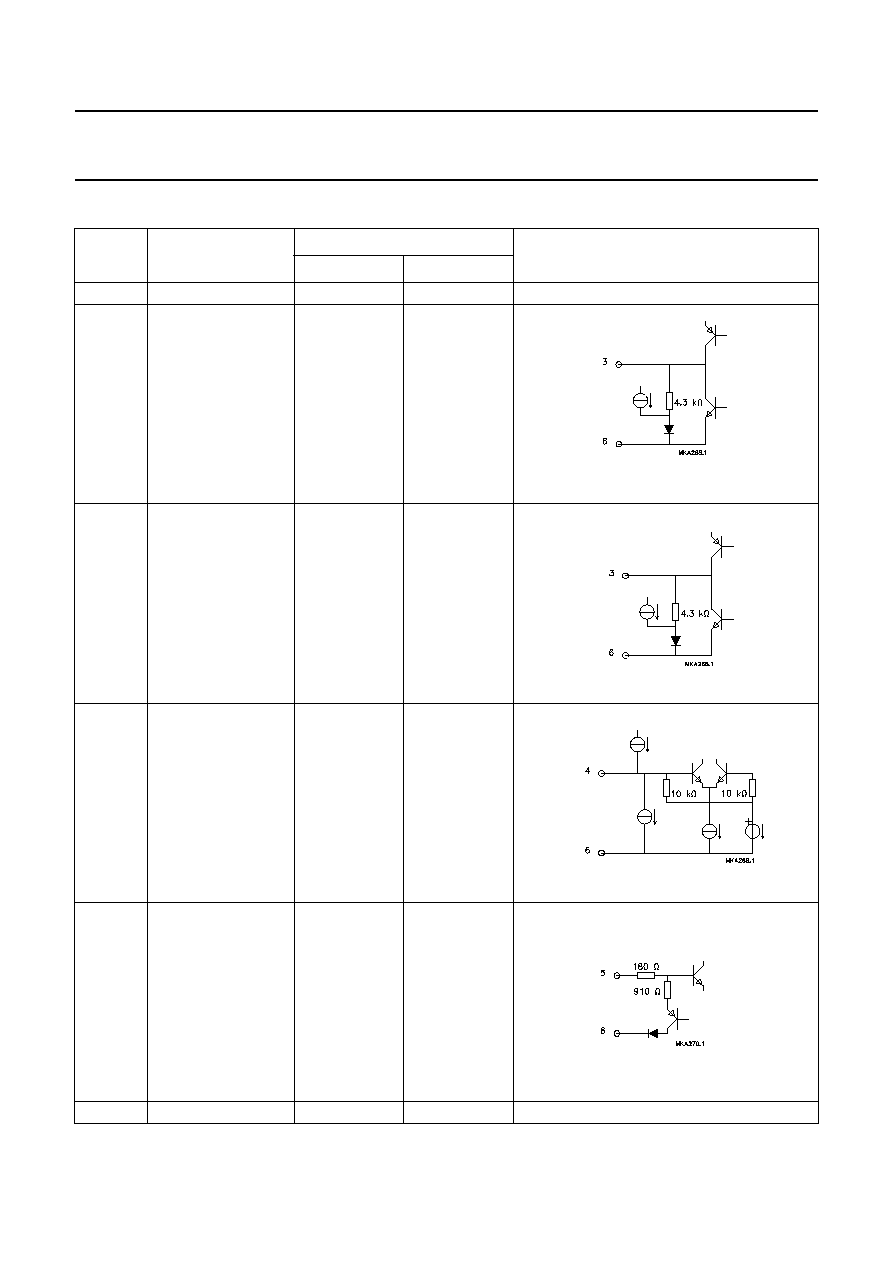
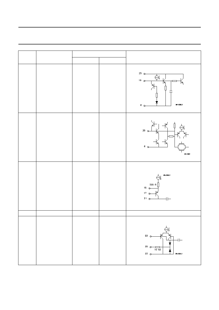
CIRCUIT DESIGN DATA
PIN NO.
PIN SYMBOL
DC PIN VOLTAGE (V)
EQUIVALENT CIRCUIT
AM
FM
1
n.c.
-
-
2
AF-L
O
output
0.65
0.65
3
AF-R
O
output
0.65
0.65
4
PILFIL
0.95
0.95
5
FM-DEM
-
1.0
6
IFGND
0
0
BB
BB
BB
BB
BB
BB
BB
BB
BB
BB
BB
BB
BB
BB
BBBB
BBBBBB
BB
BB
BB
September 1994
9
Philips Semiconductors
Product specification
AM/FM stereo radio circuit
TEA5711; TEA5711T
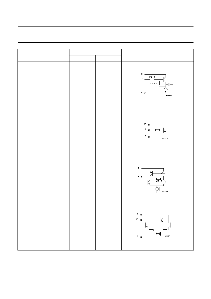
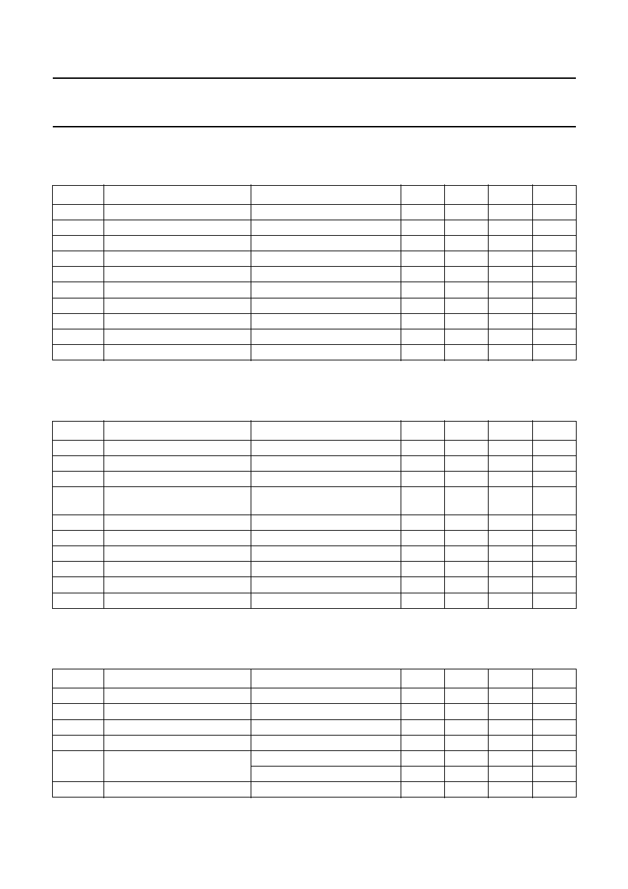
7
FM-IF2
I
input
-
0.73
8
VSTAB
B
1.4
1.4
9
FM-IF1
O
output
-
0.69
10
AM-IF2
I/O
input/output
1.4
1.4
PIN NO.
PIN SYMBOL
DC PIN VOLTAGE (V)
EQUIVALENT CIRCUIT
AM
FM
BBBB
BB
BB
BB
BBBB
BBBB
BBBB
BBBB
BBBB
BBBB
BBBB
September 1994
10
Philips Semiconductors
Product specification
AM/FM stereo radio circuit
TEA5711; TEA5711T
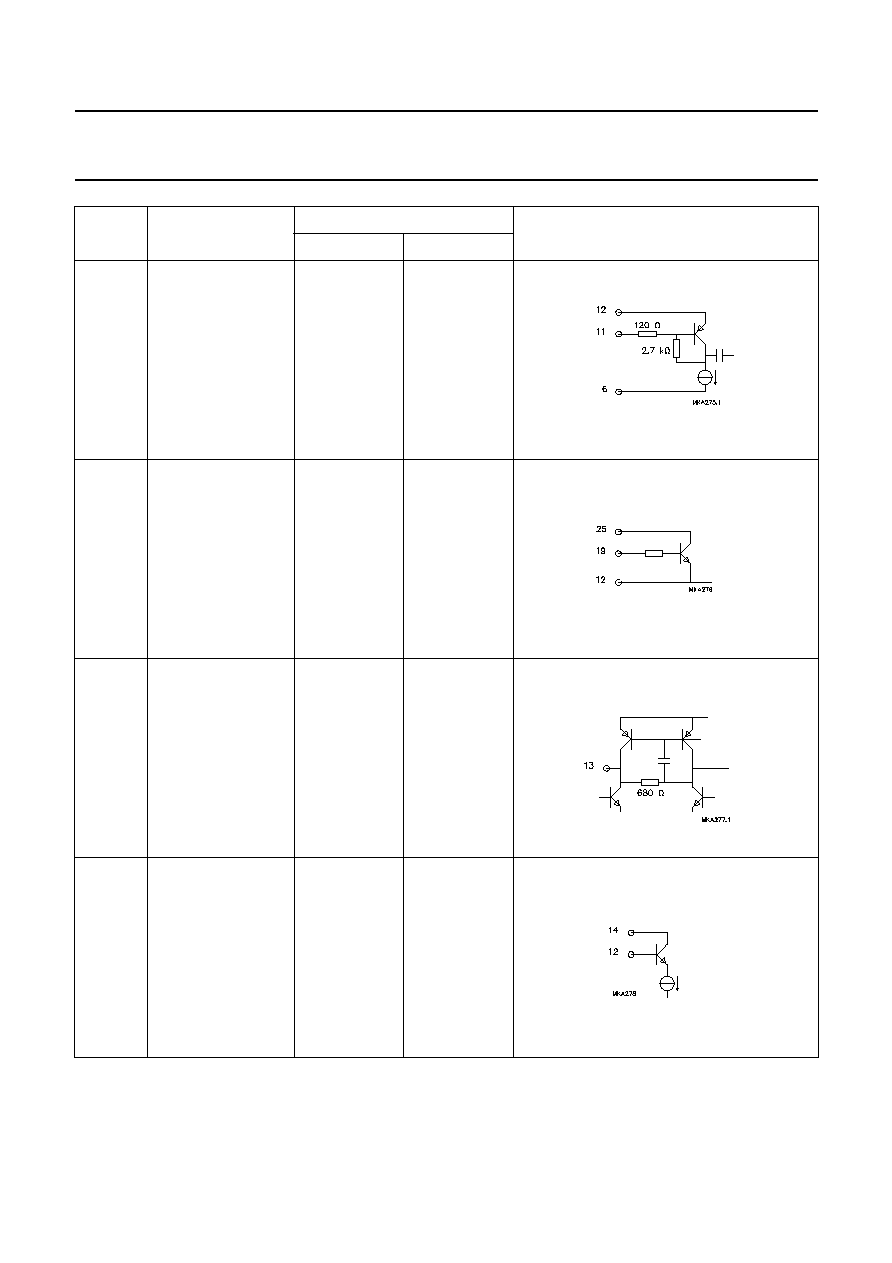
11
FM-IF1
I
input
-
0.73
12
VSTAB
A
1.4
1.4
13
FM-MIXER
output
-
1.0
14
AM-MIXER
output
1.4
1.4
PIN NO.
PIN SYMBOL
DC PIN VOLTAGE (V)
EQUIVALENT CIRCUIT
AM
FM
BB
BB
BB
BBBB
BBBB
BBBB
BBBB
BBBB
September 1994
11
Philips Semiconductors
Product specification
AM/FM stereo radio circuit
TEA5711; TEA5711T
15
AM-IF1
I
input
1.4
1.4
16
FM-RF
I
input
-
0.73
17
RFGND
0
0
18
AM-RF
I
input
0
0
PIN NO.
PIN SYMBOL
DC PIN VOLTAGE (V)
EQUIVALENT CIRCUIT
AM
FM
BBBB
BB
BB
BB
BBBB
BB
BB
BB
BB
BB
BB
BB
September 1994
12
Philips Semiconductors
Product specification
AM/FM stereo radio circuit
TEA5711; TEA5711T
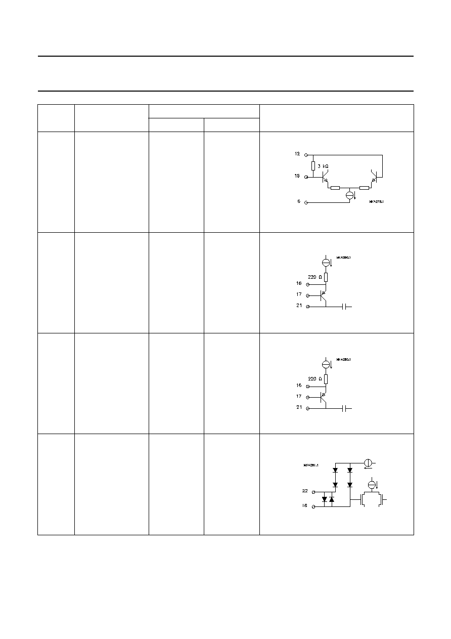
19
RIPPLE
2.1
2.1
20
AM-AGC/
FM-AFC
0.1
0.7
21
FM-RF
O
0
0
22
SUBGND
0
0
23
FM-OSC
0
0
PIN NO.
PIN SYMBOL
DC PIN VOLTAGE (V)
EQUIVALENT CIRCUIT
AM
FM
BB
BB
BB
BB
BB
BB
BBBB
BBBB
BB
BB
BB
BB
BB
BB
BB
BBBB
BBBB

September 1994
13
Philips Semiconductors
Product specification
AM/FM stereo radio circuit
TEA5711; TEA5711T
24
AM-OSC
0
0
25
V
P
3.0
3.0
26
IND
output
3.0
3.0
27
VCO and
AM/FM
switch
1.3
0.95
28
AF
output
0.6
0.7
PIN NO.
PIN SYMBOL
DC PIN VOLTAGE (V)
EQUIVALENT CIRCUIT
AM
FM
BB
BB
BB
BB
BB
BB
BB
BB
BB
BB
BB
BB
BBBB
BBBB

September 1994
14
Philips Semiconductors
Product specification
AM/FM stereo radio circuit
TEA5711; TEA5711T
29
MPX
input
1.23
1.23
30
ST-LED
3.0
3.0
31
LPF-M/S
0.1
0.8
32
MUTE
0.7
0.7
PIN NO.
PIN SYMBOL
DC PIN VOLTAGE (V)
EQUIVALENT CIRCUIT
AM
FM
BBBB
BB
BB
BB
BB
BB
BB
BB
BB
BB
BB
BBBB
BBBB
BB
BB
BB
BB
September 1994
15
Philips Semiconductors
Product specification
AM/FM stereo radio circuit
TEA5711; TEA5711T
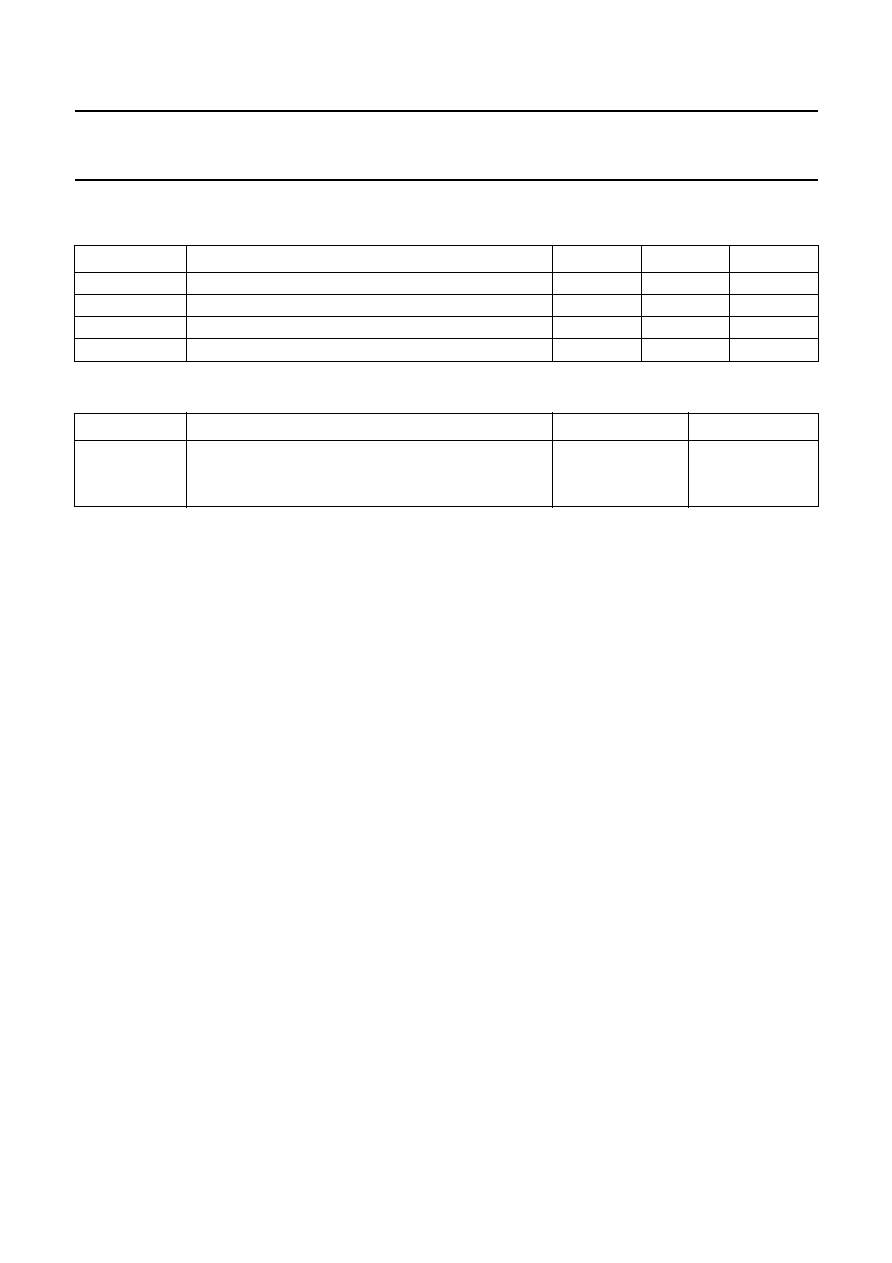
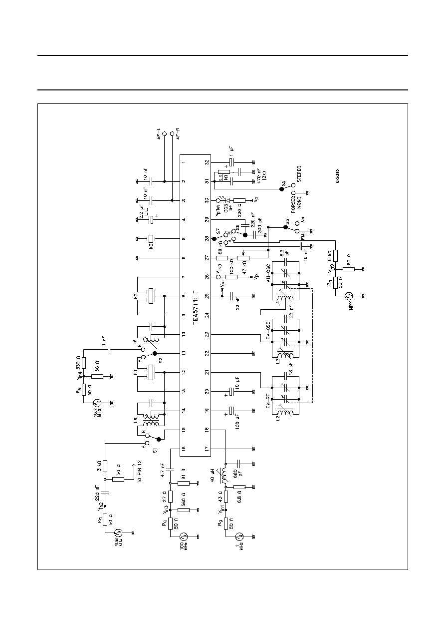
AM CHARACTERISTICS
f
i
= 1 MHz; m = 0.3; f
m
= 1 kHz; V
P
= 3.0 V; measured in Fig.7 with S1 in position B, S2 in position A and S7 in
position A; unless otherwise specified.
FM CHARACTERISTICS
f
i
= 100 MHz;
f = 22.5 kHz; f
m
= 1 kHz; V
P
= 3.0 V; measured in Fig.7 with S1 in position B, S2 in position A and S7 in
position A; unless otherwise specified.
STEREO DECODER CHARACTERISTICS
f
i
= 1 kHz; V
in9(L+R)
= 195 mv; pilot = 20 mV; V
P
= 3.0 V; measured in Fig.7 with S1 in position B, S2 in position A, S6 in
position A, S7 in position A and S5 in position STEREO; unless otherwise specified.
SYMBOL
PARAMETER
CONDITIONS
MIN.
TYP.
MAX.
UNIT
I
P
supply current
no input signal
11.9
15.0
18.9
mA
C
i
input capacitance
V
20
= 0.2 V
-
3
-
pF
G
c
front-end conversion gain
V
20
= 0.2 V
1.8
3.3
5.0
V
in1
RF sensitivity
S/N = 26 dB
40
55
70
µ
V
V
in2
IF sensitivity
V
28
= 30 mV; S1 in position A
0.13
0.2
0.45
mV
V
28
AF output voltage
V
in2
= 3.16 mV; S1 in position A
36
45
70
mV
THD
total harmonic distortion
V
in1
= 1 mV
-
0.8
2.0
%
V
in1
large signal handling
m = 0.8; THD
8%
150
300
-
mV
I
IND
indicator current
V
in2
= 100 mV; S1 in position A
120
170
230
µ
A
I
INDOFF
indicator OFF current
V
in2
= 0 V; S1 in position A
-
0
10
µ
A
SYMBOL
PARAMETER
CONDITIONS
MIN.
TYP.
MAX.
UNIT
I
P
supply current
no input signal
13.5
16.5
20.2
mA
V
in3
RF limiting sensitivity
V
28
=
-
3 dB
0.4
1.2
3.8
µ
V
V
in3
RF sensitivity
S/N = 26 dB
1.0
2.0
3.8
µ
V
V
11
/V
in3
front-end voltage gain
V
in3
1 mV;
including ceramic filter K1
12
18
22
dB
V
in4
IF sensitivity
S2 in position B; V
28
=
-
3 dB
-
20
30
µ
V
V
28
AF output voltage
V
in3
= 1 mV
50
61
72
mV
THD
total harmonic distortion
V
in3
= 1 mV;
f = 22.5 kHz
-
0.3
0.8
%
V
in3
large signal handling
THD
5%
-
500
-
mV
I
IND
indicator current
V
in4
= 100 mV; S2 in position B
190
255
320
µ
A
I
INDOFF
indicator OFF current
V
in4
= 0 V; S2 in position B
-
0
2
µ
A
SYMBOL
PARAMETER
CONDITIONS
MIN.
TYP.
MAX.
UNIT
A
MPX
MPX voltage gain V
AF-L
/V
in9
S5 in position MONO
-
1.5
0
+1.0
dB
THD
total harmonic distortion
-
0.5
1.0
%
(S+N)/N
signal plus noise-to-noise ratio
pilot = 20 mV
-
74
-
dB
cs
channel separation
L = 1; R = 0 or L = 0; R = 1
26
30
-
dB
SC
stereo control
V
in3
= 120
µ
V
-
30
-
dB
V
in3
= 10
µ
V
-
1
-
dB
MUTE
AF output signal suppression
V
in3
2
µ
V
-
20
-
dB
September 1994
16
Philips Semiconductors
Product specification
AM/FM stereo radio circuit
TEA571
1; TEA571
1T
This text is here in white to force landscape pages to be rotated correctly when browsing through the pdf in the Acrobat reader.This text is here in
_
white to force landscape pages to be rotated correctly when browsing through the pdf in the Acrobat reader.This text is here inThis text is here in
white to force landscape pages to be rotated correctly when browsing through the pdf in the Acrobat reader. white to force landscape pages to be ...
Fig.7 Test circuit.
c
c
cc
cc
c
c
September 1994
17
Philips Semiconductors
Product specification
AM/FM stereo radio circuit
TEA571
1; TEA571
1T
This text is here in white to force landscape pages to be rotated correctly when browsing through the pdf in the Acrobat reader.This text is here in
_
white to force landscape pages to be rotated correctly when browsing through the pdf in the Acrobat reader.This text is here inThis text is here in
white to force landscape pages to be rotated correctly when browsing through the pdf in the Acrobat reader. white to force landscape pages to be ...
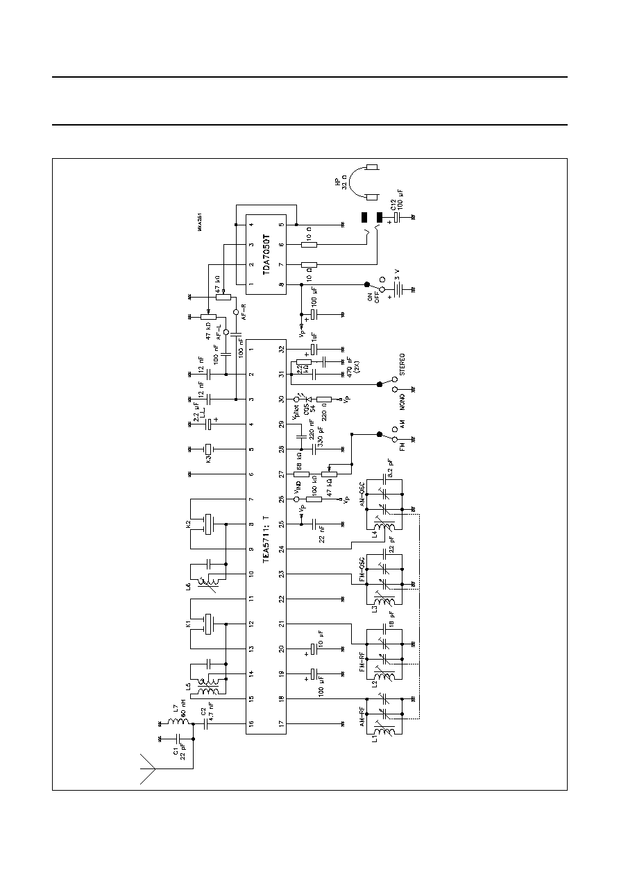
APPLICA
TION INFORMA
TION
Fig.8 Application circuit of TEA5711 (AM: 522 to 1611 kHz, FM: 87.5 to 108 MHz) with stereo headphone amplifier TDA7050T.

September 1994
18
Philips Semiconductors
Product specification
AM/FM stereo radio circuit
TEA5711; TEA5711T
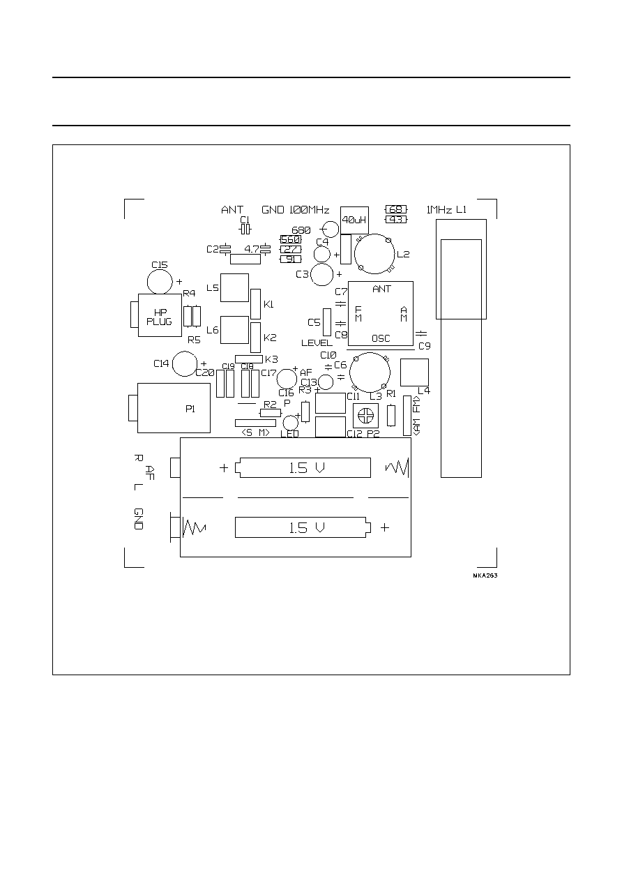
Fig.9 Printed-circuit board layout (track side) for application circuit of Fig.8.
September 1994
19
Philips Semiconductors
Product specification
AM/FM stereo radio circuit
TEA5711; TEA5711T
Fig.10 Printed-circuit board layout (component side) for application circuit of Fig.8.
September 1994
20
Philips Semiconductors
Product specification
AM/FM stereo radio circuit
TEA5711; TEA5711T
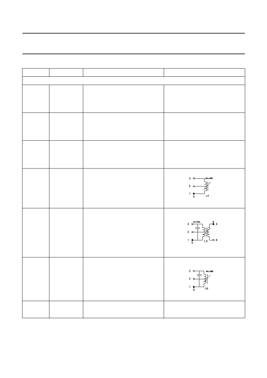
Components for Figs 7 and 8
NUMBER
TYPE
DESCRIPTION
CIRCUIT
Coils
L1
AM-AERIAL
ferroceptor
length = 6 cm
L1-2 = 625
µ
H
N1-2 = 105 turns
unloaded Q
L2
FM-RF
L1-2 = 66 nH
N1-2 = 2.5 turns
unloaded Q = 150T
TOKO type S18
TOKO number 301SS-0200
L3
FM-OSC
L1-2 = 40 nH
N1-2 = 1.5 turns
unloaded Q = 150
TOKO type S18
TOKO number 301SS-0100
L4
AM-OSC
L1-3 = 270
µ
H
N1-2 = 18
N2-3 = 70
unloaded Q = 100
wire diameter 0.07 mm
TOKO type 7P
material TOKO 7BRS
L5
AM-IF1
L1-3 = 625
µ
H
N1-2 = 17 turns
N2-3 = 141 turns
N4-6 = 10 turns
C1-3 = 180 pF
unloaded Q = 90
wire diameter 0.07 mm
TOKO type 7P
material TOKO 7MCS
L6
AM-IF2
L1-3 = 625
µ
H
N1-2 = 28 turns
N2-3 = 130 turns
C1-3 = 180 pF
unloaded Q = 90
wire diameter 0.07 mm
TOKO type 7P
material TOKO 7MCS
L7
FM-AERIAL
printcoil
L1-2 = 60 nH
N1-2 = 2.5 turns
September 1994
21
Philips Semiconductors
Product specification
AM/FM stereo radio circuit
TEA5711; TEA5711T
Application remarks
∑
Short circuiting: all pins are short-circuit proof except pin 16 (FM-RF
I
) with respect to the supply voltage pin.
∑
For an example of printed-circuit board layout: see Figs 9 and 10.
∑
Align VCO with aerial signal present.
L8
AM-RF
test circuit only:
L1-3 = 40
µ
H
N1-3 = 34 turns
unloaded Q = 85
wire diameter 0.09 mm
TOKO type 7P
material TOKO 7BRS
Ceramic filters
K1
FM-IF1
Murata SFE 10.7 MS 2
K2
FM-IF2
Murata SFE 10.7 MS 2
K3
FM-DET
Murata CDA 10.7 MC 40
Capacitors
C1
VARICON
AM: 140/82 pF
FM: 2
◊
20 pF
trimmer: 4
◊
8 pF
TOKO type number HU-22124
NUMBER
TYPE
DESCRIPTION
CIRCUIT
BBBBBBB
BBBBBBB
BBBBBBB
BBBBBBB
BBBBBBB
BBBBBBB
BBBBBB
BBBBBB
BBBBBB
BBBBBB
BBBBBB
BBBBBB
BBBBBB
BBBBBB
BBBBBB
BBBBBB
BBBBBB
BBBBBB
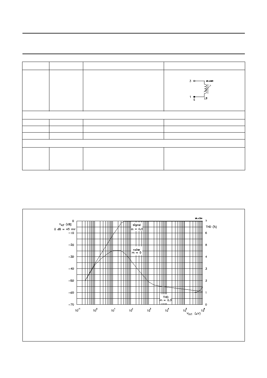
Fig.11 Typical AM audio voltage (V
AF
; signal at m = 0.3), noise and THD as a function of RF input
voltage (V
in1
; f
i
= 1 kHz). Measured in test circuit Fig.7 with V
P
= 3.0 V.
September 1994
22
Philips Semiconductors
Product specification
AM/FM stereo radio circuit
TEA5711; TEA5711T
BBBBBB
BBBBBB
BBBBBB
BBBBBB
BBBBBB
BBBBBB
BBBBBB
BBBBBB
BBBBBB
BBBBBB
BBBBBBB
BBBBBBB
BBBBBBB
BBBBBBB
BBBBBBB
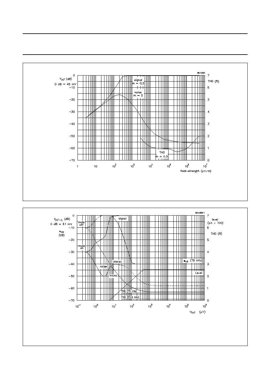
Fig.12 Typical AM audio voltage (V
AF
; signal at m = 0.3), noise and THD as a function of field-strength (f
i
= 1 kHz).
Measured in application circuit Fig.8 with V
P
= 3.0 V.
BBBBBBB
BBBBBBB
BBBBBBB
BBBBBB
BBBBBB
BBBBBB
BBBBBBBBBB
BBBBBBBBBB
BBBBBBBBBBBBBBBBB
BBBBBBBBBBBBBBBBB
BBBBBBBBBBBBBBBBB
BBBBBB
BBBBBB
BBBBBB
BBBB
BBBB
BBBB
BBBBB
BBBBB
BBBBB
BBBBB
BBBBB
BBBBB
BBBBB
BBBBB
BBBBB
BBBBB
BBBBB
BBBBB
BBBBB
BBBBB
BBBBB
BBBBB
BBBBB
BBBBB
BBBBBBBBBB
BBBBBBBBBB
BBBBBBBBBB
BBBB
BBBB
BBBB
BBBB
BBBB
BBBB
BBBB
BBBB
BBBB
Fig.13 Typical FM audio voltage (V
AF
; signal), noise, THD (at
f = 22.5 kHz and
f = 75 kHz) and indicator
current (level) as a function of RF input voltage (V
in1
;
f = 22.5 kHz). Curves are shown without
mute (mono) and with mute (mono and stereo). Channel separation at
f = 75 kHz. Measured in
test circuit Fig.7 with V
P
= 3.0 V.
September 1994
23
Philips Semiconductors
Product specification
AM/FM stereo radio circuit
TEA5711; TEA5711T
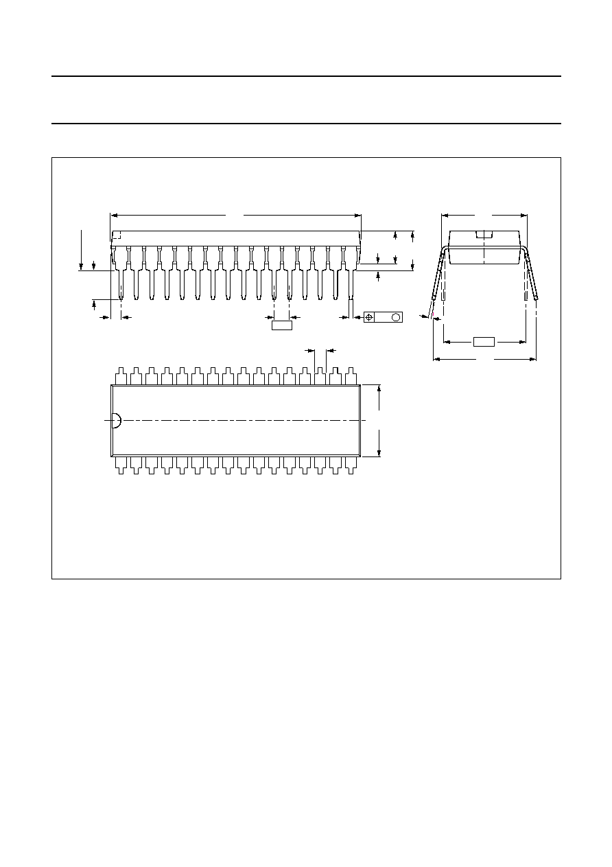
PACKAGE OUTLINES
Fig.14 Plastic shrink dual in-line package; 32 leads (400 mil); (SDIP32; SOT232-1).
17
16
1.3 max
9.1
8.7
29.4
28.5
3.8
max
4.7
max
0.51
min
0.18
M
0.53
max
1.778
(15x)
3.2
2.8
seating plane
1.6
max
10.7
10.2
0.32 max
10.16
12.2
10.5
MSA270
32
1
Dimensions in mm.
September 1994
24
Philips Semiconductors
Product specification
AM/FM stereo radio circuit
TEA5711; TEA5711T
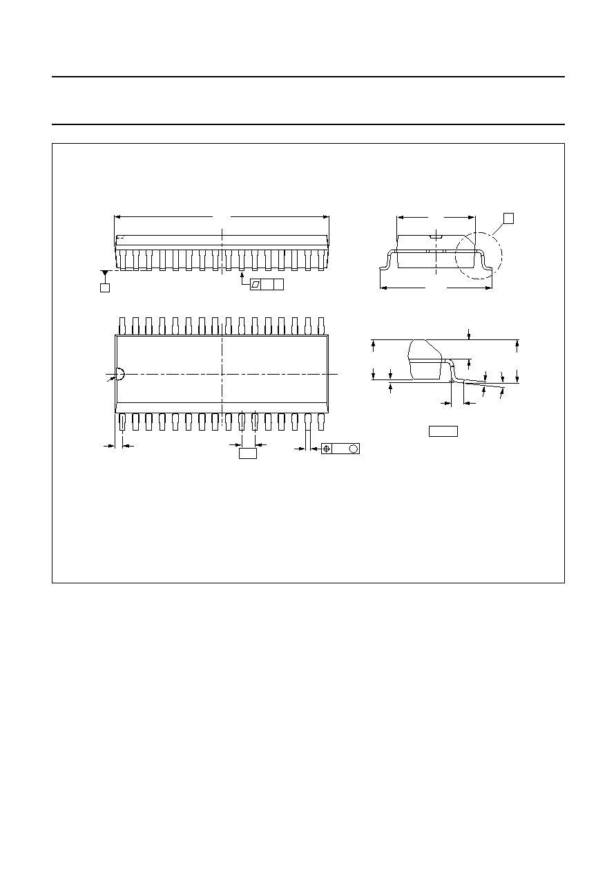
Fig.15 Plastic small outline package; 32 leads; body width 7.5 mm (SO32; SOT287-1).
Dimensions in mm.
S
0.1 S
0.27
0.18
0.3
0.1
2.45
2.25
1.2
1.0
2.65
2.35
detail A
10.65
10.0
A
MSA235 - 2
7.6
7.4
1.27
0.49
0.36
1
16
17
32
0.25
M
(32x)
pin 1
index
20.7
20.3
0.95
0.55
(4x)
0 to 8
o
1.1
0.5

September 1994
25
Philips Semiconductors
Product specification
AM/FM stereo radio circuit
TEA5711; TEA5711T
SOLDERING
Plastic dual in-line packages
B
Y DIP OR WAVE
The maximum permissible temperature of the solder is
260
∞
C; this temperature must not be in contact with the
joint for more than 5 s. The total contact time of successive
solder waves must not exceed 5 s.
The device may be mounted up to the seating plane, but
the temperature of the plastic body must not exceed the
specified storage maximum. If the printed-circuit board has
been pre-heated, forced cooling may be necessary
immediately after soldering to keep the temperature within
the permissible limit.
R
EPAIRING SOLDERED JOINTS
Apply the soldering iron below the seating plane (or not
more than 2 mm above it). If its temperature is below
300
∞
C, it must not be in contact for more than 10 s; if
between 300 and 400
∞
C, for not more than 5 s.
Plastic small-outline packages
B
Y WAVE
During placement and before soldering, the component
must be fixed with a droplet of adhesive. After curing the
adhesive, the component can be soldered. The adhesive
can be applied by screen printing, pin transfer or syringe
dispensing.
Maximum permissible solder temperature is 260
∞
C, and
maximum duration of package immersion in solder bath is
10 s, if allowed to cool to less than 150
∞
C within 6 s.
Typical dwell time is 4 s at 250
∞
C.
A modified wave soldering technique is recommended
using two solder waves (dual-wave), in which a turbulent
wave with high upward pressure is followed by a smooth
laminar wave. Using a mildly-activated flux eliminates the
need for removal of corrosive residues in most
applications.
B
Y SOLDER PASTE REFLOW
Reflow soldering requires the solder paste (a suspension
of fine solder particles, flux and binding agent) to be
applied to the substrate by screen printing, stencilling or
pressure-syringe dispensing before device placement.
Several techniques exist for reflowing; for example,
thermal conduction by heated belt, infrared, and
vapour-phase reflow. Dwell times vary between 50 and
300 s according to method. Typical reflow temperatures
range from 215 to 250
∞
C.
Preheating is necessary to dry the paste and evaporate
the binding agent. Preheating duration: 45 min. at 45
∞
C.
R
EPAIRING SOLDERED JOINTS
(
BY HAND
-
HELD SOLDERING
IRON OR PULSE
-
HEATED SOLDER TOOL
)
Fix the component by first soldering two, diagonally
opposite, end pins. Apply the heating tool to the flat part of
the pin only. Contact time must be limited to 10 s at up to
300
∞
C. When using proper tools, all other pins can be
soldered in one operation within 2 to 5 s at between 270
and 320
∞
C. (Pulse-heated soldering is not recommended
for SO packages.)
For pulse-heated solder tool (resistance) soldering of VSO
packages, solder is applied to the substrate by dipping or
by an extra thick tin/lead plating before package
placement.

September 1994
26
Philips Semiconductors
Product specification
AM/FM stereo radio circuit
TEA5711; TEA5711T
DEFINITIONS
LIFE SUPPORT APPLICATIONS
These products are not designed for use in life support appliances, devices, or systems where malfunction of these
products can reasonably be expected to result in personal injury. Philips customers using or selling these products for
use in such applications do so at their own risk and agree to fully indemnify Philips for any damages resulting from such
improper use or sale.
Data sheet status
Objective specification
This data sheet contains target or goal specifications for product development.
Preliminary specification
This data sheet contains preliminary data; supplementary data may be published later.
Product specification
This data sheet contains final product specifications.
Limiting values
Limiting values given are in accordance with the Absolute Maximum Rating System (IEC 134). Stress above one or
more of the limiting values may cause permanent damage to the device. These are stress ratings only and operation
of the device at these or at any other conditions above those given in the Characteristics sections of the specification
is not implied. Exposure to limiting values for extended periods may affect device reliability.
Application information
Where application information is given, it is advisory and does not form part of the specification.

September 1994
27
Philips Semiconductors
Product specification
AM/FM stereo radio circuit
TEA5711; TEA5711T
NOTES

Philips Semiconductors
Philips Semiconductors ≠ a worldwide company
Argentina: IEROD, Av. Juramento 1992 - 14.b, (1428)
BUENOS AIRES, Tel. (541)786 7633, Fax. (541)786 9367
Australia: 34 Waterloo Road, NORTH RYDE, NSW 2113,
Tel. (02)805 4455, Fax. (02)805 4466
Austria: Triester Str. 64, A-1101 WIEN, P.O. Box 213,
Tel. (01)60 101-1236, Fax. (01)60 101-1211
Belgium: Postbus 90050, 5600 PB EINDHOVEN, The Netherlands,
Tel. (31)40 783 749, Fax. (31)40 788 399
Brazil: Rua do Rocio 220 - 5
th
floor, Suite 51,
CEP: 04552-903-S√O PAULO-SP, Brazil.
P.O. Box 7383 (01064-970).
Tel. (011)821-2333, Fax. (011)829-1849
Canada: PHILIPS SEMICONDUCTORS/COMPONENTS:
Tel. (800) 234-7381, Fax. (708) 296-8556
Chile: Av. Santa Maria 0760, SANTIAGO,
Tel. (02)773 816, Fax. (02)777 6730
Colombia: IPRELENSO LTDA, Carrera 21 No. 56-17,
77621 BOGOTA, Tel. (571)249 7624/(571)217 4609,
Fax. (571)217 4549
Denmark: Prags Boulevard 80, PB 1919, DK-2300 COPENHAGEN S,
Tel. (032)88 2636, Fax. (031)57 1949
Finland: Sinikalliontie 3, FIN-02630 ESPOO,
Tel. (9)0-50261, Fax. (9)0-520971
France: 4 Rue du Port-aux-Vins, BP317,
92156 SURESNES Cedex,
Tel. (01)4099 6161, Fax. (01)4099 6427
Germany: P.O. Box 10 63 23, 20043 HAMBURG,
Tel. (040)3296-0, Fax. (040)3296 213.
Greece: No. 15, 25th March Street, GR 17778 TAVROS,
Tel. (01)4894 339/4894 911, Fax. (01)4814 240
Hong Kong: PHILIPS HONG KONG Ltd., 6/F Philips Ind. Bldg.,
24-28 Kung Yip St., KWAI CHUNG, N.T.,
Tel. (852)424 5121, Fax. (852)428 6729
India: Philips INDIA Ltd, Shivsagar Estate, A Block ,
Dr. Annie Besant Rd. Worli, Bombay 400 018
Tel. (022)4938 541, Fax. (022)4938 722
Indonesia: Philips House, Jalan H.R. Rasuna Said Kav. 3-4,
P.O. Box 4252, JAKARTA 12950,
Tel. (021)5201 122, Fax. (021)5205 189
Ireland: Newstead, Clonskeagh, DUBLIN 14,
Tel. (01)640 000, Fax. (01)640 200
Italy: PHILIPS SEMICONDUCTORS S.r.l.,
Piazza IV Novembre 3, 20124 MILANO,
Tel. (0039)2 6752 2531, Fax. (0039)2 6752 2557
Japan: Philips Bldg 13-37, Kohnan 2 -chome, Minato-ku, TOKYO 108,
Tel. (03)3740 5028, Fax. (03)3740 0580
Korea: (Republic of) Philips House, 260-199 Itaewon-dong,
Yongsan-ku, SEOUL, Tel. (02)794-5011, Fax. (02)798-8022
Malaysia: No. 76 Jalan Universiti, 46200 PETALING JAYA,
SELANGOR, Tel. (03)750 5214, Fax. (03)757 4880
Mexico: 5900 Gateway East, Suite 200, EL PASO, TX 79905,
Tel. 9-5(800)234-7381, Fax. (708)296-8556
Netherlands: Postbus 90050, 5600 PB EINDHOVEN, Bldg. VB
Tel. (040)783749, Fax. (040)788399
New Zealand: 2 Wagener Place, C.P.O. Box 1041, AUCKLAND,
Tel. (09)849-4160, Fax. (09)849-7811
Norway: Box 1, Manglerud 0612, OSLO,
Tel. (022)74 8000, Fax. (022)74 8341
Pakistan: Philips Electrical Industries of Pakistan Ltd.,
Exchange Bldg. ST-2/A, Block 9, KDA Scheme 5, Clifton,
KARACHI 75600, Tel. (021)587 4641-49,
Fax. (021)577035/5874546.
Philippines: PHILIPS SEMICONDUCTORS PHILIPPINES Inc,
106 Valero St. Salcedo Village, P.O. Box 2108 MCC, MAKATI,
Metro MANILA, Tel. (02)810 0161, Fax. (02)817 3474
Portugal: PHILIPS PORTUGUESA, S.A.,
Rua dr. AntÛnio Loureiro Borges 5, Arquiparque - Miraflores,
Apartado 300, 2795 LINDA-A-VELHA,
Tel. (01)4163160/4163333, Fax. (01)4163174/4163366.
Singapore: Lorong 1, Toa Payoh, SINGAPORE 1231,
Tel. (65)350 2000, Fax. (65)251 6500
South Africa: S.A. PHILIPS Pty Ltd.,
195-215 Main Road Martindale, 2092 JOHANNESBURG,
P.O. Box 7430 Johannesburg 2000,
Tel. (011)470-5911, Fax. (011)470-5494.
Spain: Balmes 22, 08007 BARCELONA,
Tel. (03)301 6312, Fax. (03)301 42 43
Sweden: Kottbygatan 7, Akalla. S-164 85 STOCKHOLM,
Tel. (0)8-632 2000, Fax. (0)8-632 2745
Switzerland: Allmendstrasse 140, CH-8027 ZÐRICH,
Tel. (01)488 2211, Fax. (01)481 77 30
Taiwan: PHILIPS TAIWAN Ltd., 23-30F, 66, Chung Hsiao West
Road, Sec. 1. Taipeh, Taiwan ROC, P.O. Box 22978,
TAIPEI 100, Tel. (02)388 7666, Fax. (02)382 4382.
Thailand: PHILIPS ELECTRONICS (THAILAND) Ltd.,
209/2 Sanpavuth-Bangna Road Prakanong,
Bangkok 10260, THAILAND,
Tel. (662)398-0141, Fax. (662)398-3319.
Turkey: Talatpasa Cad. No. 5, 80640 GÐLTEPE/ISTANBUL,
Tel. (0 212)279 2770, Fax. (0212)269 3094
United Kingdom: Philips Semiconductors LTD.,
276 Bath road, Hayes, MIDDLESEX UB3 5BX,
Tel. (081)73050000, Fax. (081)7548421
United States: 811 East Arques Avenue, SUNNYVALE,
CA 94088-3409, Tel. (800)234-7381, Fax. (708)296-8556
Uruguay: Coronel Mora 433, MONTEVIDEO,
Tel. (02)70-4044, Fax. (02)92 0601
For all other countries apply to: Philips Semiconductors,
International Marketing and Sales, Building BE-p,
P.O. Box 218, 5600 MD, EINDHOVEN, The Netherlands,
Telex 35000 phtcnl, Fax. +31-40-724825
SCD35
© Philips Electronics N.V. 1994
All rights are reserved. Reproduction in whole or in part is prohibited without the
prior written consent of the copyright owner.
The information presented in this document does not form part of any quotation
or contract, is believed to be accurate and reliable and may be changed without
notice. No liability will be accepted by the publisher for any consequence of its
use. Publication thereof does not convey nor imply any license under patent- or
other industrial or intellectual property rights.
Printed in The Netherlands