 | –≠–ª–µ–∫—Ç—Ä–æ–Ω–Ω—ã–π –∫–æ–º–ø–æ–Ω–µ–Ω—Ç: TEA5764HN | –°–∫–∞—á–∞—Ç—å:  PDF PDF  ZIP ZIP |

1.
General description
The TEA5764HN is a single chip electronically tuned FM stereo radio with Radio Data
System (RDS) and Radio Broadcast Data System (RBDS) demodulator and RDS/RBDS
decoder for portable application with fully integrated IF selectivity and demodulation.
The radio is completely adjustment free and only requires a minimum of small and low
cost external components.
The radio can tune to the European, US and Japanese FM bands. It has a low power
consumption and can operate at a low supply voltage.
2.
Features
s
High sensitivity due to integrated low noise RF input amplifier
s
FM mixer for conversion of the US/Europe (87.5 MHz to 108 MHz) and Japanese FM
band (76 MHz to 90 MHz) to IF
s
Preset tuning to receive Japanese TV audio up to 108 MHz
s
Auto search tuning, raster 100 kHz
s
RF automatic gain control circuit
s
LC tuner oscillator operating with low cost fixed chip inductors
s
Fully integrated FM IF selectivity
s
Fully integrated FM demodulator;
s
no external discriminator
s
Crystal oscillator at 32768 Hz, or external reference frequency at 32768 Hz
s
PLL synthesizer tuning system
s
IF counter; 7-bit output via the I
2
C-bus
s
Level detector; 4-bit level information output via the I
2
C-bus
s
Soft mute: signal dependent mute function
s
Mono/stereo blend: gradual change from mono to stereo, depending on signal
s
Adjustment-free stereo decoder
s
Autonomous search tuning function
s
Standby mode
s
MPX output
s
One software programmable port
s
Fully integrated RDS/RBDS demodulator in accordance with EN50067
s
RDS/RBDS decoder with memory for two RDS data blocks provides block
synchronization and error correction; block data and status information are available
via the I
2
C-bus
s
Audio pause detector
TEA5764HN
FM radio + RDS
Rev. 02 -- 9 August 2005
Product data sheet

TEA5764HN_2
© Koninklijke Philips Electronics N.V. 2005. All rights reserved.
Product data sheet
Rev. 02 -- 9 August 2005
2 of 64
Philips Semiconductors
TEA5764HN
FM radio + RDS
s
Interrupt flag
3.
Applications
s
FM stereo radio
4.
Quick reference data
Table 1:
Electrical parameters general
The listed parameters are valid when a crystal is used that meets the requirements as stated in
Table 47
; All RF input values
are defined in potential difference, except when EMF is explicitly stated.
Symbol
Parameter
Conditions
Min
Typ
Max
Unit
Supplies
V
CCA
analog supply voltage
2.5
2.7
3.3
V
I
CCA
analog supply current
V
CCA
= 2.5 V to 3.3 V
operating mode
12
13.7
16
mA
Standby mode
0
0.1
1
µ
A
V
CCD
digital supply voltage
2.5
2.7
3.3
V
I
CCD
digital supply current
V
CCD
= 2.5 V to 3.3 V
operating mode
0.3
0.7
1.5
mA
Standby mode
1
15
22.5
µ
A
Reference voltage
V
VREFDIG
digital reference voltage
for I
2
C-bus interface
1.65
1.8
V
CCD
V
I
VREFDIG
digital reference supply
current
operating mode;
V
VREFDIG
= 1.65 V to V
CCD
0
0.5
1
µ
A
General
f
i(FM)
FM input frequency
76
-
108
MHz
T
amb
ambient temperature
-
40
-
+85
∞
C
FM and RDS overall system parameters
V
sens(EMF)
sensitivity EMF value
voltage
f
RF
= 76 MHz to 108 MHz;
f = 22.5 kHz; f
mod
= 1 kHz;
(S+N)/N = 26 dB; TC
deem
= 75
µ
s;
A-weighting filter;
B
aud
= 300 Hz to 15 kHz
-
2.3
3.5
µ
V
IP3
in
in-band 3rd-order
intercept point
f
1
= 200 kHz;
f
2
= 400 kHz;
f
tune
= 76 MHz to 108 MHz;
RF
agc
= off
78
87
-
dB
µ
V
IP3
out
out-of-band 3rd-order
intercept point
f
1
= 4 MHz;
f
2
= 8 MHz;
f
tune
= 76 MHz to 108 MHz;
RF
agc
= off
87
93
-
dB
µ
V
S
selectivity
f
tune
= 76 MHz to 108 MHz
[1]
high-side;
f = +200 kHz
39
43
-
dB
low-side;
f =
-
200 kHz
32
36
-
dB
V
VAFL
left audio output voltage
on pin VAFL
V
RF
= 1 mV; L = R;
f = 22.5 kHz;
f
mod
= 1 kHz; no pre-emphasis;
TC
deem
= 75
µ
s
55
66
75
mV

TEA5764HN_2
© Koninklijke Philips Electronics N.V. 2005. All rights reserved.
Product data sheet
Rev. 02 -- 9 August 2005
3 of 64
Philips Semiconductors
TEA5764HN
FM radio + RDS
[1]
Low-side and high-side selectivity can be measured by changing the mixer LO injection from high-side to low-side.
5.
Ordering information
V
VAFR
right audio output voltage
on pin VAFR
V
RF
= 1 mV; L = R;
f = 22.5 kHz;
f
mod
= 1 kHz; no pre-emphasis;
TC
deem
= 75
µ
s
55
66
75
mV
(S+N)/N(m)
maximum signal-to-noise
ratio, mono
V
RF
= 1 mV;
f = 22.5 kHz; L = R;
f
mod
= 1 kHz; de-emphasis = 75
µ
s;
B
AF
= 300 Hz to 15 kHz; A-weighting
filter
54
57
-
dB
(S+N)/N(s)
maximum signal-to-noise
ratio, stereo
V
RF
= 1 mV;
f = 67.5 kHz; L = R;
f
mod
= 1 kHz;
f
pilot
= 6.75 kHz;
de-emphasis = 75
µ
s; B
AF
= 300 Hz
to 15 kHz; A-weighting filter
50
54
-
dB
cs
channel separation
MST = 0; R = 1 and L = 0 or R = 0
and L = 1; V
RF
= 30
µ
V; increasing
RF input level
27
33
-
dB
THD
total harmonic distortion
V
RF
= 1 mV;
f = 75 kHz;
f
mod
= 1 kHz; DTC = 0; B
aud
= 300 Hz
to 15 kHz; A-weighting filter; mono;
L = R; no pilot deviation
-
0.4
0.9
%
V
sens
RDS sensitivity EMF
value
f = 22.5 kHz; f
AF
= 1 kHz; L = R;
SYM1 = 0 and SYM0 = 0; average
over 2000 blocks; block quality
rate
95 %;
f
RDS
= 2 kHz
-
15
26
µ
V
Table 1:
Electrical parameters general
The listed parameters are valid when a crystal is used that meets the requirements as stated in
Table 47
; All RF input values
are defined in potential difference, except when EMF is explicitly stated.
Symbol
Parameter
Conditions
Min
Typ
Max
Unit
Table 2:
Ordering information
Type number
Package
Name
Description
Version
TEA5764HN
HVQFN40
plastic thermal enhanced very thin quad flat package; body
6
◊
6
◊
0.9 mm
SOT618-1

xxxx xxxxxxxxxxxxxxxxxxxxxxxxxxxxxx x xxxxxxxxxxxxxx xxxxxxxxxx xxx xxxxxx xxxxxxxxxxxxxxxxxxxxxxx xxxxxxxxxxxxxxxxxxxxxx
xxxxx xxxxxx xx xxxxxxxxxxxxxxxxxxxxxxxxxxxxx xxxxxxxxxxxxxxxxxxxxxx xxxxxxxxxxx xxxxxxx xxxxxxxxxxxxxxxxxxx
xxxxxxxxxxxxxxxx xxxxxxxxxxxxxx xxxxxx xx xxxxxxxxxxxxxxxxxxxxxxxxxxxxxxxx xxxxxxxxxxxxxxxxxxxxxxxx xxxxxxx
xxxxxxxxxxxxxxxxxxxxxxxxxxxxxxxxxxxxxxxxxxxxxx xxxxxxxxxxx xxxxx x x
TEA5764HN_2
© K
oninklijk
e Philips Electronics N.V
. 2005. All r
ights reser
v
ed.
Pr
oduct data sheet
Re
v
.
02 -- 9 A
ugust 2005
4 of 64
Philips Semiconductor
s
TEA5764HN
FM radio + RDS
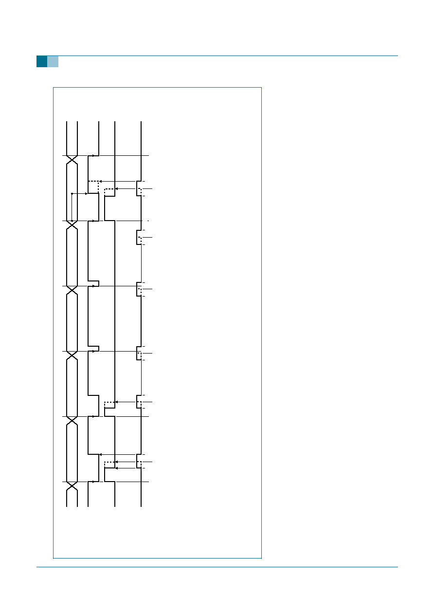
6.
Bloc
k dia
gram
Fig 1.
Block diagram
001aad315
˜2
IF
FILTER
N1
I/Q MIXER
1st FM
AGC
GAIN
STABILIZER
CRYSTAL
OSCILLATOR
SOFT
MUTE
SDS
19
I
2
C-BUS
INTERFACE
MPX
DECODER
TUNING SYSTEM
mono
pilot
prog. div out
I
ref
ref. div out
MUX
SW PORT
VCO
18
16
15
12
3.7
X1
10 k
33 nF
33 nF
47
pF
27
pF
L1
120 nH
100 pF
10 nF
12 pF
14
13
11
GNDD
INTX
INTCON2
12
n.c.
17
n.c.
21
n.c.
22
23
24
25
26
INTCON1
TMUTE
VAFR
VAFL
MPXOUT
MPXIN
GNDA
CD2/INTCON3
V
CCD
GNDD
GNDD
SDA
BUSENABLE
VREFDIG
SCL
100 k
LIMITER
LEVEL
ADC
IF CENTER
FREQUENCY ADJUST
DEMODULATOR
IF COUNT
TEA5764HN
33 nF
33 nF
10
nF
29
n.c.
n.c.
GNDD
27
28
30
32
31
n.c.
40
33
34
35
36
37
38
39
FREQIN
XTAL
CD3
FM
antenna
RFIN1
RFIN2
GNDRF
CAGC
V
CCA
1
2
3
4
5
7
6
8
SWPORT
9
10
LOOPSW
CPOUT
LO1
LO2
CD1
RDS/RBDS
DECODER
20
INTERFACE
REGISTER
57 kHz BP
FILTER
PAUSE
DETECTOR
33 nF
47 k
33 nF
33 nF
PILLP
L3
L3
D1
D2

TEA5764HN_2
© Koninklijke Philips Electronics N.V. 2005. All rights reserved.
Product data sheet
Rev. 02 -- 9 August 2005
5 of 64
Philips Semiconductors
TEA5764HN
FM radio + RDS
7.
Pinning information
7.1 Pinning
7.2 Pin description
Fig 2.
Pin configuration
001aab459
TEA5764HN
n.c.
VREFDIG
SCL
INTCON1
BUSENABLE
TMUTE
SWPORT
VAFR
PILLP
VAFL
CD1
MPXOUT
LO2
MPXIN
LO1
GNDD
CPOUT
n.c.
LOOPSW
GNDA
SDA
n.c.
GNDD
GNDD
V
CCD
CD2/INTCON3
n.c.
INTCON2
GNDD
INTX
n.c.
CAGC
GNDRF
RFIN2
RFIN1
CD3
V
CCA
XTAL
FREQIN
n.c.
10
21
9
22
8
23
7
24
6
25
5
26
4
27
3
28
2
29
1
30
11
12
13
14
15
16
17
18
19
20
40
39
38
37
36
35
34
33
32
31
terminal 1
index area
Transparent top view
Table 3:
Pin description
Symbol
Pin
Description
LOOPSW
1
synthesizer PLL loop filter switch output
CPOUT
2
charge pump output of synthesizer PLL
LO1
3
local oscillator coil connection 1
LO2
4
local oscillator coil connection 2
CD1
5
VCO supply decoupling capacitor
PILLP
6
pilot PLL loop filter
SWPORT
7
software programmable port output
BUSENABLE
8
I
2
C-bus enable input
VREFDIG
9
digital reference voltage for I
2
C-bus signals
SCL
10
I
2
C-bus clock line input
SDA
11
I
2
C-bus data line input and output
n.c.
12
not connected
GNDD
13
digital ground
GNDD
14
digital ground
V
CCD
15
digital supply voltage
CD2/INTCON3
16
internally connected

TEA5764HN_2
© Koninklijke Philips Electronics N.V. 2005. All rights reserved.
Product data sheet
Rev. 02 -- 9 August 2005
6 of 64
Philips Semiconductors
TEA5764HN
FM radio + RDS
8.
Functional description
8.1 Low noise RF amplifier
The LNA input impedance together with the LC RF input circuit defines an FM band filter.
The gain of the LNA is controlled by the RF AGC circuit.
8.2 FM I/Q mixer
FM quadrature mixer converts FM RF (76 MHz to 108 MHz) to IF.
8.3 VCO
The varactor tuned LC VCO provides the Local Oscillator (LO) signal for the FM
quadrature mixer. The VCO frequency range is 150 MHz to 217 MHz.
n.c.
17
not connected
INTCON2
18
internally connected; leave open
GNDD
19
digital ground
INTX
20
interrupt flag output
n.c.
21
not connected
INTCON1
22
internally connected; leave open
TMUTE
23
soft mute time-constant capacitor
VAFR
24
right audio output
VAFL
25
left audio output
MPXOUT
26
FM demodulator MPX output
MPXIN
27
MPX decoder and RDS decoder MPX input
GNDD
28
digital ground; this pin has an internal pull-down resistor of 10 k
to
ground
n.c.
29
not connected
GNDA
30
analog ground
n.c.
31
not connected
FREQIN
32
32.768 kHz reference frequency input
XTAL
33
crystal oscillator input
V
CCA
34
analog supply voltage
CD3
35
V
CCA
decoupling capacitor
RFIN1
36
RF input 1
RFIN2
37
RF input 2
GNDRF
38
RF ground
CAGC
39
RF AGC time-constant capacitor
n.c.
40
not connected
Table 3:
Pin description
...continued
Symbol
Pin
Description

TEA5764HN_2
© Koninklijke Philips Electronics N.V. 2005. All rights reserved.
Product data sheet
Rev. 02 -- 9 August 2005
7 of 64
Philips Semiconductors
TEA5764HN
FM radio + RDS
8.4 Crystal oscillator
The crystal oscillator can operate with a 32.768 kHz clock crystal. The oscillator can be
overridden via the FREFIN pin. When the FREFIN pin is used the oscillator is clocked
externally by a 32.768 kHz signal. Selection between a reference clock or a reference
crystal can be done via the I
2
C-bus. When a crystal is connected the FREFIN pin must be
left open-circuit, and when pin FREFIN is used a crystal may not be connected. It is not
possible to connect a crystal and apply a frequency via the FREFIN pin in the same
application.
The crystal oscillator generates the reference frequency for the following:
∑
Reference frequency divider for synthesizer PLL
∑
Timing for the IF counter
∑
Timing for the pause detector
∑
Free running frequency adjustment of the stereo decoder VCO
∑
Centre frequency for adjustment of the IF filters
∑
Clock frequency of the RDS/RBDS decoder
8.5 PLL tuning system
The PLL synthesizer tuning system is suitable to operate with a 32.768 kHz reference
frequency generated by the crystal oscillator or a reference clock of 32.768 kHz fed into
the TEA5764HN. To tune the radio to the required frequency requires the PLL word to be
calculated and then programmed to the register. The PLL word is 14 bits long; see
Table 20
and
Table 21
. Calculation of this 14-bit word can be done as follows.
Formula for high-side injection:
(1)
Formula for low-side injection:
(2)
where:
N
DEC
= decimal value of PLL word
f
RF
= wanted tuning frequency (Hz)
f
IF
= intermediate frequency of 225 kHz
f
ref
= the reference frequency of 32.768 kHz
Example for receiving a channel at 100.1 MHz:
(3)
N
DEC
4
f
RF
f
IF
+
(
)
◊
f
ref
--------------------------------------
=
N
DEC
4
f
RF
f
IF
≠
(
)
◊
f
ref
--------------------------------------
=
N
DEC
4
100.1
10
6
◊
225
10
3
◊
+
(
)
◊
32768
------------------------------------------------------------------------
12246.704
=
=

TEA5764HN_2
© Koninklijke Philips Electronics N.V. 2005. All rights reserved.
Product data sheet
Rev. 02 -- 9 August 2005
8 of 64
Philips Semiconductors
TEA5764HN
FM radio + RDS
The result found using
Equation 1
or
Equation 2
must always be rounded to the lowest
integer value. If rounded down to the lowest integer value of N
DEC
= 12246, the PLL word
becomes 2FD6h.
This value can be written to register FRQSETLSB or FRQSETMSB via the I
2
C-bus and
the IC will then either start an autonomous search at this frequency or go to a preset
channel at this frequency. When the application is built according to the block diagram
shown in
Figure 1
, and with the preferred components, the PLL will settle to the new
frequency within 5 ms. The most accurate tuning is accomplished when a search is
followed by a preset to the same frequency.
The PLL is triggered by writing to any one of the bytes FRQSETMSB, FRQSETLSB,
TNCTRL1, TNCTRL2, TESTBITS, TESTMODE.
Accurate validation of the PLL locking on the new frequency can take 2 ms to 10 ms.
When a lock is detected, bit LD is set.
8.6 Band limits
The TEA5764HN can be switched either to the Japanese FM-band or to the US/Europe
FM-band. Setting bit BLIM to logic 0 the band range is 87.5 MHz to 108 MHz; setting bit
BLIM to logic 1 selects the Japanese band range of 76 MHz to 90 MHz.
8.7 RF AGC
The RF AGC (or wideband AGC) prevents overloading and limits the amount of
intermodulation products created by strong adjacent channels. The RF AGC is on by
default and can be turned off via the I
2
C-bus.
The TEA5764HN also has an in-band AGC to prevent overloading by the wanted channel.
The in-band AGC is always turned on.
8.8 Local or long distance receive
If bit LDX = 1, the LNA gain is reduced by 6 dB to prevent distortion when a transmitter is
very near. If bit LDX = 0, the LNA gain is normal to receive long distance (DX) stations.
8.9 IF filter
A fully integrated IF filter is built-in.
8.10 FM demodulator
The FM quadrature demodulator has an integrated resonator to perform the phase shift of
the IF signal.
8.11 IF counter
The received signal is mixed to produce an IF of 225 kHz. The result of the mixing is
counted. A good IF count result indicates that the radio is tuned to a valid channel instead
of an image or a channel with much interference. The IF counter outputs a 7-bit count
result via the I
2
C-bus. The IF counter is continuously active and can be read at any time
via the I
2
C-bus. It also activates a flag when the IF count result is outside the IF count
valid result window; see
Section 9.1.4.4
.

TEA5764HN_2
© Koninklijke Philips Electronics N.V. 2005. All rights reserved.
Product data sheet
Rev. 02 -- 9 August 2005
9 of 64
Philips Semiconductors
TEA5764HN
FM radio + RDS
Before a tuning cycle is initiated the IF count period can be set to 2 ms or to 15.6 ms by
bit IFCTC. When the IF count period is set to 2 ms, initiating the tuning algorithm with a
preset (bit SM = 0) will always give an RDS update as shown in
Section 8.22.1
. In case
the IF count time is set to 15.6 ms, the tuning flowchart illustrated in
Figure 3
is used.
Once tuned, the IF count period is always 15.6 ms.
8.12 Voltage level generator and analog-to-digital converter
The voltage level indicates the field strength received by the antenna. The voltage level is
analog-to-digital converted to a 4-bit word and output via the I
2
C-bus. The ADC level is
continuously active and can be read at any time via the I
2
C-bus. It also activates a flag
when the voltage level falls below a predefined selectable threshold. Bit LHSW allows
either large or small hysteresis steps to be chosen; see
Table 24
and
Section 9.1.4.5
.
When the ADC level is set to 3, its minimum value, the search algorithm will only stop at
channels having a RF level higher than, or equal to, ADC level 3. After completing the
search algorithm and being tuned to a station, due to hysteresis the effective limit will be
set to 0. This means that the continuous ADC level check will never set the LEVFLAG.
8.13 Mute
8.13.1 Soft mute
The low-pass filtered voltage level drives the soft mute attenuator at low RF input levels:
the audio output is faded and hence also the noise (see
Figure note 1
in
Figure 15
and
Figure 17
).
The soft mute function can also be switched off via the I
2
C-bus, using bit SMUTE.
8.13.2 Hard mute
The audio outputs VAFL and VAFR can be hard-muted by bit MU in byte TNCTRL2, which
means that they are put into 3-state. This can also be done by setting bits Left Hard Mute
(LHM) or Right Hard Mute (RHM) in byte TESTBITS, which allows either one or both
channels to be muted and forces the TEA5764HN to mono mode. When the TEA5764HN
is in Standby mode the audio outputs are hard-muted.
8.13.3 Audio frequency mute
The audio signal is muted by setting bit AFM of the TNCTRL1 register to logic 1. In the
soft mute attenuator the audio signal is blocked and so pins VAFL and VAFR will be at
their DC biasing point with no signal.
The audio is automatically muted during an RDS update as shown in the flowchart of
Figure 3
. When the audio must be muted during Search mode, it is done by setting bit
AFM to logic 1 before the search action and resetting it to logic 0 afterwards.
Setting bit AFM to logic 0 stops the RDS data.
8.14 MPX decoder
The PLL stereo decoder is adjustment free. It can be switched to mono via the I
2
C-bus.

TEA5764HN_2
© Koninklijke Philips Electronics N.V. 2005. All rights reserved.
Product data sheet
Rev. 02 -- 9 August 2005
10 of 64
Philips Semiconductors
TEA5764HN
FM radio + RDS
8.15 Signal dependent mono/stereo blend (stereo noise cancellation)
If the RF input level decreases, the MPX decoder blends from stereo to mono to limit the
output noise. The continuous mono-to-stereo blend can also be programmed via the
I
2
C-bus to an RF level dependent switched mono-to-stereo transition. Stereo noise
cancellation can be switched off via the I
2
C-bus by bit SNC.
8.16 Software programmable port
One software programmable port (CMOS output) can be addressed via the I
2
C-bus:
Bit SWPM = 1, the software port functions as the output for the FRRFLAG.
Bit SWPM = 0, the software port outputs bit SWP of the registers.
In Test mode the software port outputs signals according to
Table 27
. Test mode is
selected, setting bit TM of byte TESTMODE to logic 1.
The software port cannot be disabled by the PUPD bits; see
Section 8.17
.
8.17 Standby mode
The radio can be put into Standby mode by the Power-Up / Power-Down (PUPD) bits. The
RDS part can be turned off separately or both the RDS and the FM part can be turned off.
The TEA5764HN is still accessible via the I
2
C-bus but takes only a low power from the
supply, in Standby mode, the audio outputs are hard-muted.
8.18 Power-on reset
After startup of V
CCA
and V
CCD
a power-on reset circuit will generate a reset pulse and the
registers will be set to their default values. The power-on reset is effectively generated by
V
CCD
.
After a power-on reset the TEA5764HN is in Standby mode and the PUPD bits are set to
logic 0. After a power-on reset the registers are reset to their default value, except for
byte12R to byte19R and flags DAVFLG, LSYNCFLG and PDFLAG. To reset these, the
RDS part must be turned on by setting PUPD. After setting PUPD to logic 1, it will take
0.9 ms to start-up the TEA5764HN and set these registers to their default value.
The power supplies can be switched on in any order.
When the supply voltage V
CCA
and V
CCD
are at 0 V, all I/Os, the audio outputs and the
reference clock input are high-ohmic.
8.19 RDS/RBDS
8.19.1 RDS/RBDS demodulator
A fully integrated RDS/RBDS demodulator which uses the reference frequency
(32.678 Hz) of the PLL synthesizer tuning system. The RDS demodulator recovers and
regenerates the continuously transmitted RDS or RBDS data stream of the multiplex
signal (MPXRDS) and provides the signals clock (RDCL), data (RDDA) for further
processing by the integrated RDS decoder.

TEA5764HN_2
© Koninklijke Philips Electronics N.V. 2005. All rights reserved.
Product data sheet
Rev. 02 -- 9 August 2005
11 of 64
Philips Semiconductors
TEA5764HN
FM radio + RDS
8.19.2 RDS data and clock direct
The RDS demodulator retrieves the RDS data and clock signals, this data can be put
directly onto pins VAFL and VAFR by setting bit RDSCDA to logic 1.
8.19.2.1
RDS/RBDS decoder
The RDS decoder provides block synchronization, error correction and flywheel function
for reliable extraction of RDS or RBDS block data. Different modes of operation can be
selected to fit different application requirements. Availability of new data is signalled by bit
DAVFLG and output pin INTX which generates an interrupt. Up to two blocks of data and
status information are available via the I
2
C-bus in a single transmission.
The behavior of the DAVFLG is described in
Section 10
.
8.20 Audio pause detector
The audio pause detector monitors the audio modulation for pauses and responds to low
levels. The modulation threshold can be adjusted in 4 steps of 4 dB by control bits PL[1:0].
The minimum time for detecting a pause can be adjusted by control bits PT[1:0] as shown
in
Table 38
. When a pause occurs, flag PDFLAG is set to logic 1 and a hardware interrupt
is generated; see
Section 9.1.4.6
.
8.21 Auto search and Preset mode
In Search mode the TEA5764HN can search channels automatically; see
Figure 3
.
TEA5764HN_2
© Koninklijke Philips Electronics N.V. 2005. All rights reserved.
Product data sheet
Rev. 02 -- 9 August 2005
12 of 64
Philips Semiconductors
TEA5764HN
FM radio + RDS
Before starting a search or a preset, the INTMSK register must be reset and only the
FRRMSK must be set. This allows the microprocessor to be interrupted only when the
search or preset algorithm is ready.
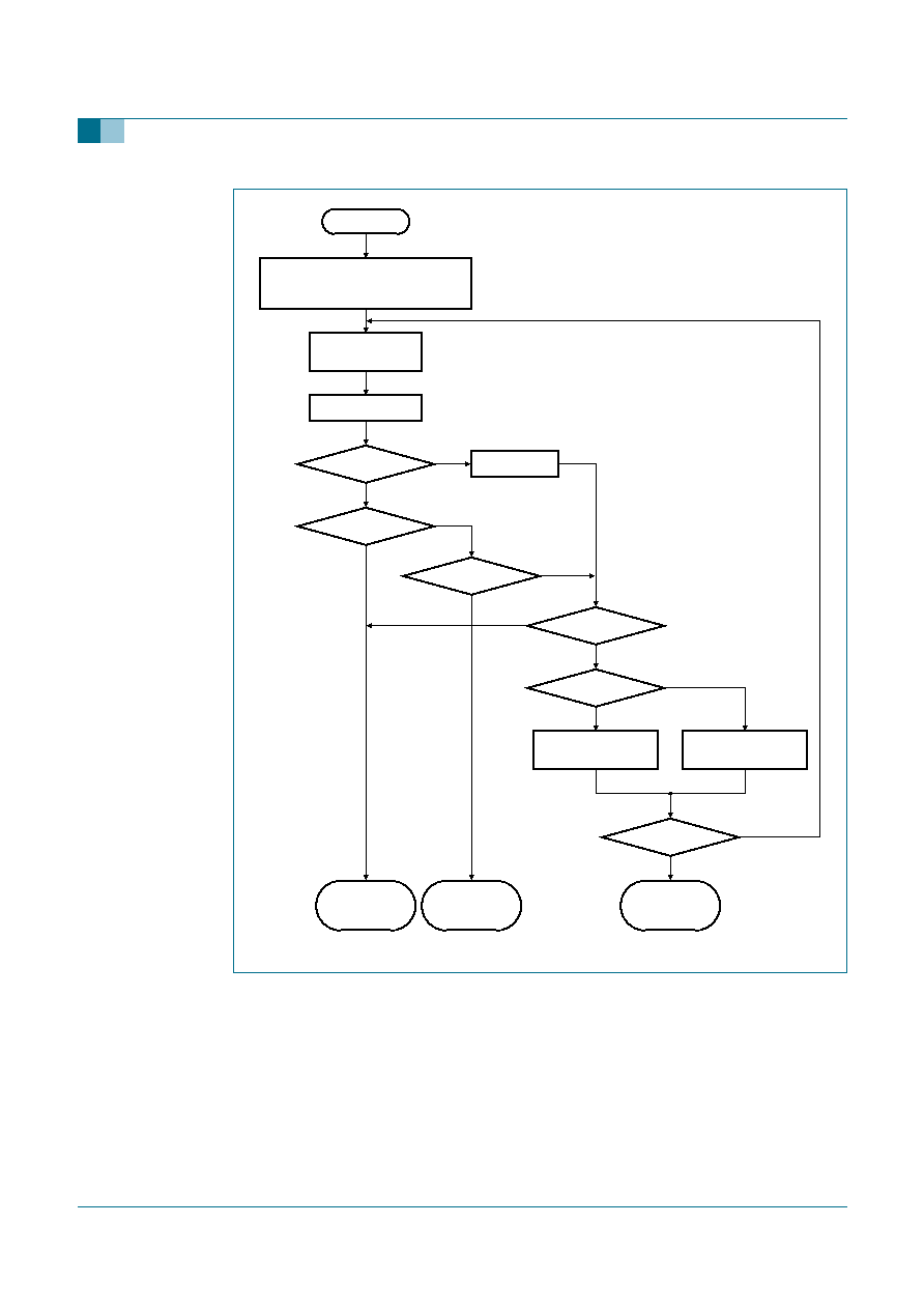
Fig 3.
Flowchart auto search or preset
001aab461
during a preset mute is always active
search mode is default not muted
unless AHLSI is set
BLFLAG = 0
FRRFLAG = 1
no mute
reset flags
set PLL frequency
increment current_pll
by 100 kHz
decrement current_pll
by 100 kHz
wait for PLL to settle
set LEVFLAG
true
false
level OK
start
true
false
IF OK
true
false
AHLSI
false
search up
true
true
false
band limit
true
false
search mode
BLFLAG = 0
FRRFLAG = 1
mute
BLFLAG = 1
FRRFLAG = 1
no mute

TEA5764HN_2
© Koninklijke Philips Electronics N.V. 2005. All rights reserved.
Product data sheet
Rev. 02 -- 9 August 2005
13 of 64
Philips Semiconductors
TEA5764HN
FM radio + RDS
8.21.1 Search mode
Search mode is initiated by setting bit SM in byte FRQSETMSB to logic 1. The search
direction is set by bit SUD; SUD = 0 (search down), bit SUD = 1 (search up). The tuner
starts searching at the frequency set in bytes FRQSETLSB and FRQSETMSB. The
Search Stop Level (SSL) bits define the field strength level at which a desired channel is
detected. The tuner will stop on a channel with a field strength equal to or higher than this
reference level and then checks the IF frequency; when both are valid, the search stops
(Note that this depends on bit AHLSI described in
Figure 3
). If the level check or the IF
count fails, the search continues. If no channels are found, the TEA5764HN stops
searching when it has reached the band limit, setting the BLFLAG HIGH. A search always
stops when the FRRFLAG is set and on the occurrence of a hardware interrupt, this
procedure is shown in
Figure 3
.
The search algorithm can stop at a frequency that is offset from the IF by up to a
maximum of 12 kHz. The maximum offset can be limited to 8 kHz by applying a preset.
For optimum tuning, it is recommended that a preset is applied after a search and when
the found frequency has an offset that is above 8 kHz.
After this interrupt the TEA5764HN will not update the tuner registers for a period of 15
ms. The state of the TEA5764HN can be checked by reading the bytes of INTFLAG,
FRQCHKMSB, FRQCHKLSB, TNCTRL1 and TNCTRL2.
Table 4
shows the possible
states of these registers after an auto search.
[1]
This table is valid until 30.6 ms after the tuning cycle has completed. It shows the outcome of the flag
register when a read is done after pin INTX goes LOW on condition that no mask bit other than FRRMSK is
set.
8.21.2 Preset mode
A preset occurs by setting bit SM to logic 0 and writing a frequency to byte FRQSETMSB.
The tuner jumps to the selected frequency and sets the FRRFLAG when it is ready.
After this interrupt the TEA5764HN will not update the tuner registers for a period of
15 ms. The state of the TEA5764HN can be checked by reading registers: INTFLAG,
FRQCHKLSB, FRQCHKMSB, TNCTRL1 and TNCTRL2.
Table 4
shows the possible
states after a preset.
Table 4:
Tuner truth table
[1]
IFFLAG BLFLAG
FRRFLAG Comment
0
0
0
if pin INTX has gone LOW and only IFMSK, FRRMSK and
BLMSK were set then this cannot occur
0
0
1
channel found during search / preset; FRRMSK set
0
1
0
not a valid state
0
1
1
a valid channel found and the band limit has been reached
during a search; BLMSK or FRRMSK set
1
0
0
not a valid state
1
0
1
a preset or search has occurred but the wanted channel has a
valid RSSI level but fails the IF count when AHLSI was set to
logic 1; HLSI must be toggled and a new PLL value must be
programmed; FRRMSK set
1
1
0
not a valid state
1
1
1
band limit is reached during search; no valid channel found;
BLMSK or FRRMSK set
TEA5764HN_2
© Koninklijke Philips Electronics N.V. 2005. All rights reserved.
Product data sheet
Rev. 02 -- 9 August 2005
14 of 64
Philips Semiconductors
TEA5764HN
FM radio + RDS
8.21.3 Auto high-side and low-side injection stop switch
When a channel is searched or a preset is done, reception can sometimes improve when
injection is done at the other side of the wanted channel.
The TEA5764HN has bit HLSI which toggles the injection of the local oscillator from
high-side (bit HLSI = 1) to low-side (bit HLSI = 0). When bit HLSI is toggled, a new PLL
setting must be sent to the TEA5764HN.
When bit AHLSI is set to logic 1, the search / preset algorithm will stop after a channel has
a valid RSSI level check but fails the IF count. The microprocessor can now respond by
toggling the HLSI switch and sending a new PLL value to the tuner.
8.21.4 Muting during search or preset
During a preset the tuner is always muted and this is implemented by the algorithm.
A search is not muted by default unless bit AFM = 1 or bit AHLSI = 1.
When bit AHLSI = 1 and the tuner stopped during a preset or a search because of a
wrong IF count, the tuner stays muted; this allows the microprocessor to switch from the
high to low setting quietly and wait for the new result.
The tuner is always muted if bit AFM = 1 and is independent of a search or a preset. A
search can be muted by setting bit AFM to logic 1 before a search is initiated and resetting
it to logic 0 when the tuner is ready (only set bit FRRMSK when initiating a search or
preset).
All these mute actions are done by blocking the audio signal inside the soft mute
attenuator, the audio output will keep its DC level and stay low-ohmic i.e. 50
(a hard
mute set by bit MU will cause a plop).
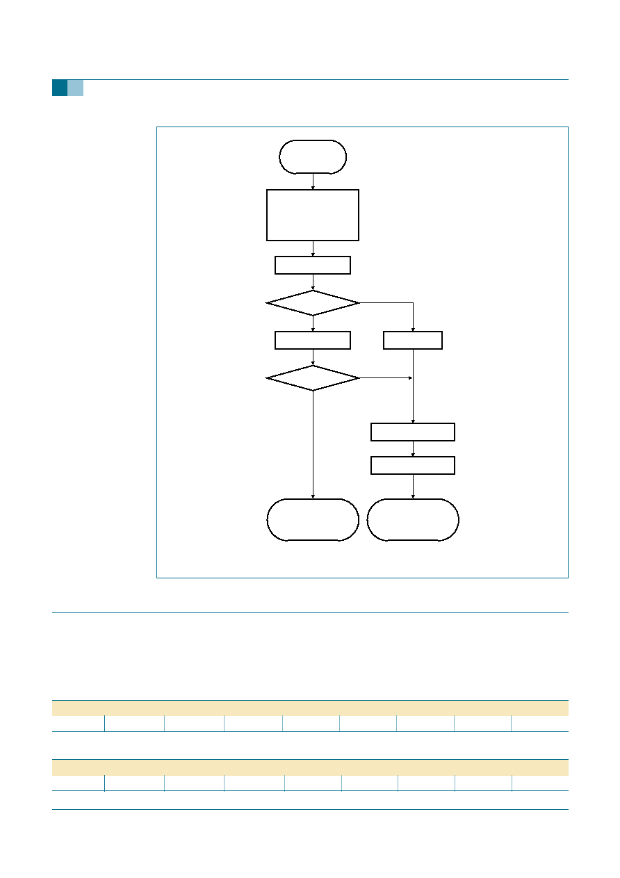
8.22 RDS update/alternative frequency jump
A channel which transmits RDS data can have alternative channels which have the same
information. These alternative channel frequencies are in the RDS data, so the
microprocessor can read the alternative frequencies and store them in a memory.
The tuner can perform an RDS update. This is very similar to a preset, but with a 2 ms IF
count time. The tuner will jump to the alternative frequency and check the level and the IF
count using a 2 ms count time. When the RSSI level check is above the specified level and
the IF count result is within the limits, then the tuner will stay at the alternative frequency
and stay muted, the microprocessor can now decide what to do. If the alternative
frequency is not valid it will jump back to the frequency it came from.
Fig 4.
Switch LO from high-side injection to low-side injection using bit HLSI
001aab460
image on high-side
wanted channel
switch LO from high-side to low-side
image on low-side

TEA5764HN_2
© Koninklijke Philips Electronics N.V. 2005. All rights reserved.
Product data sheet
Rev. 02 -- 9 August 2005
15 of 64
Philips Semiconductors
TEA5764HN
FM radio + RDS
The algorithm will finish with the FRRFLAG being set and an interrupt is generated. After
this interrupt the TEA5764HN will not measure the IF count for a period of 15 ms. 15 ms
after completing a RDS jump, a measurement of the IF count will start and hence the IF
count result and the IFFLAG will be updated 30.6 ms after completing the algorithm. The
level measurement will start immediately after the tuning algorithm, so the LEVFLAG will
be updated 500
µ
s after the algorithm. The state of the TEA5764HN can be checked by
reading registers INTFLAG, FRQCHKLSB, FRQCHKMSB, IFCHK and LEVCHK.
Table 5
shows the possible states after an auto search,
Figure 5
shows how the RDS is updated.
8.22.1 Muting during RDS update
An RDS update (AF jump) is always muted. There are two possibilities for leaving the
algorithm:
∑
The tuner jumps to an alternative frequency which is not valid (according to the
specified SSL limit and fixed IF counter limits) and jumps back, then it will
automatically unmute
∑
Or the tuner jumps to a valid alternative frequency and stays there. Now it does not
unmute. The microprocessor can unmute or it keeps the tuner muted and can check
for the presence of RDS data. The valid way to unmute is to apply a preset to the
current frequency (an IF count time of 15.6 ms is used at preset, which gives a more
accurate IF count result than the result obtained by the AF jump, where 2 ms is used)
[1]
This table is valid until 30.6 ms after an RDS update has completed. It shows the outcome of the flag
register when a read is done after pin INTX has gone LOW and on condition that only mask bit FRRMSK is
set.
Table 5:
RDS update truth table
[1]
IFFLAG BLFLAG
FRRFLAG Comment
0
0
0
if pin INTX is LOW and only IFMSK, FRRMSK and BLMSK were
set then this cannot occur
0
0
1
alternative frequency jump successful; radio is tuned to the
alternative frequency and stays muted
0
1
0
not a valid state
0
1
1
not a valid state
1
0
0
not a valid state
1
0
1
AF jump has occurred but the wanted channel fails the IF count;
the PLL will be set back to the old value
1
1
0
not a valid state
1
1
1
if pin INTX is LOW and only IFMSK, FRRMSK and BLMSK were
set then this cannot occur
TEA5764HN_2
© Koninklijke Philips Electronics N.V. 2005. All rights reserved.
Product data sheet
Rev. 02 -- 9 August 2005
16 of 64
Philips Semiconductors
TEA5764HN
FM radio + RDS
9.
Interrupt handling
9.1 Interrupt register
The first two bytes of the I
2
C-bus register contain the interrupt masks and the interrupt
flags. A flag is set when it is a logic 1.
Fig 5.
Flowchart RDS update
001aab462
activate mute
store 'old' PLL setting
clear LEVFLAG
clear IFFLAG
set PLL to AF frequency
FRRFLAG = 1
BLFLAG = 0
keep mute
(PLL is AF frequency)
FRRFLAG = 1
BLFLAG = 0
not mute
(PLL is old frequency)
wait for PLL to settle
set LEVFLAG
true
false
level OK
wait for IF counter
reset 'old' PLL setting
false
true
IF OK
wait for PLL to settle
start
set IF count time
to 2 ms
Table 6:
INTFLAG - byte0R
Bit
7
6
5
4
3
2
1
0
Symbol
DAVFLG
TESTBIT
LSYNCFLG
IFFLAG
LEVFLAG
PDFLAG
FRRFLAG
BLFLAG
Table 7:
INTMSK - byte0W / byte1R
Bit
7
6
5
4
3
2
1
0
Symbol
DAVMSK
-
LSYNCMSK
IFMSK
LEVMSK
PDMSK
FRRMSK
BLMSK

TEA5764HN_2
© Koninklijke Philips Electronics N.V. 2005. All rights reserved.
Product data sheet
Rev. 02 -- 9 August 2005
17 of 64
Philips Semiconductors
TEA5764HN
FM radio + RDS
The interrupt flag register contains the flags set according to the behavior outlined in
Section 9.1.4
. When these flags are set they can also cause the INTX to go active
(hardware interrupt line) depending on the status of the corresponding mask bit in
Table 7
.
A logic 1 in the mask register enables the hardware interrupt for that flag.
Hence, it is conceivable that, with all the mask bits cleared, the software could operate in
a continuous polling mode that reads the interrupt flag register for any bits that maybe set.
Interrupt mask bits are always cleared after reading the first two bytes of the interrupt
register. This is to control multiple hardware interrupts (see
Figure 6
). Bit LSYNCMSK has
a different function and is not cleared after reading the interrupt register bytes; see also
Section 9.1.4.3
.
9.1.1 Interrupt clearing
The interrupt flag and mask bits are always cleared after:
∑
They have been read via the I
2
C-bus
∑
A power-on reset
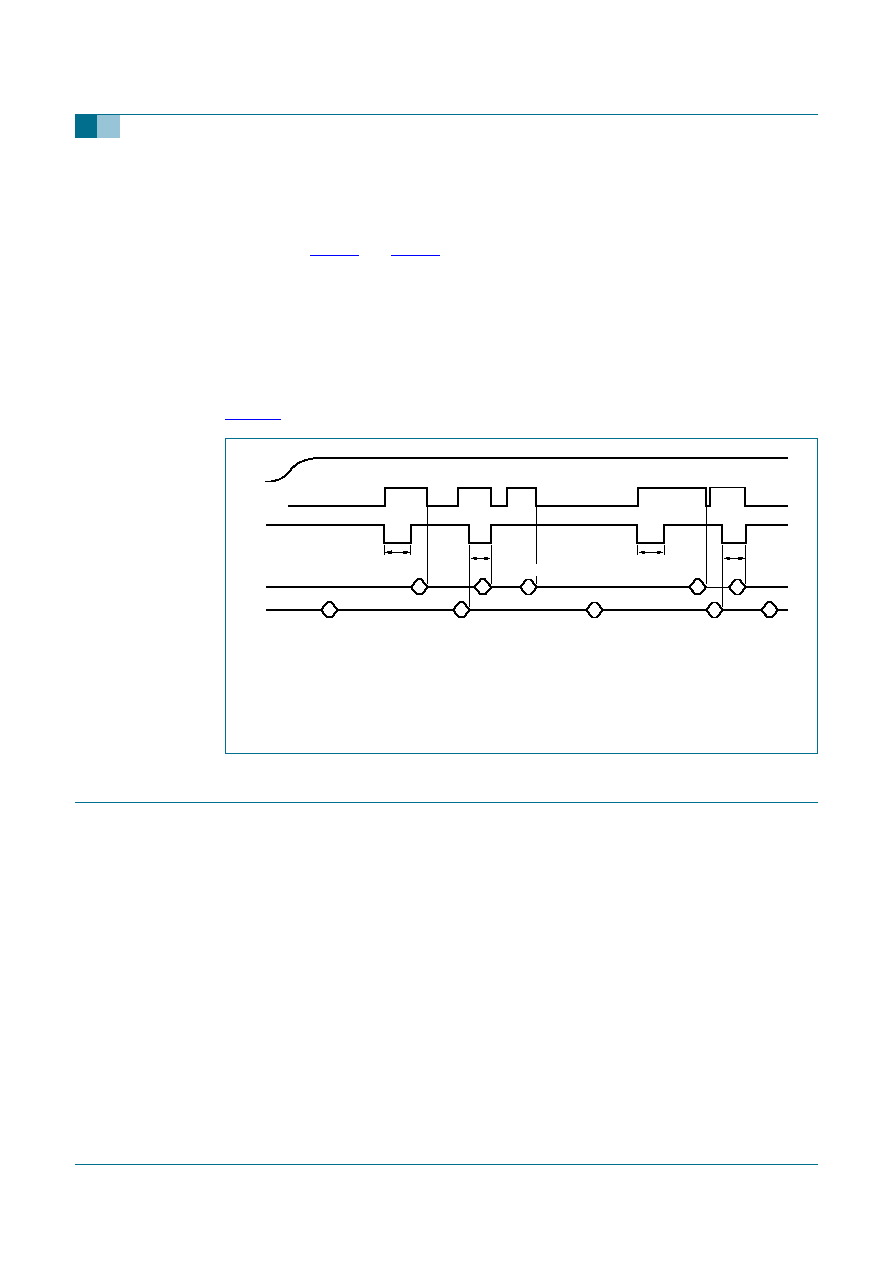
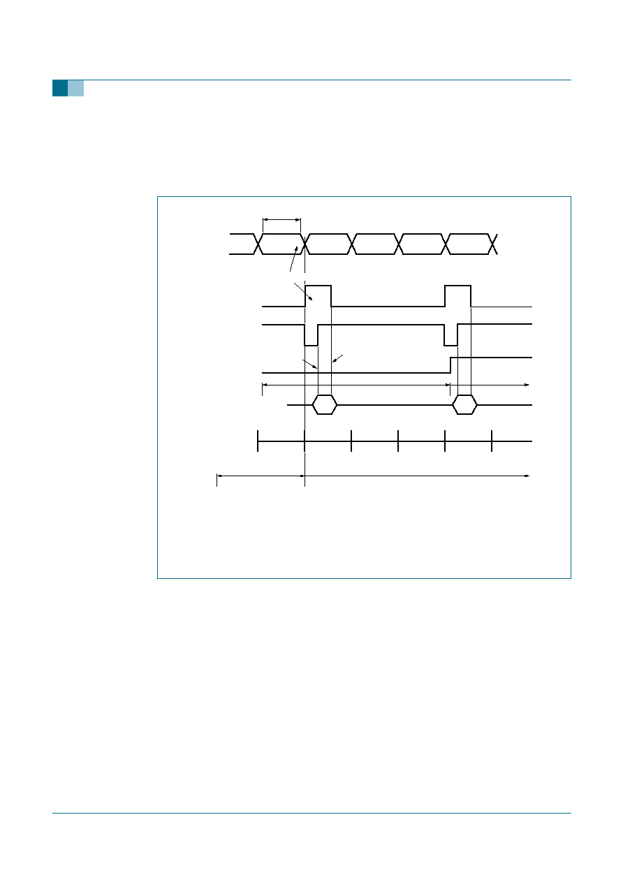
9.1.2 Timing
The timing sequence for the general operation interrupts is shown in
Figure 6
and shows
a read access of the interrupt bytes INTFLAG and INTMSK and a subsequent (though not
necessarily immediate) write to the mask register. It also indicates the two key timing
points A and B.
If an interrupt event occurs while the register is being accessed (after point A) it must be
held until after the mask register is cleared at the end of the read operation (point B).
Point A is after the R/W bit has been decoded and point B is where the acknowledge has
been received from the master after the first two bytes have been sent.
The LOW time for the INTX line (t
LOW
) has a maximum value specified in
Section 15
.
However it can be shorter if the read of the INTMSK and INTFLAG bytes occurs within
t
LOW
.
9.1.3 Reset
A reset can be performed at any time by a simple read of the interrupt bytes, byte0R and
byte0W, which automatically clears the interrupt flags and masks.

xxxxxxxxxxxxxxxxxxxxx xxxxxxxxxxxxxxxxxxxxxxxxxx xxxxxxx x x x xxxxxxxxxxxxxxxxxxxxxxxxxxxxxx xxxxxxxxxxxxxxxxxxx xx xx
xxxxx xxxxxxxxxxxxxxxxxxxxxxxxxxx xxxxxxxxxxxxxxxxxxx xxxxxx xxxxxxxxxxxxxxxxxxxxxxxxxxxxxxxxxxx xxxxxxxxxxxx x x
xxxxxxxxxxxxxxxxxxxxx xxxxxxxxxxxxxxxxxxxxxxxxxxxxxx xxxxx xxxxxxxxxxxxxxxxxxxxxxxxxxxxxxxxxxxxxxxxxxxxxxxxxx xxxxxxxx
xxxxxxxxxxxxxxxxxxxxxxxxx xxxxxxxxxxxxxxxxxxxx xxx
TEA5764HN_2
© K
oninklijk
e Philips Electronics N.V
. 2005. All r
ights reser
v
ed.
Pr
oduct data sheet
Re
v
.
02 -- 9 A
ugust 2005
18 of 64
Philips Semiconductor
s
TEA5764HN
FM radio + RDS
(1) Interrupt events that occur outside of the region A-B set their respective flag bits in the normal way immediately and can thus trigger a hardware interrupt if the mask
bits are set.
(2) The blocking of interrupts is marked by the region A-B
1
/ B
2
depending on the actual read cycle.
B
1
is when only the INTFLAG is read and a stop condition is received (only INTFLAG is read so only this will be cleared).
B
2
is when both registers are read and hence cleared and this is terminated by either an acknowledge or stop bit.
(3) Interrupt events that occur between A and B set their respective flags after the mask bits are cleared. Which means that in this diagram an interrupt event occurred in
period A-B, so after A-B the flag goes to logic 1.
(4) All interrupt mask bits are cleared after the interrupt flag and mask bytes are read.
(5) Software writes to the mask byte and enables the required mask bits. Any flags currently set will then trigger a hardware interrupt.
(6) INTX is set HIGH (inactive) after the interrupt mask bytes are read.
Fig 6.
I
2
C-bus interrupt sequence, read and write operation
001aab464
device
address
INTFLAG
INTMSK
read access
data
INTMSK
FRQSETMSB
FRQSETLSB
write access
S
R
A
interrupt event
interrupt flag bit
0R data
A
A
(1)
(2)
(3)
interrupt mask bit
(4)
(5)
(6)
(5)
B
1
B
2
1R data
A
data
A
device
address
S
P
W
A
0W data
A
1W data
A
2W data
A
INTX

TEA5764HN_2
© Koninklijke Philips Electronics N.V. 2005. All rights reserved.
Product data sheet
Rev. 02 -- 9 August 2005
19 of 64
Philips Semiconductors
TEA5764HN
FM radio + RDS
9.1.4 Interrupt flags and behavior
9.1.4.1
Multiple interrupt events
If the interrupt mask register bit is set then the setting of an interrupt flag for that bit
causes a hardware interrupt (pin INTX goes LOW). If the event occurs again, before the
flag is cleared, then this does not trigger any further hardware interrupts until that specific
flag is cleared. However, two different events can occur in sequence and generate a
sequence of hardware interrupts. A second interrupt can be generated only after the
INTMSK byte is read, followed by a write as the first interrupt blocks the input of the INTX
one-shot generator.
If subsequent interrupts occur within the INTX LOW period then these do not cause the
INTX period to extend beyond its specified maximum period (see
Section 9.2
).
9.1.4.2
Data available flag
The DAVFLG is set when a new block of data is received according to
Figure 9
to
Figure 12
, where the different DAV modes are described. Once synchronized, this
continues for all subsequent received blocks (dependent on DAV mode) and in the
following situations:
∑
During sync search, in any DAV mode: two valid blocks in the correct sequence
received with BBC < BBL (synchronized).
∑
During synchronization search in DAVB mode if a valid A(C')-block has been
detected. This mode can be used for fast search tuning (detection and comparison of
the PI code contained in the A or C' block.
∑
If the pre-processor is synchronized and in mode DAVA and DAVB a new block has
been processed. This mode is the standard data processing mode if the decoder is
synchronized.
∑
If the pre-processor is synchronized and in DAVC mode, two new blocks have been
processed.
∑
If the decoder is synchronized and in any DAV mode, with LSYNCMSK = 0, loss of
synchronization is detected (flywheel loss of synchronization, resulting in a restart of
synchronization search).
The DAVFLG is reset by a read of RDSLBLSB (byte15R) or RDSPBLSB (byte17R). An
interrupt is asserted each time a new block of data is decoded and when bit DAVMSK is
set; see
Section 10
.
9.1.4.3
RDS synchronization flag
Bit SYNC,
Table 29
, shows the status of the RDS decoder. If it is a logic 1 then the
decoder is synchronized, if it is a logic 0 it is not.
The action of the TEA5764HN depends on the status of bit LSYNCMSK in
Table 7
. If this
is set then the loss of synchronization causes bit LSYNCFL to go to logic 1 when
synchronization is lost, and a hardware interrupt is asserted. The RDS part of the
TEA5764HN is set to idle and waits for the microprocessor to initiate a new
synchronization search by setting bit NWSY as described in
Table 36
.

TEA5764HN_2
© Koninklijke Philips Electronics N.V. 2005. All rights reserved.
Product data sheet
Rev. 02 -- 9 August 2005
20 of 64
Philips Semiconductors
TEA5764HN
FM radio + RDS
If bit LSYNCMSK is 0 and synchronization is lost, the ASIC automatically starts a new
synchronization search. It will not generate a hardware interrupt. The microprocessor can
wait until the RDS decoder is synchronized again, this will be indicated by the DAVFLG
and the SYNC status bit (this requires bit DAVMSK being set).
Bit LSYNCFL is reset by a read of the INTMSK byte1R.
Bit LSYNCMSK is not reset by a read of byte INTMSK, it must be set or reset by the
microprocessor. Resetting it automatically would change the status of the ASIC and cause
an automatic synchronization search as described above.
How the synchronization is defined is explained in brief in
Section 10
.
9.1.4.4
IF frequency flag
During an automatic frequency search, preset or AF update, the FM part of the
TEA5764HN performs a check of the received IF frequency as a measure of the level of
interference in the channel received. If an incorrect IF frequency is received, it indicates
the presence of either strong interferers or tuning to an image which sets bit IFFLAG in the
INTFLAG register. Also a preset to a channel with no signal will result in a wrong IF count
value and hence the setting of bit IFFLAG.
When a search, preset or AF update is finished, bit FRRFLAG will be set to indicate this
and will generate an interrupt. The microprocessor can now read the outcome of the
registers which will contain the IF count value and the IFFLAG status of the channel it is
tuned to. In the case of an AF update, the IF count value of the alternative frequency will
be in the registers and also when it jumps back, because it will then not start a new IF
count.
15 ms after the tuning algorithm has completed the IF counter will start a new count. So
30.6 ms after a failed AF update the IF count result will be equal again to that of the
channel from where the jump was initiated.
15 ms after the FRRFLAG has been set the IF counter will start to run continuously on the
tuned frequency and if the conditions for correct frequency are not met then this sets bit
IFFLAG in the interrupt register. When bit IFMSK is set this will also cause an interrupt.
Bit IFFLAG is cleared by a read of byte1R, or by starting the tuning algorithm.
9.1.4.5
RSSI threshold flag
The voltage level reflects the field strength received by the antenna. The voltage level is
analog to digital converted to a 4-bit value and output via the I
2
C-bus, this 4-bit level value
can be compared to a threshold level set by the SSL bits in
Table 19
or the LH bits in
Table 26
.
The ADC level (which converts the analog value to digital) can be triggered to convert in
either of two ways:
1. During a tuning step, a search, a preset or an AF update, it is triggered by these
algorithms and compares the level with the threshold set by bits SSL[1:0]. Bit
LEVFLAG is set if the RSSI level drops below the threshold level set by bits SSL[1:0];
see
Table 19
. The hardware interrupt is only generated if the corresponding mask bit
is set.

TEA5764HN_2
© Koninklijke Philips Electronics N.V. 2005. All rights reserved.
Product data sheet
Rev. 02 -- 9 August 2005
21 of 64
Philips Semiconductors
TEA5764HN
FM radio + RDS
2. After a search, a preset or an AF update, the threshold for comparison is switched to
the hysteresis level. The hysteresis level is set by the combination of bits SSL[1:0] and
bit LHSW; see
Table 24
. The result is a hysteresis as shown in
Table 26
. Then the
ADC level starts to run automatically and compares the level every 500
µ
s with the
hysteresis level. Bit LEVFLAG is set if the RSSI level drops below the threshold level
set by bits SSL[1:0] in combination with bit LHSW (see
Table 26
); the hardware
interrupt is only generated if the corresponding mask bit is set. Bit LHSW allows either
a small or a large hysteresis to be selected which results in the levels of the left RSSI
hysteresis threshold column for bit LHSW = 0 and the right RSSI hysteresis threshold
column; see
Table 26
. When a search or preset is done with the ADC level set to 3
then when the algorithm has finished, the threshold level is set to 0. Hence the
LEVFLAG will never be set.
Bit LEVFLAG is cleared by a read of the INTMSK byte1R, or by starting the tuning
algorithm.
9.1.4.6
Pause detection flag
The pause detector monitors the amplitude of the audio signal and starts counting if it
drops below the reference level. When the counter reaches the specified count time, a
pause is detected and the PDFLAG is set and will generate an interrupt if bit PDMSK is
set to logic 1. The PDFLAG operates independently of bit PDMSK and is only active when
the RDS decoder is switched on when bit PUPD is set to logic 1 and when the RDS
decoder is not idle if synchronization is lost.
See
Figure 7
. When the peak audio level of the (L+R) drops below the threshold level at t
1
it counts the duration of the pause. If the pause lasts longer than the value set by the PT
bits, bit PDFLAG is set which in turn generates a hardware interrupt (bit PDMSK set to
logic 1). The threshold level at t
1
is set by the PL bits shown in
Table 38
.
Bit PDFLAG is cleared by a read of byte1R on condition that the read action occurs more
than 500
µ
s after receiving the pause interrupt on the INTX line.
The circuit should ignore short transients where the audio level momentarily rises above
the threshold (at t
2
).
A pause is detected by comparing the amplitude of the audio signal with the reference
level selected by the PL bits. The resultant signal PSCO produced by this comparison is
sampled at a frequency of 2341 Hz resulting in signal PSCOn. A pause is detected under
the conditions given by
Equation 4
and
Equation 5
.
(4)
(5)
where N is the number of samples taken over time and PT is the pause time selected by
bus bits PT. When a pause is detected, the integrator will be reset. The integrator value
cannot be less than zero; therefore if in
Equation 4
, the value of the second SUM
becomes larger than the first SUM, the output of the integrator remains at zero.
Suppose that PT = 20 ms, t
pause
= 16 ms and t
audio
= 1.5 ms. The pause detector will
count according to
Equation 5
as shown in
Equation 6
:
(6)
SUM 0toN
1
≠
(
)
PSCOn
0
=
[
]
8
SUM 0toN
1
≠
(
)
◊
PSCOn
1
=
[
]
≠
{
}
PT
2341
◊
>
t
pause
8
t
audio
PT
>
◊
≠
2
t
pause
8
t
◊
≠
audio
◊
20 ms
2
16 ms
8
1.5 ms
◊
≠
◊
20 ms
=
=

TEA5764HN_2
© Koninklijke Philips Electronics N.V. 2005. All rights reserved.
Product data sheet
Rev. 02 -- 9 August 2005
22 of 64
Philips Semiconductors
TEA5764HN
FM radio + RDS
In
Equation 6
, the pause detector has measured 1
◊
16 ms `pause', 8
◊
1.5 ms `no pause'
and 1
◊
16 ms pause. Therefore on average the pause detector has measured 16 ms
-
12
ms + 16 ms = 20 ms pause time and hence a pause will be detected.
The PSCOn signal goes directly to the software port. The PDFLAG is set by the integrator
and goes to the bus. The interrupt line is triggered by the PDFLAG.
9.1.4.7
Frequency ready flag
The frequency ready flag bit is set to logic 1 when the automatic tuning has finished a
search, a preset or an RDS AF update. This bit is described in
Table 4
and
Table 5
. The
FRRFLAG is cleared by a read of byte1R.
t
np(min)
> 5 ms.
(1) The reference level is defined in kHz, but is internally transformed to mV e.g. 22.5 kHz = 75 mV; 1 kHz = 3.3 mV.
(2) The actual PSCO signal behaves as shown in the top diagram, in the bottom diagram it is assumed that all samples are
taken at peaks of the audio signal resulting in PSCOn.
Fig 7.
Operation and timing of pause detection according to levels set in
Table 38
001aac795
audio signal
PSCO
audio
0
(2)
no audio present
audio present
PT x 2341
+ reference level "PL" [mV] (1)
pause
no pause
-
reference level "PL"
0
PSCOn
t
pause
t
audio
t
pause
PDFLAG
integrator
output
t
1
t
2
TEA5764HN_2
© Koninklijke Philips Electronics N.V. 2005. All rights reserved.
Product data sheet
Rev. 02 -- 9 August 2005
23 of 64
Philips Semiconductors
TEA5764HN
FM radio + RDS
9.1.4.8
Band limit flag
The band limit bit BLFLAG is set to logic 1 when the automatic tuning has detected the
end of the tuning band or when the PLL cannot lock on a certain frequency. This bit is
described in
Table 4
and
Table 5
. This bit is cleared by reading byte1R.
9.2 Interrupt output
The interrupt line driver is a MOS transistor with a nominal sink current of 680
µ
A, it is
pulled HIGH by an 18 k
resistor connected to pin VREFDIG. The interrupt line can be
connected to one other similar device with an interrupt output and an 18 k
pull-up
resistor providing a wired OR function. This allows any of the drivers to pull the line LOW
by sinking the current. When a flag is set and not masked it generates an interrupt; see
Figure 8
.
10. RDS data processing
The RDS demodulator and decoder perform the following operations:
∑
Demodulation of the RDS/RDBS data stream from the MPX signal
∑
Symbol decoding
∑
Block and group synchronization
∑
Error detection and correction
∑
Store last and previous data block received with associated ID and error status
∑
Set the DAVFLG when new data is received
∑
Set the SYNC status bit according to the current synchronization state
∑
Set the LSYNCFL flag when synchronization is lost
The RDS decoder can be set to different modes, each meant to look for specific
information.
Read INTMSK clears flag, INTMSK and INTX.
Write INTMSK enables INTX.
When flag is set, the next interrupts are blocked until read / write INTMSK.
(1) Flag is set immediately after the reset, because event is still there.
Fig 8.
Interrupt line behavior
001aab470
V
CCA
flag
INTX
read INTMSK
10 ms
<
10 ms
read clears INTX
(1)
write INTMSK
10 ms
<
10 ms

TEA5764HN_2
© Koninklijke Philips Electronics N.V. 2005. All rights reserved.
Product data sheet
Rev. 02 -- 9 August 2005
24 of 64
Philips Semiconductors
TEA5764HN
FM radio + RDS
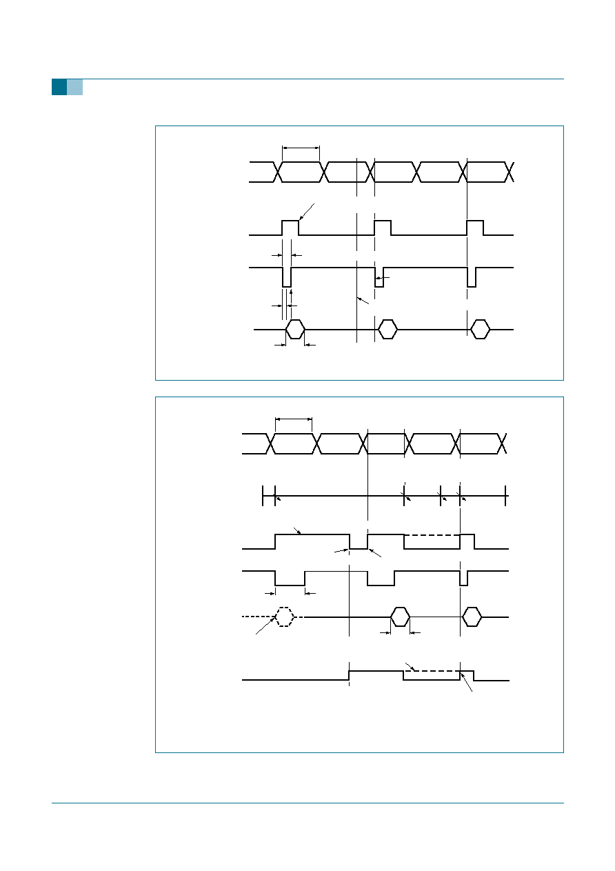
10.1 DAV-A processing mode
The DAV-A processing mode is the standard processing mode used. In this mode, when a
data block has been decoded, it is transferred to the I
2
C-bus registers. It generates
interrupts on the INTX line after every new block of RDS data that has been processed
and also sets the DAVFLG; see
Figure 9
. The DAVFLG is reset by a read of the I
2
C-bus
registers.
If a data block is decoded and a new one arrives, pin INTX goes LOW again, the DAVFLG
will be set and the last block will be shifted to the previous block and the last decoded
block will be put in the last block. This means that all RDS data is still available in the BL
and BP registers.
When the I
2
C-bus registers are not read the DAVFLG will not be reset. If a data block is
decoded and a new one arrives, pin INTX goes LOW and the last block will be shifted to
the previous block and the last decoded block will be put in the last block. This means that
all RDS data is still available in the BL and BP registers but must be read. This is indicated
by the setting of bit DOVF.
If the I
2
C-bus registers are still not read, data will be lost, except when this read is done
within 20 ms after the INTX line has gone LOW and 2 ms before the arrival of a new block.
If this read is done at least 2 ms before the arrival of a new block, then BL and BP are read
and the data in the decoder buffer is then instantaneously shifted to the BL register. All
data is now read and bit DOVF will be reset.

TEA5764HN_2
© Koninklijke Philips Electronics N.V. 2005. All rights reserved.
Product data sheet
Rev. 02 -- 9 August 2005
25 of 64
Philips Semiconductors
TEA5764HN
FM radio + RDS
Figure 9
assumes that block synchronization has been achieved and that no other
interrupt flags are being set.
10.2 DAV-B processing mode / fast PI search mode
This mode is used, for example, when the receiver has been re-tuned to a new station,
and a fast search of the PI code, always contained in the A or C' block, is required. The
diagram shown in
Figure 10
, assumes that the RDS decoder is unsynchronized initially
and is performing a synchronization search.
During synchronization search the decoder does not set the DAVFLG until a valid A or C'
block is detected. If a valid B block is detected immediately, then the decoder is now
synchronized and bit SYNC is set to logic 1. In fact, if any 2 good blocks in a valid order
are detected, the RDS decoder will synchronize and give an interrupt.
Bit DOVF set when 2 new blocks received in BL and BP registers
(1) If there is no read cycle, B
1
is placed in the BP register and the new block C
1
is now in the BL
register. Bit DOVF is set to indicate two blocks available.
(2) Data is not transferred to BL register at the end of the read period/clear DOVF, D
1
is missed.
(3) In order not to lose D
1
a read must be performed before D
1
enters decoder buffer, thus read
finishes within 21 ms after DOVF set to logic 1.
(4) DOVF is cleared when the BL register is read. To be of use, DOVF has to be read before BL
and BP registers.
(5) To prevent DOVF being set again, an extra read of BL must be performed before A2 has been
decoded.
Fig 9.
DAV-A timing diagram, DAV-A/B: normal
001aab471
A
1
21.9 ms
DAVFLG
DAVFLG set
on falling edge
DAVN = 0, cleared
on read BL register
INTX
B
1
read BL
end read intmsk
read intflg
+
RDS on INTX
t
INT_RD
t
READ
BL register
A
1
BP register
t
INT_RD
<
10 ms
read BL
read BL
C
1
D
1
A
2
B
2
C
2
B
1
(1)
(3)
(2)
(4)
(2)
(1)
(5)
C
1
D
1
B
2
x
A
1
B
1
C
1
A
2
being decoded
B
1
in the decoder buffer
data overflow bit
C
1
D
1
A
2
A
1
B
1
C
1
D
1
C
1
B
1
A
2
D
1
A
2
D
1
A
2
A
2
B
2
A
2
B
2
A
1
decoder
registers:
9.98 ms
9.98 ms
>
2 ms
TEA5764HN_2
© Koninklijke Philips Electronics N.V. 2005. All rights reserved.
Product data sheet
Rev. 02 -- 9 August 2005
26 of 64
Philips Semiconductors
TEA5764HN
FM radio + RDS
If for some reason a valid B block was not received then the next valid A or C' block is
decoded and the DAVFLG set. The BP and BL registers record the A block history.
When the decoder is synchronized, each decoded block will set the DAVFLG (assuming it
was reset by a read action) and generate an interrupt.
10.3 DAV-C reduced processing mode
The DAV-C processing mode is very similar to DAV-A mode with the main exception that a
data flag is set only after two new blocks are received. Hence the update rate is reduced
by half.
When the number of blocks detected in the order: `bad' `bad' `good' is 2, synchronization is
achieved if another good block followed by either 0, 1 or 2 bad blocks and another good block
are then received. If the order is 3 bad blocks, no synchronization is achieved and the counters
are reset.
Fig 10. DAV-A timing diagram, DAV B: with bad blocks detected during sync search
001aab472
B
1
21.9 ms
only valid blocks with no errors
are counted as good blocks
error correction applied
according to SYM bits
bad
good
good
good
bad
read BL register
read intmsk
not synchronized
synchronized
DAVFLG
INTX
sync status bit
good A or C' block detected
bad
C'
1
Bus access - read
D
1
A
2
B
2
C
2
BL register
x
BP register
C'
1
C'
1
C'
1
B
2
C
2
x
x
x
x
C'
1
B
2
TEA5764HN_2
© Koninklijke Philips Electronics N.V. 2005. All rights reserved.
Product data sheet
Rev. 02 -- 9 August 2005
27 of 64
Philips Semiconductors
TEA5764HN
FM radio + RDS
Fig 11. Normal DAV-C timing diagram
Fig 12. DAV-C timing diagram, late read of BL, BP register
001aab473
A
1
21.9 ms
B
1
DAVFLG cleared at end read BP register
and forced to zero till end read of RDS 4R
BL register copied to
BP register and C
1
to
BL register
B
1
copied to BL register shortly
before C
1
decoded
INTX cleared at end read INTMSK
t
INTX
t
INT_RD
t
read
DAVFLG
being
decoded
read access
(case 1)
INTX
C
1
D
1
A
2
B
2
001aab474
A
1
21.9 ms
B
1
DAVFLG reset when
1
st
new block
would have been copied
DAVFLG set when 2
nd
new block
in decoder buffer
instant copy of A
2
from decoder
buffer to BL, and
BL to BP
instant copy C
1
from decoder buffer
to BL, and BL to BP just before D
1
decoded due to read action
(a)
DAVFLG not cleared as no read performed
t
read
t
INTX
= 10 ms
INTX
read access
(case 2)
data
overflow bit
no read on INTX
so B
1
will be lost
2 new blocks have arrived in BL/BP (C
1
, D
1
) and a new block (A
2
)
has entered the decoder buffer. Hence, DOVF is set again.
To prevent this, an extra read must be performed after reading (a)
dashed line shows what would happen if no read
occurred at (a). DOVF bit set until the next read of BP
register, however D1, A2 would be lost
C
1
D
1
A
2
B
2
BL register
A
1
BP register
D
1
C
1
A
2
D
0
D
0
C
0
C
1
A
1
D
1
DAVFLG
(case 2)

TEA5764HN_2
© Koninklijke Philips Electronics N.V. 2005. All rights reserved.
Product data sheet
Rev. 02 -- 9 August 2005
28 of 64
Philips Semiconductors
TEA5764HN
FM radio + RDS
10.4 Synchronization
10.4.1 Conditions for synchronization
When the RDS decoder is turned on it must be synchronized to extract valid data from the
MPX signal. To do so the decoder automatically initiates a search for synchronization. The
conditions to meet synchronization and the status of this synchronization can be set and
checked by the following bits:
∑
BBL (Bad Blocks Lose): these bits can be set via the I
2
C-bus and have a value
between 0 to 63
∑
GBL (Good Blocks Lose): these bits can be set via the I
2
C-bus and have a value
between 0 to 63
∑
BBG (Bad Blocks Gain): these bits can be set via the I
2
C-bus and have a value
between 0 to 32
∑
GBC (Good Block Count): these bits can be read via the I
2
C-bus and have a value
between 0 to 63
∑
BBC (Bad Block Count): these bits can be read via the I
2
C-bus and have a value
between 0 to 63
When the decoder is not synchronized it will initiate a synchronization search. This
involves calculation of the syndrome for each block of 26 received bits on a bit-by-bit
basis. When a correct syndrome (and hence block ID) is received the decoder clocks the
next 26 bits into the internal registers and performs a second syndrome check.
Synchronization is found when a certain number of blocks have been decoded and two
good blocks have been found, this number of blocks is defined by the BBG bits. If the first
block needed for synchronization has been found and the expected second block (after 26
bits) is an invalid block, then the decoder module internal bad_blocks_counter is
incremented and the next expected block is calculated; exception: if RBDS mode is
selected and the first block is E, then the next expected block is always block A, until
synchronization is found or the maximum bad_blocks_counter value is reached. If the
decoder module internal bad_blocks_counter reaches the value of BBG[4:0], then a new
synchronization search (bit-by-bit) is started immediately to find a new first block.
The synchronization is monitored by two flywheel counters, GBC and BBC. These are
6-bit counters that can be preset by bits GBL and BBL to values between 0 and 63. Each
time a block is decoded and recognized as a bad block the Bad Block Counter value,
BBC, is incremented by 1. When the BBC value is equal to the BBL value, synchronization
is lost. Bit SYNC will become 0 and bit LSYNCFL is set to indicate the loss of
synchronization. The TEA5764HN will now automatically initiate a new synchronization
search.
Each time a good block is decoded, the GBC value is incremented. When the GBC value
is equal to the GBL value, both counters, BBC and GBC, are set to 0 and a new count
starts. The GBC counter is only incremented when the decoder is synchronized.

TEA5764HN_2
© Koninklijke Philips Electronics N.V. 2005. All rights reserved.
Product data sheet
Rev. 02 -- 9 August 2005
29 of 64
Philips Semiconductors
TEA5764HN
FM radio + RDS
10.4.2 Data overflow
During synchronization, after RDS data is read from the registers, new available blocks
are shifted to the registers as described in
Section 10.1
to
Section 10.3
. If the registers
are not read in time, the decoder cannot shift any new available block to the registers and
hence a data overflow will occur, this is indicated by bit DOVF which is set to 1. Bit DOVF
is reset by a read of the registers or if bit NWSY = 1 which results in the start of a new
synchronization search.
Each time when a RDS data block is decoded, bit DAVN goes to logic 0 to indicate the
presence of a new data block. Bit DAVN also triggers the interrupt output INTX. In
principle the microprocessor must now start reading and must have read all RDS data
(byte12R to byte19R) before the arrival of a new RDS data block. In the application it is
possible that there is too large a delay between the arrival of a new block and reading this
block. This can have various causes such as a microprocessor that has to start-up from
Sleep mode or when polling is used instead of interrupt based read actions.
Figure 13
shows the behavior of bit DAVFLG and bit DAVN when polling, where reading can occur at
any time. Note: Bit DAVN sets the INTX oneshot generator when DAVMSK = 1. Unlike
INTX, bit DAVN is not cleared by a read of the mask register.
xxxxxxxxxxxxxxxxxxxxx xxxxxxxxxxxxxxxxxxxxxxxxxx xxxxxxx x x x xxxxxxxxxxxxxxxxxxxxxxxxxxxxxx xxxxxxxxxxxxxxxxxxx xx xx
xxxxx xxxxxxxxxxxxxxxxxxxxxxxxxxx xxxxxxxxxxxxxxxxxxx xxxxxx xxxxxxxxxxxxxxxxxxxxxxxxxxxxxxxxxxx xxxxxxxxxxxx x x
xxxxxxxxxxxxxxxxxxxxx xxxxxxxxxxxxxxxxxxxxxxxxxxxxxx xxxxx xxxxxxxxxxxxxxxxxxxxxxxxxxxxxxxxxxxxxxxxxxxxxxxxxx xxxxxxxx
xxxxxxxxxxxxxxxxxxxxxxxxx xxxxxxxxxxxxxxxxxxxx xxx
TEA5764HN_2
© K
oninklijk
e Philips Electronics N.V
. 2005. All r
ights reser
v
ed.
Pr
oduct data sheet
Re
v
.
02 -- 9 A
ugust 2005
30 of 64
Philips Semiconductor
s
TEA5764HN
FM radio + RDS
10.5 RDS flag behavior during read action
Blocking DAVFLG: at end of reading byte15R or byte17R (DAV-A, B/C) DAVFLG is forced to zero. Only after reading byte19R DAVFLG is released again.
If synchronous reading is performed using ASIC generated interrupts, this problem does not occur.
To prevent undefined situations, byte12R to byte19R should always be read in one action immediately after each other.
Signal DAVN
INTX.
(1) Normally reading byte19R would reset bit DAVN, but now it is reset after 10 ms, the maximal LOW time of bit DAVN.
(2) Read of byte15R in DAV-A and DAV-B mode clears DAVFLG. In DAV-C mode two consecutive RDS data blocks are read and hence DAVFLG is reset after reading
byte17R instead of byte15R (dotted line).
(3) Read of byte19R clears bit DAVN.
(4) Write byte0W (interrupt register).
Fig 13. RDS flag behavior
B
A
RDS data
DAVN
DAVFLG
reset of DAVFLG
Read byte:
15R
0R
19R 0W
17R
C
D
A
B
(1)
(2)
(3)
(4)
10 ms
C
15R
0R
19R 0W
17R
15R
0R
19R 0W
17R
15R
0R
19R 0W
17R
15R
0R
19R 0W
17R
15R
0R
19R 0W
17R
001aab475

TEA5764HN_2
© Koninklijke Philips Electronics N.V. 2005. All rights reserved.
Product data sheet
Rev. 02 -- 9 August 2005
31 of 64
Philips Semiconductors
TEA5764HN
FM radio + RDS
10.6 Error detection and reporting
The TDA5764HN must report information on the number of errors corrected in the last and
previously decoded blocks. This is reported in bits ELB and EPB as shown in
Table 29
.
During synchronization search the error correction is disabled for detection of the first
block and is enabled for processing of the second block according to the mode set by the
SYM bits as described in
Table 36
.
10.7 RDS test modes
In Test mode the raw RDS clock and RDS data can be recovered directly from pins VAFL
and VAFR when bit RDSCDA = 1.
10.8 Reading RDS data from the registers
To read RDS data the microprocessor must read byte12R to byte19R. All 8 bytes must be
read to reset the status bytes 12R and 13R, i.e. effectively the status bits can be updated
by the decoder after reading the last bit of byte19R. Bit DOVF is cleared after reading the
last bit of byte19R and the status of bit SYNC does not depend on reading the register, bit
SYNC indicates if the decoder is synchronized or not. When starting a read action from
byte12R, the decoder blocks updates from the RDS bytes until byte19R has been read.
RDS byte12R to byte19R must be read in one read action.
11. I
2
C-bus interface
The I
2
C-bus interface is based on
"The I
2
C-bus specification", version 2.1 January 2000,
expanded by the following definitions.
11.1 Write and read mode
When writing all bytes, byte0W to byte10W can be written with one write action.
Table 8:
I
2
C-bus FM write mode
S
Byte 1
As
Byte 2
As
Byte n
As
Byte 8
As
P
START
chip address
R/W ACK byte0W
ACK .....
ACK byte6W
ACK
STOP
0010 000
0
xxxx xxxx
xxxx xxxx
Table 9:
I
2
C-bus RDS write mode
S
Byte 1
As
Byte 2
Am
Byte n
As
Byte 8
As
P
START
chip address
R/W ACK byte7W
ACK .....
ACK byte10W
non
ACK
STOP
0010 001
0
xxxx xxxx
xxxx xxxx
Table 10:
I
2
C-bus FM read mode
S
Byte 1
As
Byte 2
Am
Byte n
Am
Byte 17
NAm
P
START
chip address
R/W ACK byte0R
ACK .....
ACK byte15R
non
ACK
STOP
0010 000
1
xxxx xxxx
xxxx xxxx

TEA5764HN_2
© Koninklijke Philips Electronics N.V. 2005. All rights reserved.
Product data sheet
Rev. 02 -- 9 August 2005
32 of 64
Philips Semiconductors
TEA5764HN
FM radio + RDS
When the TEA5764HN is addressed by the FM radio address, the RDS part (byte12R to
byte27R) can be read in one read action. A read does not have to stop at byte11R.
Therefore, by effectively only using the RDS part of the address, ignores some bytes
which reduces I
2
C-bus access.
11.2 Data transfer
Structure of the I
2
C-bus:
∑
Slave transceiver
∑
Subaddresses not used
∑
Maximum LOW-level input voltage: V
IL
= 0.3
◊
V
VREFDIG
∑
Minimum HIGH-level input voltage: V
IH
= 0.7
◊
V
VREFDIG
Remark: The I
2
C-bus operates at a maximum clock rate of 400 kHz. It is not allowed to
connect the TEA5764HN to a I
2
C-bus operating at a higher clock rate.
Data transfer to the IC:
∑
Bit 7 of each byte is considered the MSB and has to be transferred as the first bit of
the byte
∑
The LSB indicates the write or read action
∑
The data becomes valid byte-wise at the appropriate falling edge of the SCL clock
∑
A STOP condition after any byte can shorten transmission times. When writing to the
transceiver by using the STOP condition before completion of the whole transfer:
≠ The remaining bytes will contain the old information
≠ If the transfer of a byte is not completed the new bits will be used, but a new tuning
cycle will not be started
Table 11:
I
2
C-bus RDS read mode
S
Byte 1
As
Byte 2
Am
Byte n
Am
Byte 17
NAm
P
START
chip address
R/W ACK byte12R
ACK .....
ACK byte27R
non
ACK
STOP
0010 001
1
xxxx xxxx
xxxx xxxx
Table 12:
I
2
C-bus transfer description
Label
Definition
S
START condition
Byte 1
I
2
C-bus chip address (7 bits)
R/W = 0 for write action and R/W = 1 for read action
As
acknowledge from slave TEA5764HN (SDA is LOW)
Byte 2, etc.
data byte (8 bits)
P
STOP condition
Am
acknowledge from master microcontroller (SDA is LOW)
NAm
non acknowledge from master microcontroller (SDA is HIGH)
NA
non acknowledge (SDA is HIGH)

TEA5764HN_2
© Koninklijke Philips Electronics N.V. 2005. All rights reserved.
Product data sheet
Rev. 02 -- 9 August 2005
33 of 64
Philips Semiconductors
TEA5764HN
FM radio + RDS
To speed up RDS traffic it is possible to read all the RDS data and then only write back
byte INTMSK to set the appropriate mask(s) again.
I
2
C-bus activity:
∑
With bits PUPD the TEA5764HN can be switched in a low current Standby mode. The
I
2
C-bus is then still active
∑
When the I
2
C-bus interface is deactivated, by making pin BUSENABLE LOW and
without programmed Standby mode, the TEA5764HN keeps its normal operation, but
is isolated from the I
2
C-bus lines
∑
It is possible to operate the TEA5764HN with BUSENABLE hard wired to pin
VREFDIG, and have the bus interface always active.
t
f
= fall time of both SDA and SCL signals: 20 + 0.1 C
b
< t
f
< 300 ns, where C
b
= total capacitance on bus line in pF.
t
r
= rise time of both SDA and SCL signals: 20 + 0.1 C
b
< t
f
< 300 ns, where C
b
= total capacitance on bus line in pF.
t
HD;STA
= hold time (repeated) START condition. After this period, the first clock pulse is generated: > 600 ns.
t
HIGH
= HIGH period of the SCL clock: > 600 ns.
t
SU;STA
= setup time for a repeated START condition: > 600 ns.
t
HD;DAT
= data hold time: 300 < t
HD;DAT
< 900 ns.
Remark: 300 ns lower limit is added because the ASIC has no internal hold time for the SDA signal.
t
SU;DAT
= data setup time: t
SU;DAT
> 100 ns. If ASIC is used in a standard mode I
2
C-bus system, t
SU;DAT
> 250 ns.
t
SU;STO
= setup time for STOP condition: > 600 ns.
t
BUF
= bus free time between a STOP and a START condition: > 600 ns.
C
b
= capacitive load of one bus line: < 400 pF.
t
SU;BUSEN
= bus enable setup time: t
SU;BUSEN
> 10
µ
s.
t
HO;BUSEN
= bus enable hold time: t
HO:BUSEN
> 10
µ
s.
Fig 14. I
2
C-bus timing diagram
P
S
Sr
P
001aac796
t
HD;STA
t
BUF
t
SU;STA
t
SU;DAT
t
f
t
HIGH
t
LOW
t
SU;STO
t
r
t
HD;DAT
SDA
SCL
BUS
ENABLE
t
SU;BUSEN
t
HO;BUSEN

TEA5764HN_2
© Koninklijke Philips Electronics N.V. 2005. All rights reserved.
Product data sheet
Rev. 02 -- 9 August 2005
34 of 64
Philips Semiconductors
TEA5764HN
FM radio + RDS
11.3 Register map
11.4 Byte description
Table 13:
Register overview
Byte
Byte name
Access
Reset value
Reference
Read
Write
0R
INTFLAG
R
00
Table 14
1R
0W
INTMSK
R/W
00
Table 15
2R
1W
FRQSETMSB
R/W
80
Table 16
3R
2W
FRQSETLSB
R/W
00
Table 17
4R
3W
TNCTRL1
R/W
08
Table 18
5R
4W
TNCTRL2
R/W
D2
Table 19
6R
FRQCHKMSB
R
-
Table 20
7R
FRQCHKLSB
R
-
Table 21
8R
IFCHK
R
-
Table 22
9R
LEVCHK
R
-
Table 23
10R
5W
TESTBITS
R/W
00
Table 24
11R
6W
TESTMODE
R/W
00
Table 25
12R
RDSSTAT1
R
-
Table 28
13R
RDSSTAT2
R
-
Table 29
14R
RDSLBMSB
R
-
Table 30
15R
RDSLBLSB
R
-
Table 31
16R
RDSPBMSB
R
-
Table 32
17R
RDSPBLSB
R
-
Table 33
18R
RDSBBC
R
-
Table 34
19R
RDSGBC
R
-
Table 35
20R
7W
RDSCTRL1
R/W
00
Table 36
21R
8W
RDSCTRL2
R/W
10
Table 37
22R
9W
PAUSEDET
R/W
00
Table 38
23R
10W
RDSBBL
R/W
00
Table 39
24R
MANID1
R
50
Table 40
25R
MANID2
R
2B
Table 41
26R
CHIPID1
R
57
Table 42
27R
CHPID2
R
64
Table 43
Table 14:
INTFLAG - byte0R description
Bit
Symbol
Access
Reset
Functional description
7
DAVFLG
R
0
1 = RDS data is available
6
TESTBIT
R
0
internal use
5
LSYNCFL
R
0
1 = synchronization is lost
4
IFFLAG
R
0
1 = IF count is not correct

TEA5764HN_2
© Koninklijke Philips Electronics N.V. 2005. All rights reserved.
Product data sheet
Rev. 02 -- 9 August 2005
35 of 64
Philips Semiconductors
TEA5764HN
FM radio + RDS
3
LEVFLAG
R
0
continuous checking of the RSSI level
1 = RSSI level has dropped below
(V
SSL[1:0]
-
V
hys
)
during a tuning period (preset or search)
1 = RSSI level has dropped below V
SSL[1:0]
2
PDFLAG
R
0
1 = pause is detected
1
FRRFLAG
R
0
1 = tuner state machine is ready
0
BLFLAG
R
0
1 = during a search the band limit has been
reached or time out
Table 15:
INTMSK - byte1R and byte0W description
Bit
Symbol
Access
Reset
Functional description
7
DAVMSK
R/W
0
masks bit DAVFLG
6
-
R/W
0
reserved
5
LSYMSK
R/W
0
masks bit LSYNCFL
4
IFMSK
R/W
0
masks bit IFFLAG
3
LEVMSK
R/W
0
masks bit LEVFLAG
2
PDMSK
R/W
0
masks bit PDFLAG
1
FRMSK
R/W
0
masks bit FRRFLAG
0
BLMSK
R/W
0
masks bit BLFLAG
Table 16:
FRQSETMSB - byte2R and byte1W description
Bit
Symbol
Access
Reset
Functional description
7
SUD
R/W
1
1 = search up
0 = search down
6
SM
R/W
0
1 = Search mode
0 = Preset mode
5
FR13
R/W
0
PLL frequency set bits; see
Section 8.5
4
FR12
R/W
0
3
FR11
R/W
0
2
FR10
R/W
0
1
FR09
R/W
0
0
FR08
R/W
0
Table 14:
INTFLAG - byte0R description
...continued
Bit
Symbol
Access
Reset
Functional description

TEA5764HN_2
© Koninklijke Philips Electronics N.V. 2005. All rights reserved.
Product data sheet
Rev. 02 -- 9 August 2005
36 of 64
Philips Semiconductors
TEA5764HN
FM radio + RDS
Table 17:
FRQSETLSB - byte3R and byte2W description
Bit
Symbol
Access
Reset
Functional description
7
FR07
R/W
0
PLL frequency set bits; see
Section 8.5
6
FR06
R/W
0
5
FR05
R/W
0
4
FR04
R/W
0
3
FR03
R/W
0
2
FR02
R/W
0
1
FR01
R/W
0
0
FR00
R/W
0
Table 18:
TNCTRL1 - byte4R and byte3W description
Bit
Symbol
Access
Reset
Functional description
7 and 6
PUPD[1:0]
R/W
00
power-up and power-down
00 = FM off and RDS off
01 = FM on and RDS off
10 = not used
11 = FM on and RDS on
5
BLIM
R/W
0
1 = Japan FM band 76 MHz to 90 MHz
0 = US / Europe FM band 87.5 MHz to
108 MHz
4
SWPM
R/W
0
1 = software port is output of FRRFLAG
0 = SWP
3
IFCTC
R/W
1
1 = IF count time = 15.02 ms
0 = IF count time = 2.02 ms
2
AFM
R/W
0
1 = left and right audio muted
0 = audio not muted
1
SMUTE
R/W
0
1 = soft mute on
0 = soft mute off
0
SNC
R/W
0
1 = stereo noise cancellation on
0 = stereo noise cancellation off
Table 19:
TNCTRL2 - byte5R and byte4W description
Bit
Symbol
Access
Reset
Functional description
7
MU
R/W
1
1 = left and right audio hard-muted
0 = no hard mute
6 and 5
SS[1:0]
R/W
10
search stop level
00 = ADC3
01 = ADC5
10 = ADC7
11 = ADC10
4
HLSI
R/W
1
1 = high-side injection
0 = low-side injection

TEA5764HN_2
© Koninklijke Philips Electronics N.V. 2005. All rights reserved.
Product data sheet
Rev. 02 -- 9 August 2005
37 of 64
Philips Semiconductors
TEA5764HN
FM radio + RDS
3
MST
R/W
0
1 = forced mono
0 = stereo on
2
SWP
R/W
0
1 = pin SWPORT is HIGH
0 = pin SWPORT is LOW
1
DTC
R/W
1
1 = de-emphasis time constant = 50
µ
s
0 = de-emphasis time constant = 75
µ
s
0
AHLSI
R/W
0
see
Section 8.21.3
for the functionality of
this bit
Table 20:
FRQCHKMSB - byte6R description
Bit
Symbol
Access
Reset
Functional description
7
-
-
-
reserved
6
-
-
-
reserved
5
PLL13
R
-
output frequency MSB
4
PLL12
R
-
output frequency
3
PLL11
R
-
output frequency
2
PLL10
R
-
output frequency
1
PLL09
R
-
output frequency
0
PLL08
R
-
output frequency
Table 21:
FRQCHKLSB - byte7R description
Bit
Symbol
Access
Reset
Functional description
7
PLL07
R
-
output frequency
6
PLL06
R
-
output frequency
5
PLL05
R
-
output frequency
4
PLL04
R
-
output frequency
3
PLL03
R
-
output frequency
2
PLL02
R
-
output frequency
1
PLL01
R
-
output frequency
0
PLL00
R
-
output frequency LSB
Table 22:
IFCHK - byteR8 description
Bit
Symbol
Access
Reset
Functional description
7
IF6
R
-
IF count MSB
6
IF5
R
-
IF count
5
IF4
R
-
IF count
4
IF3
R
-
IF count
3
IF2
R
-
IF count
2
IF1
R
-
IF count
1
IF0
R
-
IF count LSB
0
-
-
-
reserved
Table 19:
TNCTRL2 - byte5R and byte4W description
...continued
Bit
Symbol
Access
Reset
Functional description

TEA5764HN_2
© Koninklijke Philips Electronics N.V. 2005. All rights reserved.
Product data sheet
Rev. 02 -- 9 August 2005
38 of 64
Philips Semiconductors
TEA5764HN
FM radio + RDS
[1]
This bit does not switch the radio to mono or stereo, this depends on the RF input level as shown in sections
`Mono stereo blend' or `mono stereo switched' in
Table 47
.
Table 23:
LEVCHK - byte9R description
Bit
Symbol
Access
Reset
Functional description
7
LEV3
R
-
level count MSB
6
LEV2
R
-
level count bit
5
LEV1
R
-
level count bit
4
LEV0
R
-
level count LSB
3
LD
R
-
1 = PLL is locked
0 = PLL is not locked
2
STEREO
R
-
1 = pilot detected
[1]
0 = no pilot detected
1
-
-
-
reserved
0
-
-
-
reserved
Table 24:
TESTBITS - byte10R and byte5W description
Bit
Symbol
Access
Reset
Functional description
7
LHM
R/W
0
1 = left audio output is hard muted
0 = left audio output is not hard muted
6
RHM
R/W
0
1 = right audio output is hard muted
0 = right audio output is not hard muted
5
RDSCDA
R/W
0
1 = pin VAFL is RDS clock and pin VAFR is
RDS data
0 = normal operation
4
LHSW
R/W
0
1 = level hysteresis is large
0 = level hysteresis is small
3
TRIGFR
R/W
0
1 = reference frequency selected pin
FREQIN
0 = crystal as reference pin XTAL
2
LDX
R/W
0
1 = local DX on,
-
6 dB gain of LNA
0 = local DX off, LNA has normal gain
1
RFAGC
R/W
0
1 = RFAGC off
0 = RFAGC on
0
INTCTRL
R/W
0
when this bit is set to logic 1 an interrupt is
generated on pin INTX
Table 25:
TESTMODE - byte11R and byte6W description
Bit
Symbol
Access
Reset
Functional description
7 to 5
-
R/W
0
reserved
4
TM
R/W
0
1 = oscillator output and programmable
divider output are enabled
0 = normal operation

TEA5764HN_2
© Koninklijke Philips Electronics N.V. 2005. All rights reserved.
Product data sheet
Rev. 02 -- 9 August 2005
39 of 64
Philips Semiconductors
TEA5764HN
FM radio + RDS
3
TB3
R/W
0
test bits:
Table 27
describes selection of
signals output to the SWPORT when
SWPM = 0; when TM = 1; TB_[3:0] = 0;
which effectively is an AND function.
2
TB2
R/W
0
1
TB1
R/W
0
0
TB0
R/W
0
Table 26:
LH - RSSI level hysteresis
RSSI ADC search stop level
RSSI hysteresis threshold
LHSW = 0
LHSW = 1
3
0
0
5
2
1
7
4
3
10
7
5
Table 27:
Test bits (SWPM = 0)
TB3
TB2
TB1
TB0
SWPORT output signal
0
0
0
0
bit SWP of byte4W, depending on bits SWPM and SWP
0
0
0
1
oscillator output 32.768 kHz; when TM = 1
0
0
1
0
lock detect bit LD
0
0
1
1
stereo bit STEREO
0
1
0
0
programmable divider; when TM = 1
0
1
0
1
PSCOn; see
Section 9.1.4.6
0
1
1
0
57 kHz clock
0
1
1
1
3-state
1
0
0
0
output of RDS comparator
1
0
0
1
reserved
1
0
1
0
reserved
1
0
1
1
reserved
1
1
0
0
reserved
Table 28:
RDSSTAT1 - byte12R description
Bit
Symbol
Access
Reset
Functional description
7
-
-
-
reserved
6 to 4
BLID[2:0]
R
-
block ID of last block
000 = A
001 = B
010 = C
011 = D
100 = C'
101 = E
110 = invalid block E (RBDS)
111 = invalid block
Table 25:
TESTMODE - byte11R and byte6W description
...continued
Bit
Symbol
Access
Reset
Functional description

TEA5764HN_2
© Koninklijke Philips Electronics N.V. 2005. All rights reserved.
Product data sheet
Rev. 02 -- 9 August 2005
40 of 64
Philips Semiconductors
TEA5764HN
FM radio + RDS
3
-
-
-
-
2
-
-
-
-
1 and 0
ELB[1:0]
R
-
number of errors for last processed block
00 = no errors
01 = maximum 2 bits
10 = maximum 5 bits
11 = uncorrectable
Table 29:
RDSTAT2 - byte13R description
Bit
Symbol
Access
Reset
Functional description
7 to 5
BPID[2:0]
R
-
block ID of previous block
000 = A
001 = B
010 = C
011 = D
100 = C'
101 = E
110 = invalid block E (RBDS)
111 = invalid block
4 and 3
EPB[1:0]
R
-
number of errors for previous processed
block
00 = no errors
01 = maximum 2 bits
10 = maximum 5 bits
11 = uncorrectable
2
SYNC
R
-
1 = RDS bitstream is synchronized
0 = not synchronized
1
RSTD
R
-
1 = power-on reset detected
0 = no power-on reset detected
0
DOVF
R
-
1 = data overflow occurred during read
operation
0 = normal operation
Table 30:
RDSRLBMSB - byte14R description
Bit
Symbol
Access
Reset
Functional description
7
BL15
R
-
last RDS data byte - MSB
6
BL14
R
-
last RDS data byte
5
BL13
R
-
last RDS data byte
4
BL12
R
-
last RDS data byte
3
BL11
R
-
last RDS data byte
Table 28:
RDSSTAT1 - byte12R description
...continued
Bit
Symbol
Access
Reset
Functional description

TEA5764HN_2
© Koninklijke Philips Electronics N.V. 2005. All rights reserved.
Product data sheet
Rev. 02 -- 9 August 2005
41 of 64
Philips Semiconductors
TEA5764HN
FM radio + RDS
2
BL10
R
-
last RDS data byte
1
BL9
R
-
last RDS data byte
0
BL8
R
-
last RDS data byte
Table 31:
RDSLBLSB - byte15R description
Bit
Symbol
Access
Reset
Functional description
7
BL7
R
-
last RDS data byte
6
BL6
R
-
last RDS data byte
5
BL5
R
-
last RDS data byte
4
BL4
R
-
last RDS data byte
3
BL3
R
-
last RDS data byte
2
BL2
R
-
last RDS data byte
1
BL1
R
-
last RDS data byte
0
BL0
R
-
last RDS data byte - LSB
Table 32:
RDSPBMSB - byte16R description
Bit
Symbol
Access
Reset
Functional description
7
BP15
R
-
previous RDS data byte - MSB
6
BP14
R
-
previous RDS data byte
5
BP13
R
-
previous RDS data byte
4
BP12
R
-
previous RDS data byte
3
BP11
R
-
previous RDS data byte
2
BP10
R
-
previous RDS data byte
1
BP9
R
-
previous RDS data byte
0
BP8
R
-
previous RDS data byte
Table 33:
RDSPBLSB - byte17R description
Bit
Symbol
Access
Reset
Functional description
7
BP7
R
-
previous RDS data byte
6
BP6
R
-
previous RDS data byte
5
BP5
R
-
previous RDS data byte
4
BP4
R
-
previous RDS data byte
3
BP3
R
-
previous RDS data byte
2
BP2
R
-
previous RDS data byte
1
BP1
R
-
previous RDS data byte
0
BP0
R
-
previous RDS data byte - LSB
Table 30:
RDSRLBMSB - byte14R description
...continued
Bit
Symbol
Access
Reset
Functional description

TEA5764HN_2
© Koninklijke Philips Electronics N.V. 2005. All rights reserved.
Product data sheet
Rev. 02 -- 9 August 2005
42 of 64
Philips Semiconductors
TEA5764HN
FM radio + RDS
Table 34:
RDSBBC - byte18R description
Bit
Symbol
Access
Reset
Functional description
7
BBC5
R
-
bad block count MSB
6
BBC4
R
-
bad block count
5
BBC3
R
-
bad block count
4
BBC2
R
-
bad block count
3
BBC1
R
-
bad block count
2
BBC0
R
-
bad block count LSB
1
GBC5
R
-
good block count MSB
0
GBC4
R
-
good block count
Table 35:
RDSGBC - byte19R description
Bit
Symbol
Access
Reset
Functional description
7
GBC3
R
-
good block count
6
GBC2
R
-
good block count
5
GBC1
R
-
good block count
4
GBC0
R
-
good block count LSB
3 to 0
-
-
-
reserved
Table 36:
RDSCTRL1 - byte20R and byte7W description
Bit
Symbol
Access
Reset
Functional description
7
NWSY
R/W
0
1 = start new synchronization
0 = normal processing
6 and 5
SYM[1:0]
R/W
00
error correction
00 = no correction
01 = maximum 2 bits
10 = maximum 5 bits
11 = no correction
4
RBDS
R/W
0
1 = RBDS processing mode
0 = RDS processing mode
3 and 2
DAC[1:0]
R/W
00
RDS data output mode
00 = DAVA
01 = DAVB
10 = DAVC
11 = not used
1 and 0
-
-
-
reserved
Table 37:
RDSCTRL2 - byte21R and byte8W description
Bit
Symbol
Access
Reset
Functional description
7 to 5
-
-
-
reserved
4
BBG4
R/W
1
bad blocks gain MSB
3
BBG3
R/W
0
bad blocks gain

TEA5764HN_2
© Koninklijke Philips Electronics N.V. 2005. All rights reserved.
Product data sheet
Rev. 02 -- 9 August 2005
43 of 64
Philips Semiconductors
TEA5764HN
FM radio + RDS
2
BBG2
R/W
0
bad blocks gain
1
BBG1
R/W
0
bad blocks gain
0
BBG0
R/W
0
bad blocks gain LSB
Table 38:
PAUSEDET - byte22R and byte9W description
Bit
Symbol
Access
Reset
Functional description
7 and 6
PT[1:0]
R/W
00
pause time
00 = 20 ms
01 = 40 ms
10 = 80 ms
11 = 160 ms
5 and 4
PL[1:0]
R/W
00
pause level L = R
00 = 1 kHz
01 = 1.6 kHz
10 = 2.5 kHz
11 = 4.0 kHz
3
GBL5
R/W
0
number of good blocks lose MSB
2
GBL4
R/W
0
number of good blocks lose
1
GBL3
R/W
0
number of good blocks lose
0
GBL2
R/W
0
number of good blocks lose
Table 39:
RDSBBL - byte23R and byte10W description
Bit
Symbol
Access
Reset
Functional description
7
GBL1
R/W
0
number of good blocks lose
6
GBL0
R/W
0
number of good blocks lose LSB
5
BBL5
R/W
0
number of bad blocks lose MSB
4
BBL4
R/W
0
number of bad blocks lose
3
BBL3
R/W
0
number of bad blocks lose
2
BBL2
R/W
0
number of bad blocks lose
1
BBL1
R/W
0
number of bad blocks lose
0
BBL0
R/W
0
number of bad blocks lose LSB
Table 40:
MANID1 - byte24R description
Bit
Symbol
Access
Reset
Functional description
7
VERSION3
R
0
version code MSB
6
VERSION2
R
1
version code
5
VERSION1
R
0
version code
4
VERSION0
R
1
version code LSB
3
MANID10
R
0
manufacturer ID code MSB
Table 37:
RDSCTRL2 - byte21R and byte8W description
...continued
Bit
Symbol
Access
Reset
Functional description

TEA5764HN_2
© Koninklijke Philips Electronics N.V. 2005. All rights reserved.
Product data sheet
Rev. 02 -- 9 August 2005
44 of 64
Philips Semiconductors
TEA5764HN
FM radio + RDS
2
MANID9
R
0
manufacturer ID code
1
MANID8
R
0
manufacturer ID code
0
MANID7
R
0
manufacturer ID code
Table 41:
MANID2 - byte25R description
Bit
Symbol
Access
Reset
Functional description
7
MANID6
R
0
manufacturer ID code
6
MANID5
R
0
manufacturer ID code
5
MANID4
R
1
manufacturer ID code
4
MANID3
R
0
manufacturer ID code
3
MANID2
R
1
manufacturer ID code
2
MANID1
R
0
manufacturer ID code
1
MANID0
R
1
manufacturer ID code LSB
0
IDAV
R
1
1 = manufacturer ID available
0 = no manufacturer ID available
Table 42:
CHIPID1 - byte26R description
Bit
Symbol
Access
Reset
Functional description
7
CHIP ID15
R
0
chip identification code MSB
6
CHIP ID14
R
1
chip identification code
5
CHIP ID13
R
0
chip identification code
4
CHIP ID12
R
1
chip identification code
3
CHIP ID11
R
0
chip identification code
2
CHIP ID10
R
1
chip identification code
1
CHIP ID9
R
1
chip identification code
0
CHIP ID8
R
1
chip identification code
Table 43:
CHIPID2 - byte27R description
Bit
Symbol
Access
Reset
Functional description
7
CHIP ID7
R
0
chip identification code
6
CHIP ID6
R
1
chip identification code
5
CHIP ID5
R
1
chip identification code
4
CHIP ID4
R
0
chip identification code
3
CHIP ID3
R
0
chip identification code
2
CHIP ID2
R
1
chip identification code
1
CHIP ID1
R
0
chip identification code
0
CHIP ID0
R
0
chip identification code LSB
Table 40:
MANID1 - byte24R description
...continued
Bit
Symbol
Access
Reset
Functional description

TEA5764HN_2
© Koninklijke Philips Electronics N.V. 2005. All rights reserved.
Product data sheet
Rev. 02 -- 9 August 2005
45 of 64
Philips Semiconductors
TEA5764HN
FM radio + RDS
12. Limiting values
[1]
Machine model I (L = 0.75 mH, R = 10
, C = 200 pF).
[2]
Human body model (R = 1.5 k
, C = 100 pF).
[3]
Charged device model (JEDEC standard JESD22-C101C).
13. Thermal characteristics
Table 44:
Limiting values
In accordance with the Absolute Maximum Rating System (IEC 60134).
Symbol
Parameter
Conditions
Min
Max
Unit
V
LO1
VCO tuned circuit output 1
-
0.3
+8
V
V
LO2
VCO tuned circuit output 2
-
0.3
+8
V
V
CCD
digital supply voltage
-
0.3
+5.5
V
V
CCA
analog supply voltage
-
0.3
+8
V
V
I/O(n)
voltage on all inputs and
outputs
with respect to ground
-
0.3
+5.5
V
T
stg
storage temperature
-
55
+150
∞
C
T
amb
ambient temperature
-
40
+85
∞
C
V
esd
electrostatic discharge voltage
MM
[1]
-
200
+200
V
HBM
all pins except PILLP, RFIN1,
RFIN2
[2]
-
2000
+2000
V
pin PILLP only
[2]
-
1000
+2000
V
pins RFIN1 and RFIN2
[2]
-
1500
+2000
V
CDM
[3]
-
500
+500
V
Table 45:
Thermal characteristics
Symbol
Parameter
Conditions
Typ
Unit
R
th(j-a)
thermal resistance from junction to ambient
in free air
80
K/W

TEA5764HN_2
© Koninklijke Philips Electronics N.V. 2005. All rights reserved.
Product data sheet
Rev. 02 -- 9 August 2005
46 of 64
Philips Semiconductors
TEA5764HN
FM radio + RDS
14. Static characteristics
Table 46:
Characteristics
The minimum and maximum values include spread due to V
CCA
= V
CCD
= 2.5 V to 3.3 V and T
amb
=
-
20
∞
C to +85
∞
C; unless
otherwise specified.
Symbol
Parameter
Conditions
Min
Typ
Max
Unit
Supply voltages
V
CCA
analog supply voltage
2.5
2.7
3.3
V
V
CCD
digital supply voltage
2.5
2.7
3.3
V
V
VREFDIG
digital reference voltage for
I
2
C-bus interface on pin
VREFDIG
1.65
1.8
V
CCD
V
Supply currents
I
CCA
analog supply current
V
CCA
= 2.5 V to 3.3 V
operating mode
12
13.7
16
mA
Standby mode
0
0.1
1
µ
A
I
CCD
digital supply current
V
CCD
= 2.5 V to 3.3 V
operating mode
0.3
0.7
1.5
mA
Standby mode
1
15
22.5
µ
A
I
VREFDIG
digital reference supply current
operating mode;
V
VREFDIG
= 1.65 V to V
CCD
0
0.5
1
µ
A
DC operating points
V
LOOPSW
voltage on pin LOOPSW
V
CD3
-
0.2
-
V
CD3
V
V
CPOUT
voltage on pin CPOUT
0.1
-
V
CD3
-
0.1
V
V
LO1
voltage on pin LO1
V
CD3
-
0.1
-
V
CD3
V
V
LO2
voltage on pin LO2
V
CD3
-
0.1
-
V
CD3
V
V
PILLP
voltage on pin PILLP
1.09
1.37
1.65
V
V
TMUTE
voltage on pin TMUTE
V
RF
= 0 V, measured with
respect to pin CD3
0.6
0.7
0.8
mV
V
VAFL
voltage on pin VAFL
f
RF
= 98 MHz; V
RF
= 1 mV;
no modulation
800
850
940
mV
V
VAFR
voltage on pin VAFR
f
RF
= 98 MHz; V
RF
= 1 mV;
no modulation
800
850
940
mV
V
MPXOUT
voltage on pin MPXOUT
f
RF
= 98 MHz; V
RF
= 1 mV;
no modulation
830
900
950
mV
V
MPXIN
voltage on pin MPXIN
f
RF
= 98 MHz; V
RF
= 1 mV;
no modulation
0.2
0.4
0.5
V
V
FREQIN
voltage on pin FREQIN
TRIGFR = 1
1.3
1.5
1.7
V
TRIGFR = 0
0
0.05
0.1
V
V
XTAL
voltage on pin XTAL to CD3
TRIGFR = 1
0.9
1.17
1.3
V
TRIGFR = 0
0.8
1
1.2
V
V
RFIN1
voltage on pin RFIN1
420
530
680
mV
V
RFIN2
voltage on pin RFIN2
420
530
680
mV
V
CAGC
voltage on pin CAGC
V
RF
= 0 V
1
1.57
2
V

TEA5764HN_2
© Koninklijke Philips Electronics N.V. 2005. All rights reserved.
Product data sheet
Rev. 02 -- 9 August 2005
47 of 64
Philips Semiconductors
TEA5764HN
FM radio + RDS
15. Dynamic characteristics
Table 47:
Characteristics
See
Figure 1
; all AC values are given in RMS; the minimum and maximum values include spread due to V
CCA
= V
CCD
= 2.5 V
to 3.3 V and T
amb
=
-
20
∞
C to +85
∞
C; unless otherwise specified. All RF input values are defined in potential difference,
except when EMF is explicitly stated.
Symbol
Parameter
Conditions
Min
Typ
Max
Unit
Voltage controlled oscillator
f
osc
oscillator frequency
150
-
217
MHz
Reference frequency input; pin FREQIN
R
i
input resistance
500
-
-
k
C
i
input capacitance
5
6
7
pF
f
rsn
resonance frequency
-
32.768
-
kHz
f
rsn
resonance frequency deviation
T
amb
= 25
∞
C
-
20
-
+20
ppm
T
amb
=
-
20
∞
C to +85
∞
C
-
150
-
+150
ppm
duty cycle
square wave
30
-
70
%
V
IH
HIGH-level input voltage
square wave
1.15
-
V
CC
V
V
IL
LOW-level input voltage
square wave
0
-
0.55
V
C/N
carrier-to-noise ratio
at 10 kHz
-
151
-
-
dBc/
Hz
Crystal oscillator 32.768 kHz; pin XTAL
f
rsn
resonance frequency
T
amb
= 25
∞
C
-
32.768
-
kHz
f
rsn
resonance frequency deviation
-
20
-
+20
ppm
C
shunt
shunt capacitance
-
-
3.5
pF
C
m
motional capacitance
1.5
-
3.0
fF
R
s
series resistance
-
-
75
k
Synthesizer
Programmable divider
D/D
prog
programmable divider ratio
FRQSETMSB[15:8] = XX11
1111; FRQSETLSB[7:0] =
1111 1110
-
-
8191
FRQSETMSB[15:8] = XX00
1000; FRQSETLSB[7:0] =
0000 0000
2048
-
-
D
step(prog)
programmable divider step size
-
1
-
Charge pump; pin CPOUT; V
LOOPSW
= 0.2 V to (V
LO2
-
0.2) V; f
VCO
> f
ref
◊
divider ratio
I
M(sink)
peak sink current
250
500
1000
nA
I
M(source)
peak source current
250
500
1000
nA
IF counter
N
length
-
7
-
bit
V
sens
sensitivity voltage
-
5.5
15
µ
V
n
count
count result for search stop
10
µ
V < V
RF
< 1 V
31
-
3C
Hex
T
period
IFCTC = 1
-
15625
-
µ
s
IFCTC = 0
-
1953
-
µ
s
f
res
frequency resolution
-
4096
-
Hz

TEA5764HN_2
© Koninklijke Philips Electronics N.V. 2005. All rights reserved.
Product data sheet
Rev. 02 -- 9 August 2005
48 of 64
Philips Semiconductors
TEA5764HN
FM radio + RDS
Logic pins; pins BUSENABLE, SCL and SDA
R
i
input resistance
10
-
-
M
V
IH
HIGH-level input voltage
input switching level up
0.7V
VREFDIG
-
V
VREFDIG
+
0.3
V
V
IL
LOW-level input voltage
input switching level down
-
0.3
-
0.3V
VREFDIG
V
Software programmable port; pin SWPORT
V
O(max)
maximum output voltage
I
load
= 150
µ
A
V
VREFDIG
-
0.2
-
V
VREFDIG
V
V
O(min)
minimum output voltage
I
load
= 150
µ
A
0
-
0.2
V
I
sink(max)
maximum sink current
400
-
2000
µ
A
I
source(max)
maximum source current
500
-
1100
µ
A
I
L(max)
maximum leakage current
V
SWPORT
= 0 V to 5 V
-
1.0
-
+1.0
µ
A
Interrupt flag; pin INTX; V
VREFDIG
= 1.65 V to 1.95 V; I
load(max)
= 200
µ
A or R
pu
of second device connected to pin
INTX is 18 k
±
20 %
V
O(max)
maximum output voltage
V
VREFDIG
-
0.2
-
V
VREFDIG
V
V
O(min)
minimum output voltage
0.130
0.215
0.4
V
I
pd
pull-down current
500
680
1200
µ
A
R
pu
pull-up resistance
14.4
18
22.5
k
t
L
LOW time
one-shot pulse time
9.9
9.98
10
ms
Table 47:
Characteristics
...continued
See
Figure 1
; all AC values are given in RMS; the minimum and maximum values include spread due to V
CCA
= V
CCD
= 2.5 V
to 3.3 V and T
amb
=
-
20
∞
C to +85
∞
C; unless otherwise specified. All RF input values are defined in potential difference,
except when EMF is explicitly stated.
Symbol
Parameter
Conditions
Min
Typ
Max
Unit
Table 48:
FM signal channel characteristics
See
Figure 1
; all AC values are given in RMS; the min. and max. values include spread due to V
CCA
= V
CCD
= 2.5 V to 3.3 V
and T
amb
=
-
20
∞
C to +85
∞
C; unless otherwise specified. All RF input values are defined in potential difference, except when
EMF is explicitly stated.
Symbol
Parameter
Conditions
Min
Typ
Max
Unit
FM RF input; pins RFIN1 and RFIN2
R
i
input resistance
connected to pin GNDRF
75
100
125
C
i
input capacitance
connected to pin GNDRF
2.5
4
6
pF
V
sens(EMF)
sensitivity EMF value voltage
f
RF
= 76 MHz to 108 MHz;
f = 22.5 kHz; f
mod
= 1 kHz;
(S+N)/N = 26 dB; TC
deem
= 75
µ
s;
A-weighting filter;
B
aud
= 300 Hz to 15 kHz
-
2.3
3.5
µ
V
IP3
in
in-band 3rd-order intercept
point
f
1
= 200 kHz;
f
2
= 400 kHz;
f
tune
= 76 MHz to 108 MHz;
RF
agc
= off
78
87
-
dB
µ
V
IP3
out
out-of-band 3rd-order
intercept point
f
1
= 4 MHz;
f
2
= 8 MHz;
f
tune
= 76 MHz to 108 MHz;
RF
agc
= off
87
93
-
dB
µ
V
In-band AGC
V
i(AGC)(min)
minimum RF AGC input
voltage
f
RF
= 98 MHz;
V
th(mute)
/
V
sens(EMF)
< 4 mV/dB
µ
V
55
61
67
dB
µ
V

TEA5764HN_2
© Koninklijke Philips Electronics N.V. 2005. All rights reserved.
Product data sheet
Rev. 02 -- 9 August 2005
49 of 64
Philips Semiconductors
TEA5764HN
FM radio + RDS
Wideband AGC
V
i(RF)
RF input voltage
f
RF
= 93 MHz; f
RF2
= 98 MHz;
V
RF2
= 50 dB
µ
V;
V
th(mute)
/
V
sens(EMF)
< 4 mV/dB
µ
V; radio tuned
to 98 MHz
66
72
78
dB
µ
V
IF filter
f
center
center frequency
215
225
235
kHz
B
bandwidth
85
94
102
kHz
S
selectivity
f
tune
= 76 MHz to 108 MHz
[1]
high-side;
f = +200 kHz
39
43
-
dB
low-side;
f =
-
200 kHz
32
36
-
dB
high-side;
f = +100 kHz
8
12
-
dB
low-side;
f =
-
100 kHz
8
12
-
dB
IR
image rejection
f
tune
= 76 MHz to 108 MHz;
V
RF
= 50 dB
µ
V
24
30
-
dB
FM IF level detector and mute voltage
V
IF
IF voltage
V
RF
= 0
µ
V
1.5
1.55
1.6
V
V
RF
= 3
µ
V
1.6
1.61
1.7
V
V
IF(slope)
slope of IF voltage level
V
level
/
V
RF
; V
RF
= 10
µ
V to 500
µ
V
130
170
210
mV/20dB
V
ADC(start)
ADC start voltage
2
3
5
µ
V
G
step
step resolution gain
2
3
5
dB
R
TMUTE
pin TMUTE output resistance
280
400
520
k
FM demodulator
V
o
output voltage
V
RF
= 1 mV; L = R;
f = 22.5 kHz;
f
mod
= 1 kHz; DTC = 0; B
aud
= 300 Hz
to 15 kHz
55
70
75
mV
R
o
output resistance
-
-
500
I
sink
sink current
30
-
-
µ
A
(S+N)/N
maximum signal-to-noise ratio f
RF
= 76 MHz to 108 MHz;
V
RF
= 1 mV; L = R;
f = 22.5 kHz;
f
mod
= 1 kHz; TC
deem
= 75
µ
s;
A-weighting filter; B
aud
= 300 Hz to
15 kHz
54
57
-
dB
THD
total harmonic distortion
V
RF
= 1 mV; L = R;
f = 75 kHz;
f
mod
= 1 kHz; DTC = 0; A-weighting
filter; B
aud
= 300 Hz to 15 kHz;
see
Figure 17
-
0.4
0.9
%
THD
OD
total harmonic distortion
overdrive
V
RF
= 1 mV; L = R;
f = 100 kHz;
f
mod
= 1 kHz; DTC = 0; A-weighting
filter; B
aud
= 300 Hz to 15 kHz;
see
Figure 17
-
-
1
%
Table 48:
FM signal channel characteristics
...continued
See
Figure 1
; all AC values are given in RMS; the min. and max. values include spread due to V
CCA
= V
CCD
= 2.5 V to 3.3 V
and T
amb
=
-
20
∞
C to +85
∞
C; unless otherwise specified. All RF input values are defined in potential difference, except when
EMF is explicitly stated.
Symbol
Parameter
Conditions
Min
Typ
Max
Unit

TEA5764HN_2
© Koninklijke Philips Electronics N.V. 2005. All rights reserved.
Product data sheet
Rev. 02 -- 9 August 2005
50 of 64
Philips Semiconductors
TEA5764HN
FM radio + RDS
AM
sup
AM suppression
L = R;
f = 22.5 kHz; f
mod
= 1 kHz;
V
RF
= 100
µ
V to 10 mV; m = 0.3;
DTC = 0; B
aud
= 300 Hz to 15 kHz
-
40
-
-
dB
Soft mute; SMUTE = 1;
f = 22.5 kHz; f
mod
= 1 kHz
V
start(mute)
mute start voltage
relative to V
VAFL
at V
RF
= 1 mV;
mute
= 3 dB
3
5
10
µ
V
mute
mute attenuation
V
RF
= 1
µ
V; L = R; DTC = 0;
B
aud
= 300 Hz to 15 kHz
10
20
30
dB
MPX decoder
V
VAFL
left audio output voltage on pin
VAFL
V
RF
= 1 mV; L = R;
f = 22.5 kHz;
f
mod
= 1 kHz; no pre-emphasis;
TC
deem
= 75
µ
s
55
66
75
mV
V
VAFR
right audio output voltage on
pin VAFR
V
RF
= 1 mV; L = R;
f = 22.5 kHz;
f
mod
= 1 kHz; no pre-emphasis;
TC
deem
= 75
µ
s
55
66
75
mV
R
VAFL
output resistance on pin VAFL RDSCDA = 0
MU = LHM = RHM = 0
50
-
100
MU = LHM = RHM = 1
500
-
-
k
R
VAFR
output resistance on pin VAFR RDSCDA = 0
MU = LHM = RHM = 0
50
-
100
MU = LHM = RHM = 1
500
-
-
k
I
sink(VAFL)
sink current on pin VAFL
200
-
300
µ
A
I
sink(VAFR)
sink current on pin VAFR
200
-
300
µ
A
ODi
input overdrive range
THD = 3 % relative to f
MPX
= 1 kHz;
V
MPX
= 250 mV
4
-
-
dB
V
O(VAFL-VAFR)
output voltage difference
between pins VAFL and VAFR
V
RF
= 1 mV; L = R;
f = 75 kHz
including 9 % pilot deviation;
f
mod
= 1 kHz
-
0.5
-
+0.5 dB
cs
channel separation
V
RF
= 1 mV;
f = 75 kHz including 9 %
pilot deviation; R = 1; L = 0 or R = 0;
L = 1; f
mod
= 1 kHz; MST = 0;
SNC = 1; B
aud
= 300 Hz to 15 kHz
27
-
-
dB
f
u
upper 3 dB bandwidth
V
RF
= 1 mV;
f = 22.5 kHz;
pre-emphasis = 75
µ
s; DTC = 0;
L = R; with C between pin 27 and
pin 26 = 33 nF
±
5 %
13
15
17
kHz
f
l
lower 3 dB bandwidth
20
30
50
Hz
(S+N)/N(m)
maximum signal-to-noise ratio,
mono
V
RF
= 1 mV;
f = 22.5 kHz; L = R;
f
mod
= 1 kHz; de-emphasis = 75
µ
s;
B
AF
= 300 Hz to 15 kHz; A-weighting
filter
54
57
-
dB
(S+N)/N(s)
maximum signal-to-noise ratio,
stereo
V
RF
= 1 mV;
f = 67.5 kHz; L = R;
f
mod
= 1 kHz;
f
pilot
= 6.75 kHz;
de-emphasis = 75
µ
s; B
AF
= 300 Hz to
15 kHz; A-weighting filter
50
54
-
dB
Table 48:
FM signal channel characteristics
...continued
See
Figure 1
; all AC values are given in RMS; the min. and max. values include spread due to V
CCA
= V
CCD
= 2.5 V to 3.3 V
and T
amb
=
-
20
∞
C to +85
∞
C; unless otherwise specified. All RF input values are defined in potential difference, except when
EMF is explicitly stated.
Symbol
Parameter
Conditions
Min
Typ
Max
Unit

TEA5764HN_2
© Koninklijke Philips Electronics N.V. 2005. All rights reserved.
Product data sheet
Rev. 02 -- 9 August 2005
51 of 64
Philips Semiconductors
TEA5764HN
FM radio + RDS
THD
total harmonic distortion
V
RF
= 1 mV; L = 1; R = 0;
f = 75 kHz
including 9 % pilot deviation;
f
mod
= 1 kHz; DTC = 0; B
aud
= 300 Hz
to 15 kHz; A-weighting filter
mono; L = R; no pilot deviation
-
0.4
0.9
%
stereo; L = 1, R = 0; 9 % pilot
deviation; see
Figure 17
-
0.9
2.5
%
sup(pilot)
pilot suppression
measured at pins VAFL and VAFR;
related to
f = 75 kHz including 9 %
pilot deviation; f
mod
= 1 kHz; DTC = 0
40
50
-
dB
f
pilot
pilot frequency deviation
V
RF
= 1 mV
Table note [2]
hys(pilot)
pilot tone detection hysteresis
V
RF
= 1 mV
2
-
6
dB
TC
deem
de-emphasis time constant
V
RF
= 1 mV
DTC = 1
38
50
62
µ
s
DTC = 0
57
75
93
µ
s
Mono stereo blend; SNC = 1
V
start(blend)
blend start voltage
cs
= 0.5 dB
[3]
2
7
15
µ
V
cs
channel separation
V
RF
= 30
µ
V;
f = 75 kHz including
9 % pilot deviation; R = 1 and L = 0 or
R = 0 and L = 1; f
mod
= 1 kHz;
MST = 0; SNC = 1
4
10
16
dB
Mono stereo switching;
f = 75 kHz including 9 % pilot deviation; f
mod
= 1 kHz; SNC = 0
cs
channel separation
MST = 0; R = 1 and L = 0 or R = 0 and
L = 1
V
RF
= 30
µ
V; increasing RF input
level
27
33
-
dB
V
RF
= 10
µ
V; decreasing RF input
level
-
-
1
dB
V
sw
switching voltage
[4]
17
25
45
µ
V
hys
hysteresis
[4]
3
3.5
4
dB
Bus driven mute functions
Tuning mute; AFM = 1
mute(VAFR)
mute depth on pin VAFR
AFM = 1 or RHM = 1;
f = 75 kHz;
mono; B
aud
= 300 Hz to 15 kHz;
A-weighting filter
-
60
-
-
dB
mute(VAFL)
mute depth on pin VAFL
AFM = 1 or LHM = 1;
f = 75 kHz;
mono; B
aud
= 300 Hz to 15 kHz;
A-weighting filter
-
60
-
-
dB
mute
mute depth on pins VAFL and
VAFR
MU = 1;
f = 75 kHz; mono;
B
aud
= 300 Hz to 15 kHz; A-weighting
filter
-
80
-
-
dB
Table 48:
FM signal channel characteristics
...continued
See
Figure 1
; all AC values are given in RMS; the min. and max. values include spread due to V
CCA
= V
CCD
= 2.5 V to 3.3 V
and T
amb
=
-
20
∞
C to +85
∞
C; unless otherwise specified. All RF input values are defined in potential difference, except when
EMF is explicitly stated.
Symbol
Parameter
Conditions
Min
Typ
Max
Unit

TEA5764HN_2
© Koninklijke Philips Electronics N.V. 2005. All rights reserved.
Product data sheet
Rev. 02 -- 9 August 2005
52 of 64
Philips Semiconductors
TEA5764HN
FM radio + RDS
[1]
Low-side and high-side selectivity can be measured by changing the mixer LO injection from high-side to low-side.
[2]
When bit STEREO is at logic 1 the frequency is between 2.5 kHz and 5.8 kHz; when bit STEREO is at logic 0 the frequency is 0 kHz.
[3]
With increasing input levels the radio switches gradually from mono to stereo.
[4]
The mono stereo switching level is the RF input level for switching from mono to stereo.
RDS demodulator/decoder;
f = 22.5 kHz; f
AF
= 1 kHz; L = R; TC
deem
= 50
µ
s; DTC = 1; SYM1 = 0 and SYM0 = 0; average
over 2000 blocks
I
RDS
RDS current
I
CCD
current when RDS is running
0.3
0.7
1.5
mA
V
sens
RDS sensitivity EMF value
f = 22.5 kHz; f
AF
= 1 kHz; L = R;
SYM1 = 0 and SYM0 = 0
block quality rate
85 %;
f
RDS
= 1.2 kHz
-
24.7
32.5
µ
V
block quality rate
95 %;
f
RDS
= 2 kHz
-
15
26
µ
V
f
center
filter center frequency
56.5
57
57.5
kHz
B
Bandwidth
2.5
3
3.5
kHz
Pause detector
f
th(det)(pause)
pause detection threshold
frequency
f
mod
= 1 kHz; L = R; PL0 = 0; PL1 = 0
0.7
1.0
1.4
kHz
Table 48:
FM signal channel characteristics
...continued
See
Figure 1
; all AC values are given in RMS; the min. and max. values include spread due to V
CCA
= V
CCD
= 2.5 V to 3.3 V
and T
amb
=
-
20
∞
C to +85
∞
C; unless otherwise specified. All RF input values are defined in potential difference, except when
EMF is explicitly stated.
Symbol
Parameter
Conditions
Min
Typ
Max
Unit
TEA5764HN_2
© Koninklijke Philips Electronics N.V. 2005. All rights reserved.
Product data sheet
Rev. 02 -- 9 August 2005
53 of 64
Philips Semiconductors
TEA5764HN
FM radio + RDS
(1) Mono signal, soft mute off (f
FM
= 22.5 kHz; f
AF
= 1 kHz)
(2) Noise in mono mode, soft mute off
(3) Total harmonic distortion,
f = 75 kHz (f
FM
= 75 kHz; f
AF
= 1 kHz)
V
CCA
= 2.7 V; T
amb
= 25
∞
C; AF
out
: A-weighting filter, BP filter: 300 Hz to 15 kHz
0 dB = 72 mV at 2
µ
V RF
-
3 dB = 0.8
µ
V
26 dB = 1.2
µ
V
RF = 98 MHz
Measurements/decade: 12
Fig 15. Mono characteristics
001aac797
V
RF
(V)
10
-
7
10
-
1
1
10
-
2
10
-
3
10
-
6
10
-
4
10
-
5
-
40
-
60
-
20
0
(dB)
-
80
2.0
1.0
3.0
4.0
THD, N
(%)
0
(2)
(3)
(1)

TEA5764HN_2
© Koninklijke Philips Electronics N.V. 2005. All rights reserved.
Product data sheet
Rev. 02 -- 9 August 2005
54 of 64
Philips Semiconductors
TEA5764HN
FM radio + RDS
(1) V
AFL
signal, soft mute off (
f
R
= 67.5 kHz; f
AF
= 1 kHz;
f
pilot
= 6.75 kHz)
(2) V
AFR
signal, soft mute off (
f
L
= 67.5 kHz; f
AF
= 1 kHz;
f
pilot
= 6.75 kHz)
(3) Noise in stereo mode, soft mute off (
f
L
= 0 kHz; f
AF
= 1 kHz;
f
pilot
= 6.75 kHz)
(4) Total harmonic distortion,
f = 75 kHz (
f
R
= 67.5 kHz; f
AF
= 1 kHz;
f
pilot
= 6.75 kHz)
V
CCA
= 2.7 V; T
amb
= 25
∞
C; AF
out
: A-weighting filter, BP filter: 300 Hz to 15 kHz; SNC = on
0 dB = 233 mV at 470
µ
V RF
26 dB = 1.1
µ
V
RF = 98 MHz
Measurements/decade: 12
Fig 16. Stereo characteristics
001aac798
V
RF
(V)
10
-
7
10
-
1
1
10
-
2
10
-
3
10
-
6
10
-
4
10
-
5
-
40
-
60
-
20
0
(dB)
-
80
2.0
1.0
3.0
4.0
THD, N
(%)
0
(2)
(4)
(3)
(1)

TEA5764HN_2
© Koninklijke Philips Electronics N.V. 2005. All rights reserved.
Product data sheet
Rev. 02 -- 9 August 2005
55 of 64
Philips Semiconductors
TEA5764HN
FM radio + RDS
(1) Mono signal, soft mute on (f
FM
= 22.5 kHz; f
AF
= 1 kHz)
(2) Noise in mono mode, soft mute on
(3) Total harmonic distortion,
f = 100 kHz (f
FM
= 100 kHz; f
AF
= 1 kHz)
V
CCA
= 2.7 V; T
amb
= 25
∞
C; AF
out
: A-weighting filter, BP filter: 300 Hz to 15 kHz; soft mute on
0 dB = 71 mV at 10
µ
V RF
26 dB = 1.3
µ
V
RF = 98 MHz
Measurements/decade: 12
Fig 17. Soft mute and overdrive characteristics
Fig 18. ADC conversion levels
001aac799
V
RF
(V)
10
-
7
10
-
1
1
10
-
2
10
-
3
10
-
6
10
-
4
10
-
5
-
40
-
60
-
20
0
(dB)
-
80
2.0
1.0
3.0
4.0
THD, N
(%)
0
(2)
(3)
(1)
001aac800
10
-
5
10
-
6
10
-
4
10
-
3
V
RFIN1
,
V
RFIN2
(V)
10
-
7
ADC output
0
16
12
4
8

TEA5764HN_2
© Koninklijke Philips Electronics N.V. 2005. All rights reserved.
Product data sheet
Rev. 02 -- 9 August 2005
56 of 64
Philips Semiconductors
TEA5764HN
FM radio + RDS
16. Application information
Table 49:
List of components
Symbol
Parameter
Type
Manufacturer
D1, D2
varicap diode for VCO tuning
BB202
Philips
L1
RF band filter coil
120 nH; Q
min
= 20; tolerance:
±
5 %
Coilcraft; Murata
L2, L3
VCO coil
33 nH; Q
min
= 40; tolerance:
±
2 %
Coilcraft; Murata
X1
32.768 kHz crystal
ACT200; C
L
= 12 pF;
f/f
0
=
±
20 ppm; see
Section 15
ACT
R
10 k
; 47 k
; 100 k
±
10 % max
C
27 pF; 47 pF; 100 pF; 12 pF;
10 nF(2
◊
); 33 nF(8
◊
)
±
10 % max
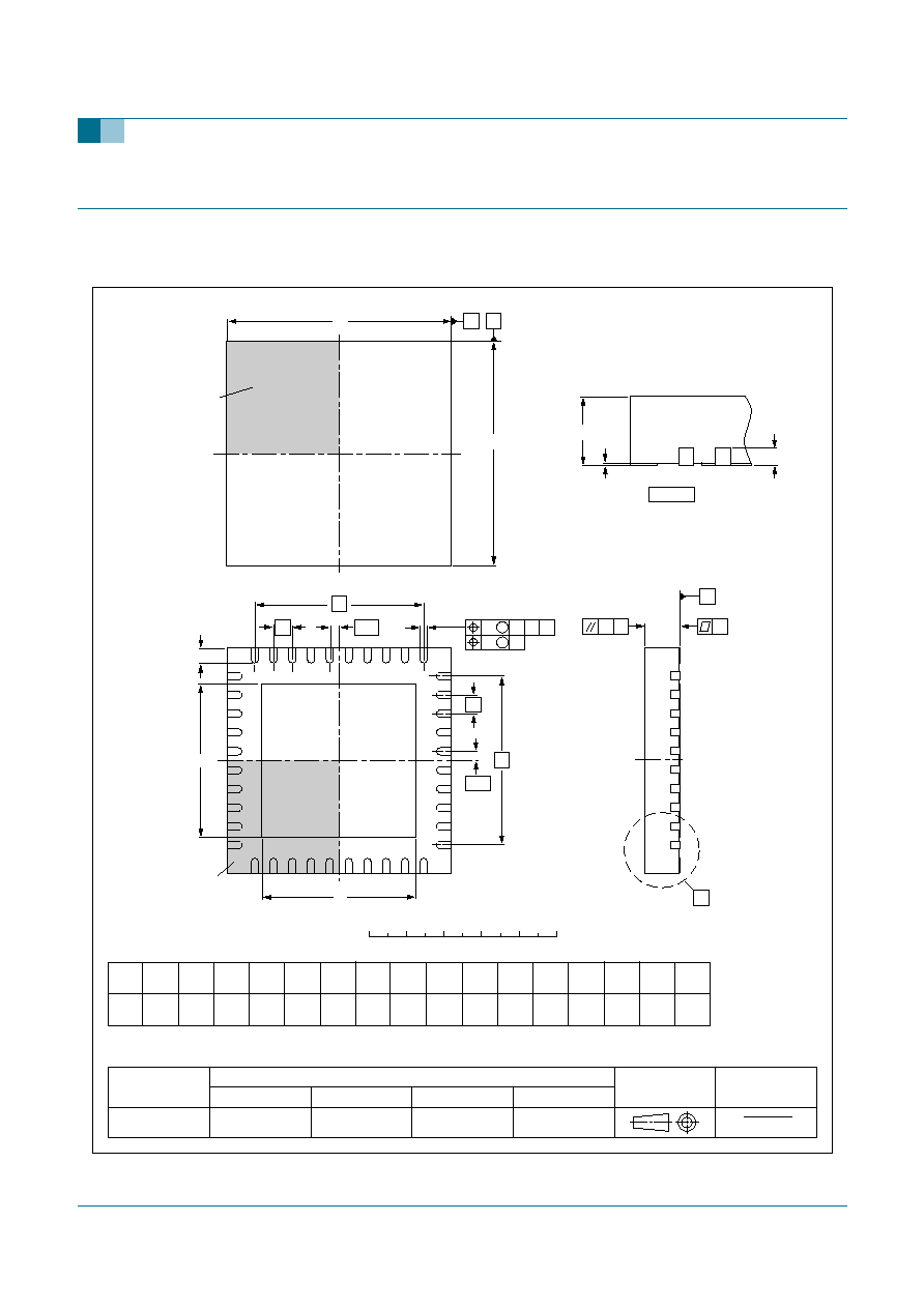
TEA5764HN_2
© Koninklijke Philips Electronics N.V. 2005. All rights reserved.
Product data sheet
Rev. 02 -- 9 August 2005
57 of 64
Philips Semiconductors
TEA5764HN
FM radio + RDS
17. Package outline
Fig 19. Package outline SOT618-1 (HVQFN40)
terminal 1
index area
0.5
1
A1
Eh
b
UNIT
y
e
0.2
c
REFERENCES
OUTLINE
VERSION
EUROPEAN
PROJECTION
ISSUE DATE
IEC
JEDEC
JEITA
mm
6.1
5.9
Dh
4.25
3.95
y1
6.1
5.9
4.25
3.95
e1
4.5
e2
4.5
0.30
0.18
0.05
0.00
0.05
0.1
DIMENSIONS (mm are the original dimensions)
SOT618-1
MO-220
- - -
- - -
0.5
0.3
L
0.1
v
0.05
w
0
2.5
5 mm
scale
SOT618-1
HVQFN40: plastic thermal enhanced very thin quad flat package; no leads;
40 terminals; body 6 x 6 x 0.85 mm
A
(1)
max.
A
A1
c
detail X
y
y1 C
e
L
Eh
Dh
e
e1
b
11
20
40
31
30
21
10
1
X
D
E
C
B
A
e2
01-08-08
02-10-22
terminal 1
index area
1/2
e
1/2
e
A
C
C
B
v
M
w
M
Note
1. Plastic or metal protrusions of 0.075 mm maximum per side are not included.
D
(1)
E
(1)

TEA5764HN_2
© Koninklijke Philips Electronics N.V. 2005. All rights reserved.
Product data sheet
Rev. 02 -- 9 August 2005
58 of 64
Philips Semiconductors
TEA5764HN
FM radio + RDS
18. Soldering
18.1 Introduction to soldering surface mount packages
This text gives a very brief insight to a complex technology. A more in-depth account of
soldering ICs can be found in our
Data Handbook IC26; Integrated Circuit Packages
(document order number 9398 652 90011).
There is no soldering method that is ideal for all surface mount IC packages. Wave
soldering can still be used for certain surface mount ICs, but it is not suitable for fine pitch
SMDs. In these situations reflow soldering is recommended.
18.2 Reflow soldering
Reflow soldering requires solder paste (a suspension of fine solder particles, flux and
binding agent) to be applied to the printed-circuit board by screen printing, stencilling or
pressure-syringe dispensing before package placement. Driven by legislation and
environmental forces the worldwide use of lead-free solder pastes is increasing.
Several methods exist for reflowing; for example, convection or convection/infrared
heating in a conveyor type oven. Throughput times (preheating, soldering and cooling)
vary between 100 seconds and 200 seconds depending on heating method.
Typical reflow peak temperatures range from 215
∞
C to 270
∞
C depending on solder paste
material. The top-surface temperature of the packages should preferably be kept:
∑
below 225
∞
C (SnPb process) or below 245
∞
C (Pb-free process)
≠ for all BGA, HTSSON..T and SSOP..T packages
≠ for packages with a thickness
2.5 mm
≠ for packages with a thickness < 2.5 mm and a volume
350 mm
3
so called
thick/large packages.
∑
below 240
∞
C (SnPb process) or below 260
∞
C (Pb-free process) for packages with a
thickness < 2.5 mm and a volume < 350 mm
3
so called small/thin packages.
Moisture sensitivity precautions, as indicated on packing, must be respected at all times.
18.3 Wave soldering
Conventional single wave soldering is not recommended for surface mount devices
(SMDs) or printed-circuit boards with a high component density, as solder bridging and
non-wetting can present major problems.
To overcome these problems the double-wave soldering method was specifically
developed.
If wave soldering is used the following conditions must be observed for optimal results:
∑
Use a double-wave soldering method comprising a turbulent wave with high upward
pressure followed by a smooth laminar wave.
∑
For packages with leads on two sides and a pitch (e):
≠ larger than or equal to 1.27 mm, the footprint longitudinal axis is preferred to be
parallel to the transport direction of the printed-circuit board;

TEA5764HN_2
© Koninklijke Philips Electronics N.V. 2005. All rights reserved.
Product data sheet
Rev. 02 -- 9 August 2005
59 of 64
Philips Semiconductors
TEA5764HN
FM radio + RDS
≠ smaller than 1.27 mm, the footprint longitudinal axis must be parallel to the
transport direction of the printed-circuit board.
The footprint must incorporate solder thieves at the downstream end.
∑
For packages with leads on four sides, the footprint must be placed at a 45
∞
angle to
the transport direction of the printed-circuit board. The footprint must incorporate
solder thieves downstream and at the side corners.
During placement and before soldering, the package must be fixed with a droplet of
adhesive. The adhesive can be applied by screen printing, pin transfer or syringe
dispensing. The package can be soldered after the adhesive is cured.
Typical dwell time of the leads in the wave ranges from 3 seconds to 4 seconds at 250
∞
C
or 265
∞
C, depending on solder material applied, SnPb or Pb-free respectively.
A mildly-activated flux will eliminate the need for removal of corrosive residues in most
applications.
18.4 Manual soldering
Fix the component by first soldering two diagonally-opposite end leads. Use a low voltage
(24 V or less) soldering iron applied to the flat part of the lead. Contact time must be
limited to 10 seconds at up to 300
∞
C.
When using a dedicated tool, all other leads can be soldered in one operation within
2 seconds to 5 seconds between 270
∞
C and 320
∞
C.
18.5 Package related soldering information
[1]
For more detailed information on the BGA packages refer to the
(LF)BGA Application Note (AN01026);
order a copy from your Philips Semiconductors sales office.
[2]
All surface mount (SMD) packages are moisture sensitive. Depending upon the moisture content, the
maximum temperature (with respect to time) and body size of the package, there is a risk that internal or
external package cracks may occur due to vaporization of the moisture in them (the so called popcorn
effect). For details, refer to the Drypack information in the
Data Handbook IC26; Integrated Circuit
Packages; Section: Packing Methods.
[3]
These transparent plastic packages are extremely sensitive to reflow soldering conditions and must on no
account be processed through more than one soldering cycle or subjected to infrared reflow soldering with
peak temperature exceeding 217
∞
C
±
10
∞
C measured in the atmosphere of the reflow oven. The package
body peak temperature must be kept as low as possible.
Table 50:
Suitability of surface mount IC packages for wave and reflow soldering methods
Package
[1]
Soldering method
Wave
Reflow
[2]
BGA, HTSSON..T
[3]
, LBGA, LFBGA, SQFP,
SSOP..T
[3]
, TFBGA, VFBGA, XSON
not suitable
suitable
DHVQFN, HBCC, HBGA, HLQFP, HSO, HSOP,
HSQFP, HSSON, HTQFP, HTSSOP, HVQFN,
HVSON, SMS
not suitable
[4]
suitable
PLCC
[5]
, SO, SOJ
suitable
suitable
LQFP, QFP, TQFP
not recommended
[5] [6]
suitable
SSOP, TSSOP, VSO, VSSOP
not recommended
[7]
suitable
CWQCCN..L
[8]
, PMFP
[9]
, WQCCN..L
[8]
not suitable
not suitable

TEA5764HN_2
© Koninklijke Philips Electronics N.V. 2005. All rights reserved.
Product data sheet
Rev. 02 -- 9 August 2005
60 of 64
Philips Semiconductors
TEA5764HN
FM radio + RDS
[4]
These packages are not suitable for wave soldering. On versions with the heatsink on the bottom side, the
solder cannot penetrate between the printed-circuit board and the heatsink. On versions with the heatsink
on the top side, the solder might be deposited on the heatsink surface.
[5]
If wave soldering is considered, then the package must be placed at a 45
∞
angle to the solder wave
direction. The package footprint must incorporate solder thieves downstream and at the side corners.
[6]
Wave soldering is suitable for LQFP, QFP and TQFP packages with a pitch (e) larger than 0.8 mm; it is
definitely not suitable for packages with a pitch (e) equal to or smaller than 0.65 mm.
[7]
Wave soldering is suitable for SSOP, TSSOP, VSO and VSSOP packages with a pitch (e) equal to or larger
than 0.65 mm; it is definitely not suitable for packages with a pitch (e) equal to or smaller than 0.5 mm.
[8]
Image sensor packages in principle should not be soldered. They are mounted in sockets or delivered
pre-mounted on flex foil. However, the image sensor package can be mounted by the client on a flex foil by
using a hot bar soldering process. The appropriate soldering profile can be provided on request.
[9]
Hot bar soldering or manual soldering is suitable for PMFP packages.

Philips Semiconductors
TEA5764HN
FM radio + RDS
TEA5764HN_2
© Koninklijke Philips Electronics N.V. 2005. All rights reserved.
Product data sheet
Rev. 02 -- 9 August 2005
61 of 64
19. Revision history
Table 51:
Revision history
Document ID
Release date
Data sheet status
Change notice
Doc. number
Supersedes
TEA5764HN_2
20050809
Product data sheet
-
-
TEA5764HN_1
Modifications:
∑
Specification status changed from objective data sheet to product data sheet.
TEA5764HN_1
20050707
Objective data sheet
-
9397 750 13453
-

Philips Semiconductors
TEA5764HN
FM radio + RDS
TEA5764HN_2
© Koninklijke Philips Electronics N.V. 2005. All rights reserved.
Product data sheet
Rev. 02 -- 9 August 2005
62 of 64
20. Data sheet status
[1]
Please consult the most recently issued data sheet before initiating or completing a design.
[2]
The product status of the device(s) described in this data sheet may have changed since this data sheet was published. The latest information is available on the Internet at
URL http://www.semiconductors.philips.com.
[3]
For data sheets describing multiple type numbers, the highest-level product status determines the data sheet status.
21. Definitions
Short-form specification -- The data in a short-form specification is
extracted from a full data sheet with the same type number and title. For
detailed information see the relevant data sheet or data handbook.
Limiting values definition -- Limiting values given are in accordance with
the Absolute Maximum Rating System (IEC 60134). Stress above one or
more of the limiting values may cause permanent damage to the device.
These are stress ratings only and operation of the device at these or at any
other conditions above those given in the Characteristics sections of the
specification is not implied. Exposure to limiting values for extended periods
may affect device reliability.
Application information -- Applications that are described herein for any
of these products are for illustrative purposes only. Philips Semiconductors
make no representation or warranty that such applications will be suitable for
the specified use without further testing or modification.
22. Disclaimers
Life support -- These products are not designed for use in life support
appliances, devices, or systems where malfunction of these products can
reasonably be expected to result in personal injury. Philips Semiconductors
customers using or selling these products for use in such applications do so
at their own risk and agree to fully indemnify Philips Semiconductors for any
damages resulting from such application.
Right to make changes -- Philips Semiconductors reserves the right to
make changes in the products - including circuits, standard cells, and/or
software - described or contained herein in order to improve design and/or
performance. When the product is in full production (status `Production'),
relevant changes will be communicated via a Customer Product/Process
Change Notification (CPCN). Philips Semiconductors assumes no
responsibility or liability for the use of any of these products, conveys no
license or title under any patent, copyright, or mask work right to these
products, and makes no representations or warranties that these products are
free from patent, copyright, or mask work right infringement, unless otherwise
specified.
23. Trademarks
Notice -- All referenced brands, product names, service names and
trademarks are the property of their respective owners.
I
2
C-bus -- wordmark and logo are trademarks of Koninklijke Philips
Electronics N.V.
24. Contact information
For additional information, please visit: http://www.semiconductors.philips.com
For sales office addresses, send an email to: sales.addresses@www.semiconductors.philips.com
Level
Data sheet status
[1]
Product status
[2] [3]
Definition
I
Objective data
Development
This data sheet contains data from the objective specification for product development. Philips
Semiconductors reserves the right to change the specification in any manner without notice.
II
Preliminary data
Qualification
This data sheet contains data from the preliminary specification. Supplementary data will be published
at a later date. Philips Semiconductors reserves the right to change the specification without notice, in
order to improve the design and supply the best possible product.
III
Product data
Production
This data sheet contains data from the product specification. Philips Semiconductors reserves the
right to make changes at any time in order to improve the design, manufacturing and supply. Relevant
changes will be communicated via a Customer Product/Process Change Notification (CPCN).

Philips Semiconductors
TEA5764HN
FM radio + RDS
TEA5764HN_2
© Koninklijke Philips Electronics N.V. 2005. All rights reserved.
Product data sheet
Rev. 02 -- 9 August 2005
63 of 64
continued >>
25. Contents
1
General description . . . . . . . . . . . . . . . . . . . . . . 1
2
Features . . . . . . . . . . . . . . . . . . . . . . . . . . . . . . . 1
3
Applications . . . . . . . . . . . . . . . . . . . . . . . . . . . . 2
4
Quick reference data . . . . . . . . . . . . . . . . . . . . . 2
5
Ordering information . . . . . . . . . . . . . . . . . . . . . 3
6
Block diagram . . . . . . . . . . . . . . . . . . . . . . . . . . 4
7
Pinning information . . . . . . . . . . . . . . . . . . . . . . 5
7.1
Pinning . . . . . . . . . . . . . . . . . . . . . . . . . . . . . . . 5
7.2
Pin description . . . . . . . . . . . . . . . . . . . . . . . . . 5
8
Functional description . . . . . . . . . . . . . . . . . . . 6
8.1
Low noise RF amplifier . . . . . . . . . . . . . . . . . . 6
8.2
FM I/Q mixer . . . . . . . . . . . . . . . . . . . . . . . . . . . 6
8.3
VCO . . . . . . . . . . . . . . . . . . . . . . . . . . . . . . . . . 6
8.4
Crystal oscillator . . . . . . . . . . . . . . . . . . . . . . . . 7
8.5
PLL tuning system . . . . . . . . . . . . . . . . . . . . . . 7
8.6
Band limits . . . . . . . . . . . . . . . . . . . . . . . . . . . . 8
8.7
RF AGC . . . . . . . . . . . . . . . . . . . . . . . . . . . . . . 8
8.8
Local or long distance receive . . . . . . . . . . . . . 8
8.9
IF filter. . . . . . . . . . . . . . . . . . . . . . . . . . . . . . . . 8
8.10
FM demodulator . . . . . . . . . . . . . . . . . . . . . . . . 8
8.11
IF counter . . . . . . . . . . . . . . . . . . . . . . . . . . . . . 8
8.12
Voltage level generator and analog-to-digital
converter. . . . . . . . . . . . . . . . . . . . . . . . . . . . . . 9
8.13
Mute . . . . . . . . . . . . . . . . . . . . . . . . . . . . . . . . . 9
8.13.1
Soft mute . . . . . . . . . . . . . . . . . . . . . . . . . . . . . 9
8.13.2
Hard mute . . . . . . . . . . . . . . . . . . . . . . . . . . . . . 9
8.13.3
Audio frequency mute . . . . . . . . . . . . . . . . . . . . 9
8.14
MPX decoder . . . . . . . . . . . . . . . . . . . . . . . . . . 9
8.15
Signal dependent mono/stereo blend (stereo
noise cancellation) . . . . . . . . . . . . . . . . . . . . . 10
8.16
Software programmable port . . . . . . . . . . . . . 10
8.17
Standby mode. . . . . . . . . . . . . . . . . . . . . . . . . 10
8.18
Power-on reset . . . . . . . . . . . . . . . . . . . . . . . . 10
8.19
RDS/RBDS . . . . . . . . . . . . . . . . . . . . . . . . . . . 10
8.19.1
RDS/RBDS demodulator . . . . . . . . . . . . . . . . 10
8.19.2
RDS data and clock direct . . . . . . . . . . . . . . . 11
8.19.2.1
RDS/RBDS decoder . . . . . . . . . . . . . . . . . . . . 11
8.20
Audio pause detector . . . . . . . . . . . . . . . . . . . 11
8.21
Auto search and Preset mode . . . . . . . . . . . . 11
8.21.1
Search mode . . . . . . . . . . . . . . . . . . . . . . . . . 13
8.21.2
Preset mode . . . . . . . . . . . . . . . . . . . . . . . . . . 13
8.21.3
Auto high-side and low-side injection stop
switch . . . . . . . . . . . . . . . . . . . . . . . . . . . . . . . 14
8.21.4
Muting during search or preset . . . . . . . . . . . . 14
8.22
RDS update/alternative frequency jump . . . . . 14
8.22.1
Muting during RDS update . . . . . . . . . . . . . . . 15
9
Interrupt handling . . . . . . . . . . . . . . . . . . . . . . 16
9.1
Interrupt register. . . . . . . . . . . . . . . . . . . . . . . 16
9.1.1
Interrupt clearing . . . . . . . . . . . . . . . . . . . . . . 17
9.1.2
Timing . . . . . . . . . . . . . . . . . . . . . . . . . . . . . . 17
9.1.3
Reset . . . . . . . . . . . . . . . . . . . . . . . . . . . . . . . 17
9.1.4
Interrupt flags and behavior . . . . . . . . . . . . . . 19
9.1.4.1
Multiple interrupt events . . . . . . . . . . . . . . . . . 19
9.1.4.2
Data available flag . . . . . . . . . . . . . . . . . . . . . 19
9.1.4.3
RDS synchronization flag. . . . . . . . . . . . . . . . 19
9.1.4.4
IF frequency flag . . . . . . . . . . . . . . . . . . . . . . 20
9.1.4.5
RSSI threshold flag . . . . . . . . . . . . . . . . . . . . 20
9.1.4.6
Pause detection flag. . . . . . . . . . . . . . . . . . . . 21
9.1.4.7
Frequency ready flag . . . . . . . . . . . . . . . . . . . 22
9.1.4.8
Band limit flag. . . . . . . . . . . . . . . . . . . . . . . . . 23
9.2
Interrupt output. . . . . . . . . . . . . . . . . . . . . . . . 23
10
RDS data processing . . . . . . . . . . . . . . . . . . . 23
10.1
DAV-A processing mode. . . . . . . . . . . . . . . . . 24
10.2
DAV-B processing mode / fast PI search mode 25
10.3
DAV-C reduced processing mode . . . . . . . . . 26
10.4
Synchronization . . . . . . . . . . . . . . . . . . . . . . . 28
10.4.1
Conditions for synchronization . . . . . . . . . . . . 28
10.4.2
Data overflow . . . . . . . . . . . . . . . . . . . . . . . . . 29
10.5
RDS flag behavior during read action . . . . . . 30
10.6
Error detection and reporting . . . . . . . . . . . . . 31
10.7
RDS test modes . . . . . . . . . . . . . . . . . . . . . . . 31
10.8
Reading RDS data from the registers . . . . . . 31
11
I
2
C-bus interface . . . . . . . . . . . . . . . . . . . . . . . 31
11.1
Write and read mode . . . . . . . . . . . . . . . . . . . 31
11.2
Data transfer. . . . . . . . . . . . . . . . . . . . . . . . . . 32
11.3
Register map . . . . . . . . . . . . . . . . . . . . . . . . . 34
11.4
Byte description . . . . . . . . . . . . . . . . . . . . . . . 34
12
Limiting values . . . . . . . . . . . . . . . . . . . . . . . . 45
13
Thermal characteristics . . . . . . . . . . . . . . . . . 45
14
Static characteristics . . . . . . . . . . . . . . . . . . . 46
15
Dynamic characteristics . . . . . . . . . . . . . . . . . 47
16
Application information . . . . . . . . . . . . . . . . . 56
17
Package outline . . . . . . . . . . . . . . . . . . . . . . . . 57
18
Soldering . . . . . . . . . . . . . . . . . . . . . . . . . . . . . 58
18.1
Introduction to soldering surface mount
packages . . . . . . . . . . . . . . . . . . . . . . . . . . . . 58
18.2
Reflow soldering. . . . . . . . . . . . . . . . . . . . . . . 58
18.3
Wave soldering. . . . . . . . . . . . . . . . . . . . . . . . 58
18.4
Manual soldering . . . . . . . . . . . . . . . . . . . . . . 59
18.5
Package related soldering information . . . . . . 59
19
Revision history . . . . . . . . . . . . . . . . . . . . . . . 61
20
Data sheet status. . . . . . . . . . . . . . . . . . . . . . . 62

© Koninklijke Philips Electronics N.V. 2005
All rights are reserved. Reproduction in whole or in part is prohibited without the prior
written consent of the copyright owner. The information presented in this document does
not form part of any quotation or contract, is believed to be accurate and reliable and may
be changed without notice. No liability will be accepted by the publisher for any
consequence of its use. Publication thereof does not convey nor imply any license under
patent- or other industrial or intellectual property rights.
Date of release: 9 August 2005
Document number: TEA5764HN_2
Published in The Netherlands
Philips Semiconductors
TEA5764HN
FM radio + RDS
21
Definitions . . . . . . . . . . . . . . . . . . . . . . . . . . . . 62
22
Disclaimers . . . . . . . . . . . . . . . . . . . . . . . . . . . . 62
23
Trademarks. . . . . . . . . . . . . . . . . . . . . . . . . . . . 62
24
Contact information . . . . . . . . . . . . . . . . . . . . 62