 | –≠–ª–µ–∫—Ç—Ä–æ–Ω–Ω—ã–π –∫–æ–º–ø–æ–Ω–µ–Ω—Ç: TEA6101 | –°–∫–∞—á–∞—Ç—å:  PDF PDF  ZIP ZIP |

DATA SHEET
Objective specification
File under Integrated circuits, IC01
May 1992
INTEGRATED CIRCUITS
TEA6101/T
Antenna diversity circuit

May 1992
2
Philips Semiconductors
Objective specification
Antenna diversity circuit
TEA6101/T
FEATURES
∑
Ability to switch between up to four antennae
∑
Switching signal derived from two signals: the audio and
the level signals
∑
Floating switching threshold adjusts switching rate to
prevailing circumstances:
≠ increasing threshold due to excessive noise
≠ increasing threshold due to numerous level variations
∑
Memory for the most favourable antenna signal to
overcome unnecessary switching
∑
Signal-dependent `soft` muting circuit
∑
Mode selection to the first antenna receiving an AM
signal whilst the diversity system is reset.
APPLICATIONS
∑
Car radio receivers
∑
Mobile radio communications equipment
GENERAL DESCRIPTION
Intended for multi-antenna FM car radio reception
(antenna diversity system), the TEA6101/T selects the
most favourable signal from one of up to four antennae.
Founded upon audible signal disturbance the criteria are
derived from two signals: high frequency components (e.g.
spikes due to noise and multipath reception) and
variations in signal level as a result of multipath reception
or fluctuations in field strength.
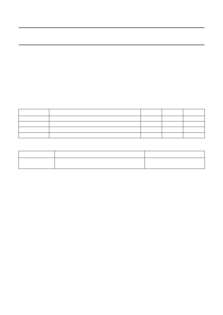
QUICK REFERENCE DATA
ORDERING INFORMATION
Notes
1. SOT102-1; 1996 September 10.
2. SOT163-1; 1996 September 10.
SYMBOL
PARAMETER
MIN.
TYP.
MAX.
UNIT
V
P
positive supply voltage
-
8.5
-
V
I
P
positive supply current
-
14
-
mA
V
I(p-p)
audio input voltage (peak-to-peak value)
-
-
3
V
I
os
antenna switch output current (source/sink)
-
-
7
mA
V
L
-
3 dB audio attenuation (soft mute)
-
1.45
-
V
T
amb
operating ambient temperature range
-
30
-
+85
∞
C
EXTENDED TYPE NUMBER
PACKAGE
PINS
PIN POSITION
MATERIAL
CODE
TEA6101
18
DIL
plastic
SOT102
(1)
TEA6101T
20
SO
plastic
SOT163A
(2)
May 1992
3
Philips Semiconductors
Objective specification
Antenna diversity circuit
TEA6101/T
This text is here in white to force landscape pages to be rotated correctly when browsing through the pdf in the Acrobat reader.This text is here in
_
white to force landscape pages to be rotated correctly when browsing through the pdf in the Acrobat reader.This text is here inThis text is here in
white to force landscape pages to be rotated correctly when browsing through the pdf in the Acrobat reader. white to force landscape pages to be ...
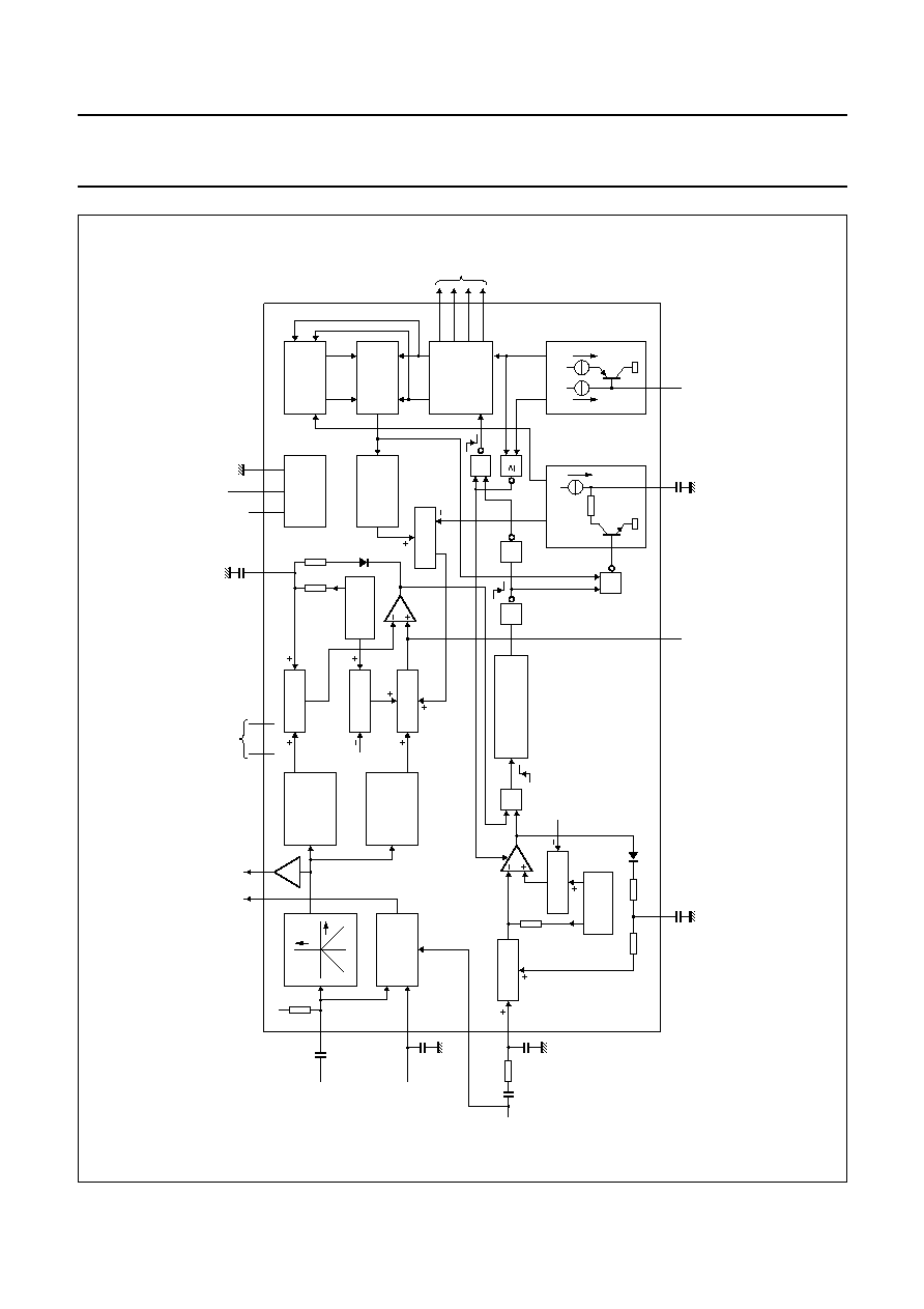
handbook, full pagewidth
MBA543 - 1
TEA6101T
VOLTAGE
REFERENCE
ADDER
ADDER
ADDER
100
R3
TIMING
MODE SELECT
MEMORY
COMPARATOR
4 - STAGE
JOHNSON
COUNTER
19
18
17
16
&
1
STABILIZER
OFFSET
12
k
R1
1.5
k
LOW - PASS
FILTER
HIGH - PASS
FILTER
offset
voltage
V (min)
ADDER
&
&
&
&
Vref
VU
VI
3
MUTE
MONOSTABLE
MULTIVIBRATOR
offset
complete
stop
reset
reset
0.47
µ
F
audio input
33
nF
ADDER
ADDER
VOLTAGE
REFERENCE
33 k
1.5 k
1
µ
F
R2
14
20
k
offset
voltage
20
k
3.6 V
delay soft mute
level input direct
3.3
nF
level input
via
capacitor
1
µ
F
7
5
6
4
8
11
10
13
9
1
20
12
15
2
ground
47 nF
level
averaging
test pin
memory
timing
control
to
antenna
switch
LOAD
reference
voltage
supply
noise
averaging
0.1
µ
F
not connected
audio output
modulus output
3.3 k
Fig.1 Block diagram.
May 1992
4
Philips Semiconductors
Objective specification
Antenna diversity circuit
TEA6101/T
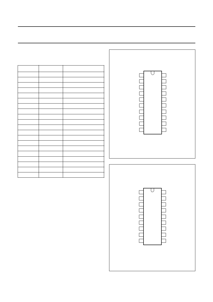
PINNING
The pin numbers given in parenthesis refer to the
TEA6101
SYMBOL
PIN
DESCRIPTION
V
P
1
(1)
positive supply
CTRL
2
(2)
control input
AUDIN
3
(3)
audio input
AUDOUT
4
(4)
audio output
LID
5
(5)
level input direct
LIC
6
(6)
level input via capacitor
DSM
7
(7)
delay soft mute
MODOUT
8
(8)
modulus output
V
ref
9
(9)
reference voltage
n.c.
10
-
not connected
n.c.
11
-
not connected
TEST
12
(10)
test pin
NOAV
13
(11)
noise averaging
LEAV
14
(12)
level averaging
MT
15
(13)
memory timing
OUT4
16
(14)
output 4
OUT3
17
(15)
output 3
OUT2
18
(16)
output 2
OUT1
19
(17)
output 1
GND
20
(18)
ground
handbook, halfpage
1
2
3
4
5
6
7
8
9
10
20
19
18
17
16
15
14
13
12
11
MBA542 - 1
n.c.
n.c.
TEA6101T
CTRL
AUDIN
AUDOUT
LID
LIC
DSM
MODOUT
GND
OUT1
OUT2
OUT3
OUT4
MT
LEAV
NOAV
TEST
VP
VREF
Fig.2 Pin configuration (TEA6101T).
handbook, halfpage
1
2
3
4
5
6
7
8
9
18
17
16
15
14
13
12
11
10
CTRL
AUDIN
AUDOUT
LID
LIC
DSM
MODOUT
MBA541 - 1
GND
OUT1
OUT2
OUT3
OUT4
MT
LEAV
NOAV
TEST
TEA6101
VP
VREF
Fig.3 Pin configuration (TEA6101).

May 1992
5
Philips Semiconductors
Objective specification
Antenna diversity circuit
TEA6101/T
FUNCTIONAL DESCRIPTION
Various forms of disturbance can affect signal reception in
car radio receivers:
∑
ignition interference produces spikes on the audio
signal. Switching to another antenna will be ineffective.
Strong ignition interference, however, will modulate the
antenna field strength. In this instance another antenna
possessing a directional pattern will suffer less
disturbance and switching would be appropriate.
∑
variation of antenna field strength due to travelling
through a zone of variable signal strength will result in a
variation in the signal level. Greater noise will be
apparent on the audio signal whilst the IF limiter is not
limiting. Switching to an alternative antenna input would
increase the signal strength.
∑
multipath reception occurs when a signal reaches the
antenna from two or more directions. Often the signals
will be of different phase. In certain circumstances the
sum of the reflected signals results in zero and a large
spike will be evident on the audio signal. It will then be
necessary to switch to an alternative antenna from
which the sum of the received signals will be different.
The criteria for an antenna diversity system are high
frequency components (spikes and noise) on the audio
signal in combination with variations in signal level.
Detection of spikes on the audio signal
A rectifier, high pass filter, low pass filter and a comparator
are used to detect spikes and noise on the audio signal
(see Fig.1). The negative spikes are detected by the
rectifier whilst a high pass filter removes the audio signal
to leave the high frequency signal components at the
negative input to the comparator. The signal at the positive
input to the comparator consists of an offset together with
an audio signal attenuated by the low pass filter. If the
amplitude of the spikes exceed that of the attenuated
audio plus offset, the output of the comparator is HIGH.
When the switching rate of the comparator is HIGH,
feedback increases the offset via the diode, the resistor
R1, and the 100 nF capacitor. The offset is decreased by
the 12 k
resistor and the 100 nF capacitor (pin 11 or 13).
The result is an offset based upon the comparator
switching rate, rapid to increase but slow to decrease,
therefore permitting only the largest spikes to trigger the
comparator (floating threshold).
Should high noise be apparent on the audio signal, the
offset is decreased by means of the rectifier and high pass
filter.
This will result in more frequent switching to an alternative
antenna whilst the result of the switching operation will be
less audible.
Detection of voltage level variation
A 1
µ
F input capacitor and 20 k
resistor remove the
absolute level voltage to leave only variations to be
detected. The level comparator output is HIGH when the
variations in level voltage are greater than the offset.
Similarly to the audio comparator; the feedback diode,
resistor R2, the 1
µ
F capacitor and the 33 k
resistor
cause the threshold level to float. During periods of high
activity the comparator thus switches only on the largest
variations.
Switching to an alternative antenna
When both the level and the audio comparator outputs are
HIGH, another output of the Johnson counter will be
selected. Since switching to an alternative antenna would
cause a disturbance of the audio and level signals the
monostable multivibrator will prohibit the counter from
selecting another antenna input for 21
µ
s.
Memory and timing
Approximately similar qualities of signal originating from
different antennae could result in unnecessary antenna
switching. This is prevented by appointing a priority
antenna. The selection of an antenna without priority
results in the audio offset being decreased by 1.2 V such
that the audio comparator will have a HIGH output voltage.
During the period of memory timing the offset increases
towards the normal offset value. Should level alterations
occur during this period another antenna will be selected.
If, however, the memory is timed-out without the
occurrence of signal variation, priority will be appointed to
the selected antenna. Thus a priority antenna will be
selected for the majority of the time during reception of
almost all similarly weak antenna signals.
Mute
A mute function should not precede the circuit. This
function is therefore assumed by the TEA6101. When
used in combination with the TEA6100 the 20 k
input of
the IF IC together with the 6 k
output resistor of the
TEA6101 cause an attenuation of 3 dB. The mute circuit
therefore has 3 dB amplification of level voltages in excess
of 2.75 V.
May 1992
6
Philips Semiconductors
Objective specification
Antenna diversity circuit
TEA6101/T
Mode selection
The diversity system is intended for FM reception. To
avoid an audible disturbance if it is used with an AM
system, the circuit can be reset. In the reset mode antenna
1 (pin 17 (19)) is selected and both comparators are
switched off to prevent pulses reaching the output.
For FM search tuning the diversity system may be similarly
disabled. The selected antenna will again be retained with
the comparators being inhibited.
Test pin
Although intended for test purposes the test pin can be
used to increase the audio offset (resistor from pin 10 (12)
to ground) or to change the compensation factor (resistor
between pin 8 (8) and 10 (12)). These modifications permit
the behaviour of the antenna switch to be adapted to
alternative IF amplifier IC's.
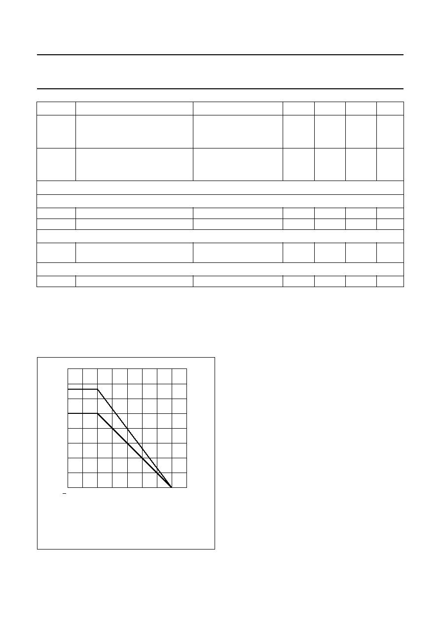
LIMITING VALUES
In accordance with the absolute maximum system (IEC 134)
THERMAL RESISTANCE
SYMBOL
PARAMETER
MIN.
MAX.
UNIT
V
P
positive supply voltage
0
12
V
P
tot
total power dissipation
-
see Fig.3
T
amb
operating ambient temperature range
-
30
+85
∞
C
T
stg
storage temperature range
-
55
+150
∞
C
SYMBOL
PARAMETER
THERMAL RESISTANCE
R
th c-a
from crystal to ambient (SOT102)
75 K/W
R
th c-a
from crystal to ambient (SOT163A)
150 K/W

May 1992
7
Philips Semiconductors
Objective specification
Antenna diversity circuit
TEA6101/T
DC CHARACTERISTICS
Measurements using application circuit (Fig 1) at T
amb
= 25
∞
C and V
P
= 8.5 V. Voltages with respect to pin 18 (20); pin
numbers in parenthesis refer to TEA6101T; all currents positive into the IC unless otherwise specified.
SYMBOL
PARAMETER
CONDITION
MIN.
TYP.
MAX.
UNIT
V
P
positive supply voltage
7.5
8.5
12
V
I
P
positive supply current
I
SO
= 0 mA
-
14
-
mA
P
tot
total power dissipation
-
119
-
mW
V
pins
voltage at pin:
1
(1)
-
8.5
-
V
2
(2)
-
7.8
-
V
3
(3)
-
3.6
-
V
4
(4)
-
5.4
-
V
5
(5)
-
0
-
V
6
(6)
-
5.3
-
V
7
(7)
-
0.6
-
V
8
(8)
-
5.2
-
V
9
(9)
-
5.4
-
V
-
(10)
-
n.c.
-
-
(11)
-
n.c.
-
10
(12)
-
5.1
-
V
11
(13)
-
5.4
-
V
12
(14)
-
5.3
-
V
13
(15)
-
0
-
V
14
(16)
-
0
-
V
15
(17)
-
0
-
V
16
(18)
-
0
-
V
17
(19)
-
7.5
-
V
18
(20)
-
0
-
V

May 1992
8
Philips Semiconductors
Objective specification
Antenna diversity circuit
TEA6101/T
AC CHARACTERISTICS
V
P
= 8.5 V; T
amb
= 25
∞
C; unless otherwise specified
SYMBOL
PARAMETER
CONDITIONS
MIN.
TYP.
MAX.
UNIT
Mute
S
OFT
M
UTE
(V
L
)
Z
I
input impedance (pin 3 (3))
-
20
-
k
MR
mute range
note 1
17
19.3
-
V
V
aud
/V
I
mute gain
V
L
= 2.75 V
-
2.7
-
dB
V
L
= 1.45 V
-
1
0.6
2
dB
H
ARD
M
UTE
(V
MUTE
)
V
mute
-
60 dB output attenuation
-
455
-
mV
+I
m
mute ON sink current
V
mute
= 1 V, V
L
= 0 V
-
370
-
µ
A
-
I
m
mute `OFF` source current
V
mute
= 0 V
3
-
-
µ
A
THD
total harmonic distortion
V
i
= 200 mV; V
L
= 2.5 V
-
0.09
-
%
V
I(p-p)
audio input voltage
(peak-to-peak value)
THD
>
10%
-
3
-
V
(S+N)/N
signal-to-noise ratio; measured with
dB(A) curve
V
aud
= 600 mV; 1 kHz;
V
L
= 3 V
-
95
-
dB
V
aud
/V
p
ripple rejection
note 2; 300 Hz; 100 mV;
V
L
= 2.5 V
28
32
-
dB
V
ref
output reference voltage
-
5.3
-
V
V
off1
audio comparator offset voltage
V
off1
= V
min
-
V
ap
with priority
-
+250
-
mV
with no priority
V
t
= 0 V
-
-
1100
-
mV
V
t
= 3 V
-
-
348
-
mV
Level comparator
V
ref
-
V
il
voltage for high comparator output
-
56
-
mV
t
monostable multivibrator time
period
started with both
comparator outputs HIGH
16
21
28
µ
s
Timing/memory
-
I
t
source current
-
30
-
µ
A
C
t
value delay capacitor
-
-
50
nF
T
t
timing duration
C
t
= 47 nF
-
6
-
ms
+I
t
reset current
V
t
= 3 V
-
17.7
-
mA
V
t
change of priority antenna
-
3.7
-
V
Antenna switch outputs
-
I
os
output source current
-
-
7
mA
+I
os
output sink current
-
-
7
mA
May 1992
9
Philips Semiconductors
Objective specification
Antenna diversity circuit
TEA6101/T
Notes to the AC characteristics
1.
2. When V
P
(pin 1 (1)) is filtered with R = 25
and C = 100
µ
F the ripple rejection becomes 46 dB
V
SO
selected output voltage
I
SO
=
-
10 mA
V
P
-
2 V
-
-
V
I
SO
= 0.5 mA
V
P
-
1 V
-
-
V
V
NSO
not selected output voltage
I
SO
= +10 mA
-
-
0.7
V
I
SO
= 0 mA
-
-
0.1
V
Mode selection
ENABLE
V
r
all functions active
-
-
1
V
-
I
r
input current
V
r
= 1 V
-
-
12
µ
A
RESET
(
ACTIVE AT OPEN INPUT
)
V
r
voltage at first antenna
(pin 17 (19))
4.2
-
V
P
V
STOP
V
r
keep selected antenna voltage
1.6
-
3.5
V
SYMBOL
PARAMETER
CONDITIONS
MIN.
TYP.
MAX.
UNIT
V
aud
aV
L
2.75V
=
(
)
V
aud
aV
L
0.1V
=
(
)
-----------------------------------------------------
(1) SOT102
(2) SOT163A
handbook, halfpage
25
25
75
175
2.0
1.5
0.5
0
1.0
MBA540 - 1
125
T amb ( C)
o
Ptot
(W)
(1)
(2)
0
Fig.4 Derating curve.

May 1992
10
Philips Semiconductors
Objective specification
Antenna diversity circuit
TEA6101/T
PACKAGE OUTLINES
REFERENCES
OUTLINE
VERSION
EUROPEAN
PROJECTION
ISSUE DATE
IEC
JEDEC
EIAJ
SOT102-1
93-10-14
95-01-23
UNIT
A
max.
1
2
b
1
(1)
(1)
(1)
b
2
c
D
E
e
M
Z
H
L
mm
DIMENSIONS (inch dimensions are derived from the original mm dimensions)
A
min.
A
max.
b
max.
w
M
E
e
1
1.40
1.14
0.53
0.38
0.32
0.23
21.8
21.4
6.48
6.20
3.9
3.4
0.254
2.54
7.62
8.25
7.80
9.5
8.3
0.85
4.7
0.51
3.7
inches
0.055
0.044
0.021
0.015
0.013
0.009
1.40
1.14
0.055
0.044
0.86
0.84
0.26
0.24
0.15
0.13
0.01
0.10
0.30
0.32
0.31
0.37
0.33
0.033
0.19
0.020
0.15
M
H
c
(e )
1
M
E
A
L
seating plane
A
1
w
M
b
1
b
2
e
D
A
2
Z
18
1
10
9
b
E
pin 1 index
0
5
10 mm
scale
Note
1. Plastic or metal protrusions of 0.25 mm maximum per side are not included.
DIP18: plastic dual in-line package; 18 leads (300 mil)
SOT102-1

May 1992
11
Philips Semiconductors
Objective specification
Antenna diversity circuit
TEA6101/T
UNIT
A
max.
A
1
A
2
A
3
b
p
c
D
(1)
E
(1)
(1)
e
H
E
L
L
p
Q
Z
y
w
v
REFERENCES
OUTLINE
VERSION
EUROPEAN
PROJECTION
ISSUE DATE
IEC
JEDEC
EIAJ
mm
inches
2.65
0.30
0.10
2.45
2.25
0.49
0.36
0.32
0.23
13.0
12.6
7.6
7.4
1.27
10.65
10.00
1.1
1.0
0.9
0.4
8
0
o
o
0.25
0.1
DIMENSIONS (inch dimensions are derived from the original mm dimensions)
Note
1. Plastic or metal protrusions of 0.15 mm maximum per side are not included.
1.1
0.4
SOT163-1
10
20
w
M
b
p
detail X
Z
e
11
1
D
y
0.25
075E04
MS-013AC
pin 1 index
0.10
0.012
0.004
0.096
0.089
0.019
0.014
0.013
0.009
0.51
0.49
0.30
0.29
0.050
1.4
0.055
0.419
0.394
0.043
0.039
0.035
0.016
0.01
0.25
0.01
0.004
0.043
0.016
0.01
0
5
10 mm
scale
X
A
A
1
A
2
H
E
L
p
Q
E
c
L
v
M
A
(A )
3
A
SO20: plastic small outline package; 20 leads; body width 7.5 mm
SOT163-1
95-01-24
97-05-22

May 1992
12
Philips Semiconductors
Objective specification
Antenna diversity circuit
TEA6101/T
SOLDERING
Introduction
There is no soldering method that is ideal for all IC
packages. Wave soldering is often preferred when
through-hole and surface mounted components are mixed
on one printed-circuit board. However, wave soldering is
not always suitable for surface mounted ICs, or for
printed-circuits with high population densities. In these
situations reflow soldering is often used.
This text gives a very brief insight to a complex technology.
A more in-depth account of soldering ICs can be found in
our
"IC Package Databook" (order code 9398 652 90011).
DIP
S
OLDERING BY DIPPING OR BY WAVE
The maximum permissible temperature of the solder is
260
∞
C; solder at this temperature must not be in contact
with the joint for more than 5 seconds. The total contact
time of successive solder waves must not exceed
5 seconds.
The device may be mounted up to the seating plane, but
the temperature of the plastic body must not exceed the
specified maximum storage temperature (T
stg max
). If the
printed-circuit board has been pre-heated, forced cooling
may be necessary immediately after soldering to keep the
temperature within the permissible limit.
R
EPAIRING SOLDERED JOINTS
Apply a low voltage soldering iron (less than 24 V) to the
lead(s) of the package, below the seating plane or not
more than 2 mm above it. If the temperature of the
soldering iron bit is less than 300
∞
C it may remain in
contact for up to 10 seconds. If the bit temperature is
between 300 and 400
∞
C, contact may be up to 5 seconds.
SO
R
EFLOW SOLDERING
Reflow soldering techniques are suitable for all SO
packages.
Reflow soldering requires solder paste (a suspension of
fine solder particles, flux and binding agent) to be applied
to the printed-circuit board by screen printing, stencilling or
pressure-syringe dispensing before package placement.
Several techniques exist for reflowing; for example,
thermal conduction by heated belt. Dwell times vary
between 50 and 300 seconds depending on heating
method. Typical reflow temperatures range from
215 to 250
∞
C.
Preheating is necessary to dry the paste and evaporate
the binding agent. Preheating duration: 45 minutes at
45
∞
C.
W
AVE SOLDERING
Wave soldering techniques can be used for all SO
packages if the following conditions are observed:
∑
A double-wave (a turbulent wave with high upward
pressure followed by a smooth laminar wave) soldering
technique should be used.
∑
The longitudinal axis of the package footprint must be
parallel to the solder flow.
∑
The package footprint must incorporate solder thieves at
the downstream end.
During placement and before soldering, the package must
be fixed with a droplet of adhesive. The adhesive can be
applied by screen printing, pin transfer or syringe
dispensing. The package can be soldered after the
adhesive is cured.
Maximum permissible solder temperature is 260
∞
C, and
maximum duration of package immersion in solder is
10 seconds, if cooled to less than 150
∞
C within
6 seconds. Typical dwell time is 4 seconds at 250
∞
C.
A mildly-activated flux will eliminate the need for removal
of corrosive residues in most applications.
R
EPAIRING SOLDERED JOINTS
Fix the component by first soldering two diagonally-
opposite end leads. Use only a low voltage soldering iron
(less than 24 V) applied to the flat part of the lead. Contact
time must be limited to 10 seconds at up to 300
∞
C. When
using a dedicated tool, all other leads can be soldered in
one operation within 2 to 5 seconds between
270 and 320
∞
C.

May 1992
13
Philips Semiconductors
Objective specification
Antenna diversity circuit
TEA6101/T
DEFINITIONS
LIFE SUPPORT APPLICATIONS
These products are not designed for use in life support appliances, devices, or systems where malfunction of these
products can reasonably be expected to result in personal injury. Philips customers using or selling these products for
use in such applications do so at their own risk and agree to fully indemnify Philips for any damages resulting from such
improper use or sale.
Data sheet status
Objective specification
This data sheet contains target or goal specifications for product development.
Preliminary specification
This data sheet contains preliminary data; supplementary data may be published later.
Product specification
This data sheet contains final product specifications.
Limiting values
Limiting values given are in accordance with the Absolute Maximum Rating System (IEC 134). Stress above one or
more of the limiting values may cause permanent damage to the device. These are stress ratings only and operation
of the device at these or at any other conditions above those given in the Characteristics sections of the specification
is not implied. Exposure to limiting values for extended periods may affect device reliability.
Application information
Where application information is given, it is advisory and does not form part of the specification.