 | –≠–ª–µ–∫—Ç—Ä–æ–Ω–Ω—ã–π –∫–æ–º–ø–æ–Ω–µ–Ω—Ç: TEA6300 | –°–∫–∞—á–∞—Ç—å:  PDF PDF  ZIP ZIP |
Document Outline
- GENERAL DESCRIPTION
- QUICK REFERENCE DATA
- PACKAGE OUTLINES
- PINNING
- FUNCTIONAL DESCRIPTION
- RATINGS
- CHARACTERISTICS
- I 2 C-BUS FORMAT
- APPLICATION INFORMATION
- PACKAGE OUTLINES
- SOLDERING
- DEFINITIONS
- LIFE SUPPORT APPLICATIONS

DATA SHEET
Product specification
File under Integrated Circuits, IC01
May 1990
INTEGRATED CIRCUITS
TEA6300
TEA6300T
Sound fader control circuit
May 1990
2
Philips Semiconductors
Product specification
Sound fader control circuit
TEA6300
TEA6300T
GENERAL DESCRIPTION
The Sound Fader Control circuit (SOFAC) is an I
2
C-bus
controlled preamplifier for car radios.
Features
∑
Source selector for three stereo inputs
∑
Inputs and outputs for noise reduction circuits
∑
Volume and balance control; control range of 86 dB in
steps of 2 dB
∑
Bass and treble control from
+
15 dB (treble 12 dB)
to
-
12 dB in steps of 3 dB
∑
Fader control from 0 dB to
-
30 dB in steps of 2 dB
∑
Fast muting
∑
Low noise suitable for DOLBY* B and C NR (noise
reduction)
∑
Signal handling suitable for compact disc
∑
I
2
C-bus control for all functions
∑
ESD protected
QUICK REFERENCE DATA
* Dolby is a registered trademark of Dolby Laboratories Licensing Corporation, San Francisco, California (U.S.A.).
PACKAGE OUTLINES
28-lead dual in-line; plastic (SOT117); SOT117-1; 1996 August 15.
28-lead mini-pack; plastic (SO28; SOT136A); SOT136-1; 1996 August 15.
SYMBOL
PARAMETER
MIN.
TYP.
MAX.
UNIT
V
CC
Supply voltage
7,0
8,5
13,2
V
V
i(rms)
Input sensitivity for full power at the output stage
-
50
-
mV
V
i(rms)
Input signal handling
-
1,65
-
V
f
r
Frequency response
35
-
20 000
Hz
CS
Channel separation; f = 250 Hz to 10 kHz
70
92
-
dB
THD
Total harmonic distortion
-
0,05
-
%
(S
+
N)/N
Signal plus noise-to-noise ratio
-
80
-
dB
T
amb
Operating ambient temperature range
-
40
-
+
85
∞
C

May 1990
3
Philips Semiconductors
Product specification
Sound fader control circuit
TEA6300
TEA6300T
This text is here in white to force landscape pages to be rotated correctly when browsing through the pdf in the Acrobat reader.This text is here in
_
white to force landscape pages to be rotated correctly when browsing through the pdf in the Acrobat reader.This text is here inThis text is here in
white to force landscape pages to be rotated correctly when browsing through the pdf in the Acrobat reader. white to force landscape pages to be ...
Fig.1 Block diagram.

May 1990
4
Philips Semiconductors
Product specification
Sound fader control circuit
TEA6300
TEA6300T
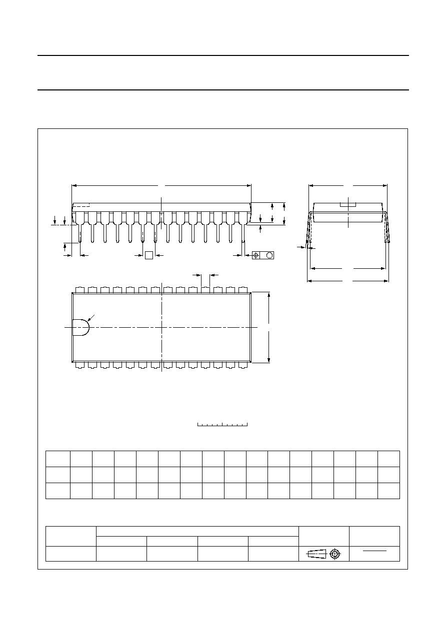
PINNING
1
SDA
serial data input/output (I
2
C-bus)
2
GNDB ground for I
2
C-bus terminals
3
QLR
output left rear
4
QLF
output left front
5
TL
treble control capacitor; left channel
6
BL1
bass control capacitor; left channel
7
BL0
bass control capacitor; left channel
8
INLA
input left source A
9
i.c.
internally connected
10
INLB
input left source B
11
ELFI
electronic filtering for supply
12
INLC
input left source C
13
QSL
output source selector left
14
INL
input left control part
15
INR
input right control part
16
QSR
output source selector right
17
INRC
input right source C
18
GND
ground
19
INRB
input right source B
20
V
ref
reference voltage (1/2 V
CC
)
21
INRA
input right source A
22
BRO
bass control capacitor; right channel
23
BR1
bass control capacitor; right channel
24
TR
treble control capacitor; right channel
25
QRF
output right front
26
QRR
output right rear
27
V
CC
supply voltage
28
SCL
serial clock input (I
2
C-bus)
Fig.2 Pinning diagram.

May 1990
5
Philips Semiconductors
Product specification
Sound fader control circuit
TEA6300
TEA6300T
FUNCTIONAL DESCRIPTION
The source selector selects three stereo channels
-
RF part (AM/FM), recorder and compact disc. As the outputs of the
source selector and the inputs of the main control part are available, additional circuits such as compander and equalizer
systems may be inserted into the signal path. The AC signal setting is performed by resistor chains in combination with
multi-input operational amplifiers. The advantage of this principle is the combination of low noise, low distortion and a
high dynamic range for the circuit.
The separate volume controls of the left and the right channel facilitate correct balance control. The range and balance
control is software programmable.
Because the TEA6300 has four outputs a low-level fader is included. The fader control is independent of the volume
control and an extra mute position is built in for the front, the rear or for all channels. The last function may be used for
muting during preset selection. An extra pop suppression circuit is built in for pop-free switching on and off. As all
switching and control functions are controllable via the two-wire I
2
C-bus, no external interface between the
microcomputer and the TEA6300 is required.
The on-chip power-on-reset sets the TEA6300 to the general mute mode.
RATINGS
Limiting values in accordance with the Absolute Maximum System (IEC 134)
SYMBOL
PARAMETER
MIN.
MAX.
UNIT
V
CC
Supply voltage (pin 27-18)
-
16
V
P
tot
Maximum power dissipation
-
1
W
T
stg
Storage temperature range
-
55
+
150
∞
C
T
amb
Operating ambient temperature range
-
40
+
85
∞
C

May 1990
6
Philips Semiconductors
Product specification
Sound fader control circuit
TEA6300
TEA6300T
CHARACTERISTICS
V
CC
= 8,5 V; R
S
= 600
; R
L
= 10 k
; f = 1 kHz; T
amb
= 25
∞
C; test circuit Fig.10; unless otherwise specified
SYMBOL
PARAMETER
MIN.
TYP.
MAX.
UNIT
V
CC
Supply voltage
7,0
8,5
13,2
V
I
CC
Supply current
-
26
-
mA
I
CC
Supply current at 8,5 V
-
-
33
mA
I
CC
Supply current at 13,2 V
-
-
44
mA
DC voltage
V
DC
inputs, outputs and reference
0,45
0,5
0,55
V
CC
Internal reference voltage (pin 20)
V
REF
V
ref
= 0,5 V
CC
-
4,25
-
V
Maximum voltage gain
G
v
bass and treble linear, fader off
19
20
21
dB
Output voltage level
V
o(rms)
for P
max
at the output stage
-
500
-
mV
V
o(rms)
for start of clipping
-
1000
-
mV
Input sensitivity
V
i(rms)
at V
o
= 500 mV
-
50
-
mV
Frequency response
bass and treble linear; roll-off
f
r
frequency
-
1 dB
35
-
20 000
Hz
Channel separation
G
v
= 0 dB; bass and treble linear;
CS
frequency range 250 Hz to 10 kHz
70
92
-
dB
Total harmonic distortion
frequency range 20 Hz to 12,5 kHz
THD
V
i
= 50 mV; G
v
= 20 dB
-
0,1
0,3
%
THD
V
i
= 500 mV; G
v
=
0 dB
-
0,05
0,2
%
THD
V
i
= 1,6 V;
G
v
=
-
10 dB
-
0,2
0,5
%
Ripple rejection
V
r(rms)
<
200 mV; G
v
= 0 dB;
bass and treble linear;
RR
100
at f = 100 Hz
-
70
-
dB
RR
range
at f = 40 Hz to 12,5 kHz
-
60
-
dB

May 1990
7
Philips Semiconductors
Product specification
Sound fader control circuit
TEA6300
TEA6300T
Signal plus noise-to-noise ratio
bass and treble linear; notes 1 and 2
CCIR 468-2 weighted; quasi peak
(S
+
N)/N
V
i
= 50 mV; V
o
= 46 mV; P
o
= 50 mW
-
65
-
dB
(S
+
N)/N
V
i
= 500 mV; V
o
= 45 mV; P
o
= 50 mW
-
67
-
dB
(S
+
N)/N
V
i
= 50 mV; V
o
= 200 mV; P
o
= 1 W
65
70
-
dB
(S
+
N)/N
V
i
= 500 mV; V
o
= 200 mV; P
o
= 1 W
65
78
-
dB
(S
+
N)/N
V
i
= 50 mV; V
o
= 500 mV; P
o
= 6 W
-
70
-
dB
(S
+
N)/N
V
i
= 500 mV; V
o
= 500 mV; P
o
= 6 W
-
85
-
dB
Noise output power
mute position, only contribution of
P
no
TEA6300; power amplifier for 25 W
-
-
10
nW
Crosstalk (20 log V
bus(p-p)
/V
o(rms)
)
between bus inputs and signal outputs
B
G
V
= 0 dB; bass and treble linear
-
110
-
dB
Source selector
Z
i
Input impedance
20
30
40
k
Z
o
Output impedance
-
-
100
R
L
Output load resistance
10
-
-
k
C
L
Output load capacity
0
-
200
pF
Input isolation
not selected source; frequency range
S
40 Hz to 12,5 kHz
-
80
-
dB
Voltage gain
G
v
R
L
10 k
-
0
-
dB
V
b int
/V
ref
Internal bias voltage ratio
-
1
-
Maximum input voltage level (RMS value)
V
i(rms)
THD < 0,5%
-
1,65
-
V
V
i(rms)
THD < 0,5%; V
CC
= 7,5 V
-
1,5
-
V
Total harmonic distortion
THD
V
i
= 500 mV; R
L
= 10 k
-
-
0,1
%
Noise output voltage
V
no
weighted CCIR 468-2, quasi peak
-
9
20
µ
V
DC offset voltage
V
o
between any inputs
-
-
10
mV
SYMBOL
PARAMETER
MIN.
TYP.
MAX.
UNIT

May 1990
8
Philips Semiconductors
Product specification
Sound fader control circuit
TEA6300
TEA6300T
Control part
Source selector disconnected,
source resistance 600
Z
i
Input impedance
35
50
65
k
Z
o
Output impedance
-
100
150
R
L
Output load resistance
5
-
-
k
C
L
Output load capacity
0
-
2500
pF
Maximum input voltage
THD < 0,5%; G
v
=
-
10 dB;
V
i(rms)
bass and treble linear
-
2,0
-
V
Noise output voltage
weighted acc CCIR 468-2, quasi-peak,
bass and treble linear, fader off
V
no
G
v
= 20 dB
-
110
220
µ
V
V
no
G
v
=
0 dB
-
25
50
µ
V
V
no
G
v
=
-
66 dB
-
19
38
µ
V
V
no
mute position
-
11
22
µ
V
Volume control
G
c
Continuous control range
-
86
-
dB
Step resolution
-
2
-
dB
Attenuator set error
G
a
(G
v
=
+
20 to
-
50 dB)
-
-
2
dB
Attenuator set error
G
a
(G
v
=
+
20 to
-
66 dB)
-
-
3
dB
Gain tracking error
balance in mid position,
G
t
bass and treble linear
-
-
2
dB
m
Mute attenuation
72
90
-
dB
DC step offset
Between any adjoining step
and any step to mute
G
v
= 0 to
-
66 dB
-
0,2
10
mV
G
v
= 20 to 0 dB
-
2
15
mV
In any treble and fader position
G
v
= 0 to
-
66 dB
-
-
10
mV
In any bass position
G
v
= 0 to
-
66 dB
-
-
20
mV
SYMBOL
PARAMETER
MIN.
TYP.
MAX.
UNIT
May 1990
9
Philips Semiconductors
Product specification
Sound fader control circuit
TEA6300
TEA6300T
Notes to the characteristics
1. The indicated values for output power assume a 6 W power amplifier with 20 dB gain, connected to the output of the
Bass control
Bass control range
G
b
f = 40 Hz; maximum boost
14
15
16
dB
G
b
f = 40 Hz; maximum attenuation
11
12
13
dB
Step resolution
-
3
-
dB
Step error
-
-
0,5
dB
Treble control
Treble control range
G
t
f = 15 kHz; maximum boost
11
12
13
dB
G
t
f = 15 kHz; maximum attenuation
11
12
13
dB
G
t
f > 15 kHz; maximum boost
-
-
15
dB
Step resolution
-
3
-
dB
Step error
-
-
0,5
dB
Fader control
Continuous attenuation
G
f
fader control range
-
30
-
dB
Step resolution
-
2
-
dB
Attenuator set error
-
-
1,5
dB
m
Mute attenuation
74
84
-
dB
Digital part
Bus terminals
Input voltage
V
IH
HIGH
3
-
12
V
V
IL
LOW
-
0,3
-
+
1,5
V
Input current
I
IH
HIGH
-
10
-
+
10
µ
A
I
IL
LOW
-
10
-
+
10
µ
A
V
OL
Output voltage LOW; I
L
= 3 mA
-
-
0,4
V
AC characteristics
In accordance with the I2C-bus specification
Power-on-Reset
When RESET is active the GMU (general mute)
bit is set and the I
2
C-bus receiver is in RESET
position
Increasing supply voltage
V
CC
start of reset
-
-
2,5
V
V
CC
end of reset
5,2
6,0
6,8
V
V
CC
Decreasing supply voltage; start of reset
4,2
5,0
5,8
V
SYMBOL
PARAMETER
MIN.
TYP.
MAX.
UNIT
May 1990
10
Philips Semiconductors
Product specification
Sound fader control circuit
TEA6300
TEA6300T
circuit. Signal-to-noise ratios exclude noise contribution of the power amplifier.
2. Signal-to-noise ratios on a CCIR 468-2 average meter reading are 4,5 dB better than on CCIR 468-2 quasi peak.
I
2
C-BUS FORMAT
If more than 1 byte of DATA is transmitted, then auto-increment of the subaddress is performed.
Table 1
I
2
C-bus; subaddress/data
S
SLAVE ADDRESS
A
SUBADDRESS
A
DATA
A
P
S
=
start condition
SUBADDRESS
=
see Table 1
SLAVE ADDRESS
=
1000 0000
DATA
=
see Table 1
A
=
acknowledge, generated by the slave
P
=
STOP condition
FUNCTION
SUBADDRESS
DATA
D7
D6
D5
D4
D3
D2
D1
D0
volume left
0 0 0 0 0 0 0 0
X
X
VL5
VL4
VL3
VL2
VL1
VL0
volume right
0 0 0 0 0 0 0 1
X
X
VR5
VR4
VR3
VR2
VR1
VR0
bass
0 0 0 0 0 0 1 0
X
X
X
X
BA3
BA2
BA1
BA0
treble
0 0 0 0 0 0 1 1
X
X
X
X
TR3
TR2
TR1
TR0
fader
0 0 0 0 0 1 0 0
X
X
MFN
FCH
FA3
FA2
FA1
FA0
switch
0 0 0 0 0 1 0 1
GMU
X
X
X
X
SCC
SCB
SCA
Function of the bits:
VL0 to VL5
volume control left
VR0 to VR5
volume control right
BA0 to BA3
bass control
TR0 to TR3
treble control
FA0 to FA3
fader control
FCH
select fader channel (front or rear)
MFN
mute control of the selected fader channel (front or rear)
SCA to SCC
source selector control
GMU
mute control (general mute)
for the outputs QLF, QLR, QRF and QRR
X
don't care bits (logic 1 during testing)

May 1990
11
Philips Semiconductors
Product specification
Sound fader control circuit
TEA6300
TEA6300T
Table 2
Bass setting
G
V
DATA
DB
BA3
BA2
BA1
BA0
+
15
1
1
1
1
+
15
1
1
1
0
+
15
1
1
0
1
+
15
1
1
0
0
+
12
1
0
1
1
+
9
1
0
1
0
+
6
1
0
0
1
+
3
1
0
0
0
0
0
1
1
1
-
3
0
1
1
0
-
6
0
1
0
1
-
9
0
1
0
0
-
12
0
0
1
1
-
12
0
0
1
0
-
12
0
0
0
1
-
12
0
0
0
0
Table 3
Treble setting
G
V
DATA
DB
TR3
TR2
TR1
TR0
+
12
1
1
1
1
+
12
1
1
1
0
+
12
1
1
0
1
+
12
1
1
0
0
+
12
1
0
1
1
+
9
1
0
1
0
+
6
1
0
0
1
+
3
1
0
0
0
0
0
1
1
1
-
3
0
1
1
0
-
6
0
1
0
1
-
9
0
1
0
0
-
12
0
0
1
1
-
12
0
0
1
0
-
12
0
0
0
1
-
12
0
0
0
0

May 1990
12
Philips Semiconductors
Product specification
Sound fader control circuit
TEA6300
TEA6300T
Table 4
Volume setting LEFT
G
V
DATA
DB
VL5
VL4
VL3
VL2
VL1
VL0
20
1
1
1
1
1
1
18
1
1
1
1
1
0
16
1
1
1
1
0
1
14
1
1
1
1
0
0
12
1
1
1
0
1
1
10
1
1
1
0
1
0
8
1
1
1
0
0
1
6
1
1
1
0
0
0
4
1
1
0
1
1
1
2
1
1
0
1
1
0
0
1
1
0
1
0
1
-
2
1
1
0
1
0
0
-
4
1
1
0
0
1
1
-
6
1
1
0
0
1
0
-
8
1
1
0
0
0
1
-
10
1
1
0
0
0
0
-
12
1
0
1
1
1
1
-
14
1
0
1
1
1
0
-
16
1
0
1
1
0
1
-
18
1
0
1
1
0
0
-
20
1
0
1
0
1
1
-
22
1
0
1
0
1
0
-
24
1
0
1
0
0
1
-
26
1
0
1
0
0
0
-
28
1
0
0
1
1
1
-
30
1
0
0
1
1
0
-
32
1
0
0
1
0
1
-
34
1
0
0
1
0
0
-
36
1
0
0
0
1
1
-
38
1
0
0
0
1
0
-
40
1
0
0
0
0
1
-
42
1
0
0
0
0
0
-
44
0
1
1
1
1
1
-
46
0
1
1
1
1
0
-
48
0
1
1
1
0
1
-
50
0
1
1
1
0
0
-
52
0
1
1
0
1
1
-
54
0
1
1
0
1
0
-
56
0
1
1
0
0
1
-
58
0
1
1
0
0
0
-
60
0
1
0
1
1
1
-
62
0
1
0
1
1
0
-
64
0
1
0
1
0
1
-
66
0
1
0
1
0
0
mute left
0
1
0
0
1
1
mute left
0
1
0
0
1
0
.
.
.
.
.
.
mute left
0
0
0
0
0
0
G
V
DATA
DB
VL5
VL4
VL3
VL2
VL1
VL0

May 1990
13
Philips Semiconductors
Product specification
Sound fader control circuit
TEA6300
TEA6300T
Table 5
Volume setting RIGHT
G
V
DATA
DB
VR5
VR4
VR3
VR2
VR1
VR0
20
1
1
1
1
1
1
18
1
1
1
1
1
0
16
1
1
1
1
0
1
14
1
1
1
1
0
0
12
1
1
1
0
1
1
10
1
1
1
0
1
0
8
1
1
1
0
0
1
6
1
1
1
0
0
0
4
1
1
0
1
1
1
2
1
1
0
1
1
0
0
1
1
0
1
0
1
-
2
1
1
0
1
0
0
-
4
1
1
0
0
1
1
-
6
1
1
0
0
1
0
-
8
1
1
0
0
0
1
-
10
1
1
0
0
0
0
-
12
1
0
1
1
1
1
-
14
1
0
1
1
1
0
-
16
1
0
1
1
0
1
-
18
1
0
1
1
0
0
-
20
1
0
1
0
1
1
-
22
1
0
1
0
1
0
-
24
1
0
1
0
0
1
-
26
1
0
1
0
0
0
-
28
1
0
0
1
1
1
-
30
1
0
0
1
1
0
-
32
1
0
0
1
0
1
-
34
1
0
0
1
0
0
-
36
1
0
0
0
1
1
-
38
1
0
0
0
1
0
-
40
1
0
0
0
0
1
-
42
1
0
0
0
0
0
-
44
0
1
1
1
1
1
-
46
0
1
1
1
1
0
-
48
0
1
1
1
0
1
-
50
0
1
1
1
0
0
-
52
0
1
1
0
1
1
-
54
0
1
1
0
1
0
-
56
0
1
1
0
0
1
-
58
0
1
1
0
0
0
-
60
0
1
0
1
1
1
-
62
0
1
0
1
1
0
-
64
0
1
0
1
0
1
-
66
0
1
0
1
0
0
mute right
0
1
0
0
1
1
mute right
0
1
0
0
1
0
.
.
.
.
.
.
mute right
0
0
0
0
0
0
G
V
DATA
DB
VR5
VR4
VR3
VR2
VR1
VR0

May 1990
14
Philips Semiconductors
Product specification
Sound fader control circuit
TEA6300
TEA6300T
Table 6
Fader function
SETTING
DATA
FRONT REAR
DB
DB
MFN
FCH
FA3
FA2
FA1
FA0
fader off
0
0
1
1
1
1
1
1
0
0
0
1
1
1
1
1
fader front
-
2
0
1
1
1
1
1
0
-
4
0
1
1
1
1
0
1
-
6
0
1
1
1
1
0
0
-
8
0
1
1
1
0
1
1
-
10
0
1
1
1
0
1
0
-
12
0
1
1
1
0
0
1
-
14
0
1
1
1
0
0
0
-
16
0
1
1
0
1
1
1
-
18
0
1
1
0
1
1
0
-
20
0
1
1
0
1
0
1
-
22
0
1
1
0
1
0
0
-
24
0
1
1
0
0
1
1
-
26
0
1
1
0
0
1
0
-
28
0
1
1
0
0
0
1
-
30
0
1
1
0
0
0
0
mute front
-
80
0
0
1
1
1
1
0
.
.
.
.
.
.
.
.
.
-
80
0
0
1
0
0
0
0
fader off
0
0
1
0
1
1
1
1
0
0
0
0
1
1
1
1
fader rear
0
-
2
1
0
1
1
1
0
0
-
4
1
0
1
1
0
1
0
-
6
1
0
1
1
0
0
0
-
8
1
0
1
0
1
1
0
-
10
1
0
1
0
1
0
0
-
12
1
0
1
0
0
1
0
-
14
1
0
1
0
0
0
0
-
16
1
0
0
1
1
1
0
-
18
1
0
0
1
1
0
0
-
20
1
0
0
1
0
1
0
-
22
1
0
0
1
0
0
0
-
24
1
0
0
0
1
1
0
-
26
1
0
0
0
1
0
0
-
28
1
0
0
0
0
1
0
-
30
1
0
0
0
0
0
mute rear
0
-
80
0
0
1
1
1
0
.
.
.
.
.
.
.
.
.
0
-
80
0
0
0
0
0
0
SETTING
DATA
FRONT REAR
DB
DB
MFN
FCH
FA3
FA2
FA1
FA0
Table 7
Selected inputs
SELECTED INPUTS
DATA
SCC
SCB
SCA
data not allowed
1
1
1
data not allowed
1
1
0
data not allowed
1
0
1
INLC, INRC
1
0
0
data not allowed
0
1
1
INLB, INRB
0
1
0
INLA, INRA
0
0
1
data not allowed
0
0
0
Table 8
Mute control
MUTE
DATA
REMARKS
CONTROL
GMU
active
1
outputs QLF, QLR
QRF and QRR are
muted
passive
0
no general mute
May 1990
15
Philips Semiconductors
Product specification
Sound fader control circuit
TEA6300
TEA6300T
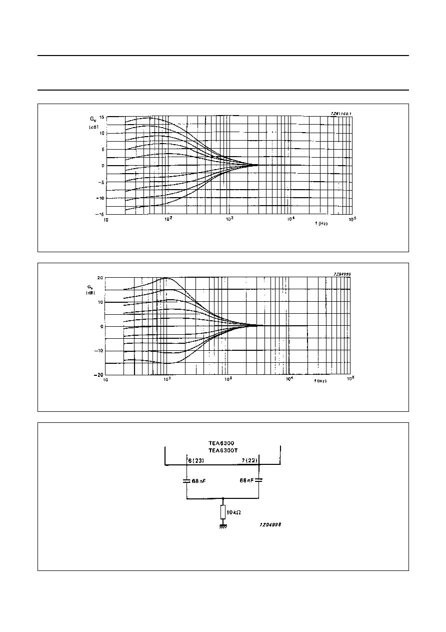
Fig.3 Bass control without T-pass filter.
Fig.4 Bass control with T-pass filter.
Fig.5 T-pass filter.
Pin numbers in parentheses refer to the bass control, right channel.

May 1990
16
Philips Semiconductors
Product specification
Sound fader control circuit
TEA6300
TEA6300T
Fig.6 Treble control.
Fig.7 Output noise voltage (CCIR 468-2 weighted: quasi peak).
May 1990
17
Philips Semiconductors
Product specification
Sound fader control circuit
TEA6300
TEA6300T
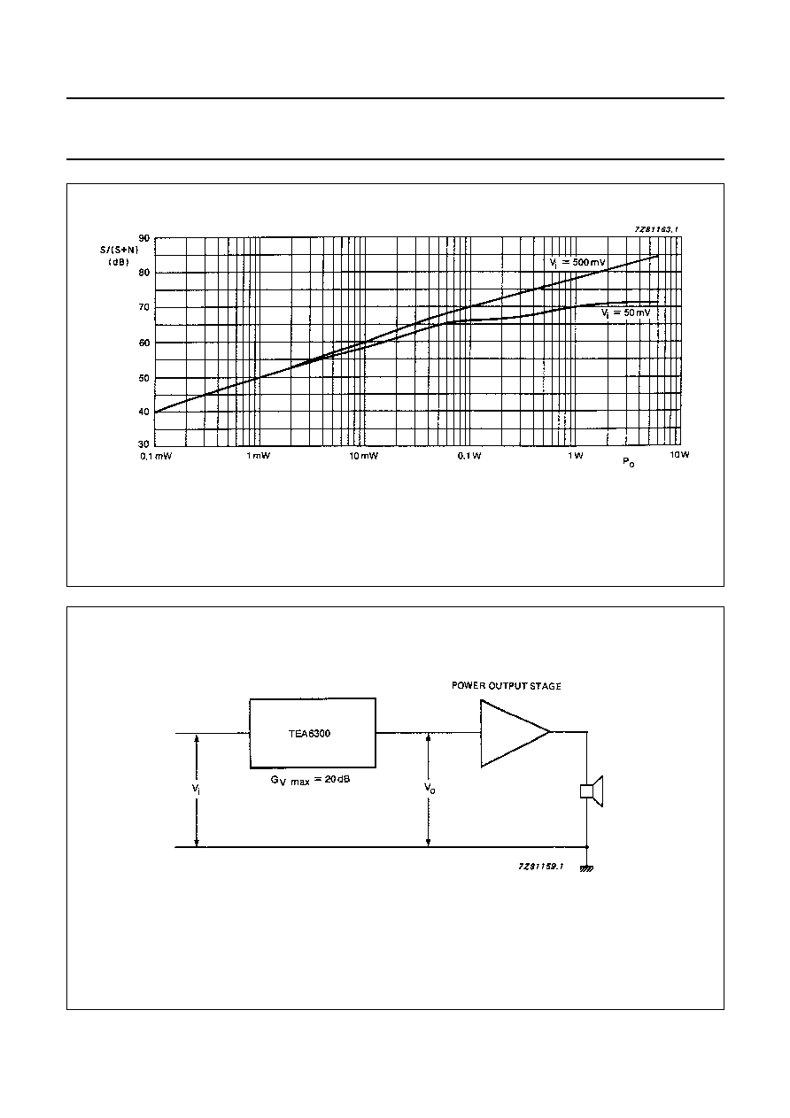
Fig.8
Signal-to-noise ratio (CCIT 468-2 weighted; quasi peak) with a 6 W power amplifier (gain 20 dB) without
noise contribution of the power amplifier (see Fig.9).
Fig.9 Recommended level diagram; V
i min
= 50 mV, V
o
= 500 mV for P
max
.
May 1990
18
Philips Semiconductors
Product specification
Sound fader control circuit
TEA6300
TEA6300T
APPLICATION INFORMATION
Fig.10 Test and application circuit.
May 1990
19
Philips Semiconductors
Product specification
Sound fader control circuit
TEA6300
TEA6300T
PACKAGE OUTLINES
UNIT
A
max.
1
2
b
1
(1)
(1)
(1)
c
D
E
w
e
M
H
L
REFERENCES
OUTLINE
VERSION
EUROPEAN
PROJECTION
ISSUE DATE
IEC
JEDEC
EIAJ
mm
inches
DIMENSIONS (inch dimensions are derived from the original mm dimensions)
SOT117-1
92-11-17
95-01-14
A
min.
A
max.
b
Z
max.
M
E
e
1
1.7
1.3
0.53
0.38
0.32
0.23
36.0
35.0
14.1
13.7
3.9
3.4
0.25
2.54
15.24
15.80
15.24
17.15
15.90
1.7
5.1
0.51
4.0
0.066
0.051
0.020
0.014
0.013
0.009
1.41
1.34
0.56
0.54
0.15
0.13
0.01
0.10
0.60
0.62
0.60
0.68
0.63
0.067
0.20
0.020
0.16
051G05
MO-015AH
M
H
c
(e )
1
M
E
A
L
seating plane
A
1
w
M
b
1
e
D
A
2
Z
28
1
15
14
b
E
pin 1 index
0
5
10 mm
scale
Note
1. Plastic or metal protrusions of 0.25 mm maximum per side are not included.
handbook, full pagewidth
DIP28: plastic dual in-line package; 28 leads (600 mil)
SOT117-1
May 1990
20
Philips Semiconductors
Product specification
Sound fader control circuit
TEA6300
TEA6300T
UNIT
A
max.
A
1
A
2
A
3
b
p
c
D
(1)
E
(1)
(1)
e
H
E
L
L
p
Q
Z
y
w
v
REFERENCES
OUTLINE
VERSION
EUROPEAN
PROJECTION
ISSUE DATE
IEC
JEDEC
EIAJ
mm
inches
2.65
0.30
0.10
2.45
2.25
0.49
0.36
0.32
0.23
18.1
17.7
7.6
7.4
1.27
10.65
10.00
1.1
1.0
0.9
0.4
8
0
o
o
0.25
0.1
DIMENSIONS (inch dimensions are derived from the original mm dimensions)
Note
1. Plastic or metal protrusions of 0.15 mm maximum per side are not included.
1.1
0.4
SOT136-1
X
14
28
w
M
A
A
1
A
2
b
p
D
H
E
L
p
Q
detail X
E
Z
c
L
v
M
A
e
15
1
(A )
3
A
y
0.25
075E06
MS-013AE
pin 1 index
0.10
0.012
0.004
0.096
0.089
0.019
0.014
0.013
0.009
0.71
0.69
0.30
0.29
0.050
1.4
0.055
0.419
0.394
0.043
0.039
0.035
0.016
0.01
0.25
0.01
0.004
0.043
0.016
0.01
0
5
10 mm
scale
SO28: plastic small outline package; 28 leads; body width 7.5 mm
SOT136-1
95-01-24
97-05-22

May 1990
21
Philips Semiconductors
Product specification
Sound fader control circuit
TEA6300
TEA6300T
SOLDERING
Introduction
There is no soldering method that is ideal for all IC
packages. Wave soldering is often preferred when
through-hole and surface mounted components are mixed
on one printed-circuit board. However, wave soldering is
not always suitable for surface mounted ICs, or for
printed-circuits with high population densities. In these
situations reflow soldering is often used.
This text gives a very brief insight to a complex technology.
A more in-depth account of soldering ICs can be found in
our
"IC Package Databook" (order code 9398 652 90011).
DIP
S
OLDERING BY DIPPING OR BY WAVE
The maximum permissible temperature of the solder is
260
∞
C; solder at this temperature must not be in contact
with the joint for more than 5 seconds. The total contact
time of successive solder waves must not exceed
5 seconds.
The device may be mounted up to the seating plane, but
the temperature of the plastic body must not exceed the
specified maximum storage temperature (T
stg max
). If the
printed-circuit board has been pre-heated, forced cooling
may be necessary immediately after soldering to keep the
temperature within the permissible limit.
R
EPAIRING SOLDERED JOINTS
Apply a low voltage soldering iron (less than 24 V) to the
lead(s) of the package, below the seating plane or not
more than 2 mm above it. If the temperature of the
soldering iron bit is less than 300
∞
C it may remain in
contact for up to 10 seconds. If the bit temperature is
between 300 and 400
∞
C, contact may be up to 5 seconds.
SO
R
EFLOW SOLDERING
Reflow soldering techniques are suitable for all SO
packages.
Reflow soldering requires solder paste (a suspension of
fine solder particles, flux and binding agent) to be applied
to the printed-circuit board by screen printing, stencilling or
pressure-syringe dispensing before package placement.
Several techniques exist for reflowing; for example,
thermal conduction by heated belt. Dwell times vary
between 50 and 300 seconds depending on heating
method. Typical reflow temperatures range from
215 to 250
∞
C.
Preheating is necessary to dry the paste and evaporate
the binding agent. Preheating duration: 45 minutes at
45
∞
C.
W
AVE SOLDERING
Wave soldering techniques can be used for all SO
packages if the following conditions are observed:
∑
A double-wave (a turbulent wave with high upward
pressure followed by a smooth laminar wave) soldering
technique should be used.
∑
The longitudinal axis of the package footprint must be
parallel to the solder flow.
∑
The package footprint must incorporate solder thieves at
the downstream end.
During placement and before soldering, the package must
be fixed with a droplet of adhesive. The adhesive can be
applied by screen printing, pin transfer or syringe
dispensing. The package can be soldered after the
adhesive is cured.
Maximum permissible solder temperature is 260
∞
C, and
maximum duration of package immersion in solder is
10 seconds, if cooled to less than 150
∞
C within
6 seconds. Typical dwell time is 4 seconds at 250
∞
C.
A mildly-activated flux will eliminate the need for removal
of corrosive residues in most applications.
R
EPAIRING SOLDERED JOINTS
Fix the component by first soldering two diagonally-
opposite end leads. Use only a low voltage soldering iron
(less than 24 V) applied to the flat part of the lead. Contact
time must be limited to 10 seconds at up to 300
∞
C. When
using a dedicated tool, all other leads can be soldered in
one operation within 2 to 5 seconds between
270 and 320
∞
C.

May 1990
22
Philips Semiconductors
Product specification
Sound fader control circuit
TEA6300
TEA6300T
DEFINITIONS
LIFE SUPPORT APPLICATIONS
These products are not designed for use in life support appliances, devices, or systems where malfunction of these
products can reasonably be expected to result in personal injury. Philips customers using or selling these products for
use in such applications do so at their own risk and agree to fully indemnify Philips for any damages resulting from such
improper use or sale.
Data sheet status
Objective specification
This data sheet contains target or goal specifications for product development.
Preliminary specification
This data sheet contains preliminary data; supplementary data may be published later.
Product specification
This data sheet contains final product specifications.
Limiting values
Limiting values given are in accordance with the Absolute Maximum Rating System (IEC 134). Stress above one or
more of the limiting values may cause permanent damage to the device. These are stress ratings only and operation
of the device at these or at any other conditions above those given in the Characteristics sections of the specification
is not implied. Exposure to limiting values for extended periods may affect device reliability.
Application information
Where application information is given, it is advisory and does not form part of the specification.