Document Outline
- FEATURES
- APPLICATIONS
- GENERAL DESCRIPTION
- QUICK REFERENCE DATA
- ORDERING INFORMATION
- BLOCK DIAGRAM
- PINNING
- I 2 C-BUS ORGANIZATION
- LIMITING VALUES
- HANDLING
- THERMAL CHARACTERISTICS
- DC CHARACTERISTICS
- AC CHARACTERISTICS
- INTERNAL PIN CONFIGURATION
- APPLICATION INFORMATION
- PACKAGE OUTLINES
- SOLDERING
- DEFINITIONS
- LIFE SUPPORT APPLICATIONS
- PURCHASE OF PHILIPS I 2 C COMPONENTS

DATA SHEET
Product specification
Supersedes data of September 1994
File under Integrated Circuits, IC01
1996 Jun 18
INTEGRATED CIRCUITS
TEA6810V; TEA6811V
Front-end and PLL synthesizers for
car radios
1996 Jun 18
2
Philips Semiconductors
Product specification
Front-end and PLL synthesizers for
car radios
TEA6810V; TEA6811V
FEATURES
∑
Synthesizer function which includes a Voltage
Controlled Oscillator (VCO), dividers, phase detector,
charge-pump and in-lock detector
∑
FM mixer with AGC
∑
AM RF amplifier with AGC
∑
AM mixer.
APPLICATIONS
∑
Car radios.
GENERAL DESCRIPTION
The TEA6810V and TEA6811V, together with TEA6821V
forms an AM/FM receiving concept for electronically tuned
car radios.
The TEA681xV is an FM/AM front-end with one local
synthesized oscillator for both AM and FM which is used
together with the TEA6821T in a double-conversion
concept. It delivers a first FM-IF of 72.2 MHz and, for
MW/LW, a first AM-IF of 10.7 MHz.
Minimum alignments are required due to wideband RF
inputs and the common AM/FM VCO.
High dynamic behaviour and minimum distortion is
obtained by a special RF input design combined with AGC.
High sensitivity is possible in combination with RF input
FETs.
Minimum interference is experienced due a to special
synthesizer loop design and ensuring that the I
2
C-bus is
inoperative in the locked-tuned condition.
The reference frequency for the synthesizer and the
I
2
C-bus information is delivered by the TEA6821V.
The programmable local/dx switch enables switching the
gain of the FM mixer from normal AGC control (FM dx) to
the forced 4th level of AGC (FM local).
QUICK REFERENCE DATA
ORDERING INFORMATION
SYMBOL
PARAMETER
CONDITIONS
MIN.
TYP.
MAX.
UNIT
V
CCA1
analog supply voltage (pin 2)
4.75
5.0
5.25
V
V
CCA2
analog supply voltage (pin 13)
8.1
8.5
8.9
V
V
AMant
AM AGC range
see Fig.4
0.3
-
6.0
V
V
FMant
FM AGC range
see Fig.5
10
-
600
mV
f
AMant
AM input frequency
0.144
-
22
MHz
f
FMant
FM input frequency
60
-
108
MHz
T
amb
operating ambient temperature
-
40
-
+85
∞
C
TYPE
NUMBER
PACKAGE
NAME
DESCRIPTION
VERSION
TEA6810V
VSO40
plastic very small outline package; 40 leads
SOT158-1
TEA6811V
VSO40
plastic very small outline package; 40 leads; face down
SOT158-2
1996
Jun
18
3
Philips Semiconductors
Product specification
Front-end and PLL synthesizers for
car radios
TEA6810V
; TEA681
1V
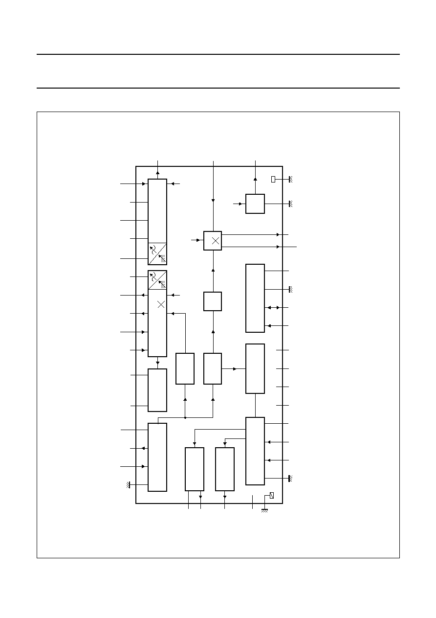
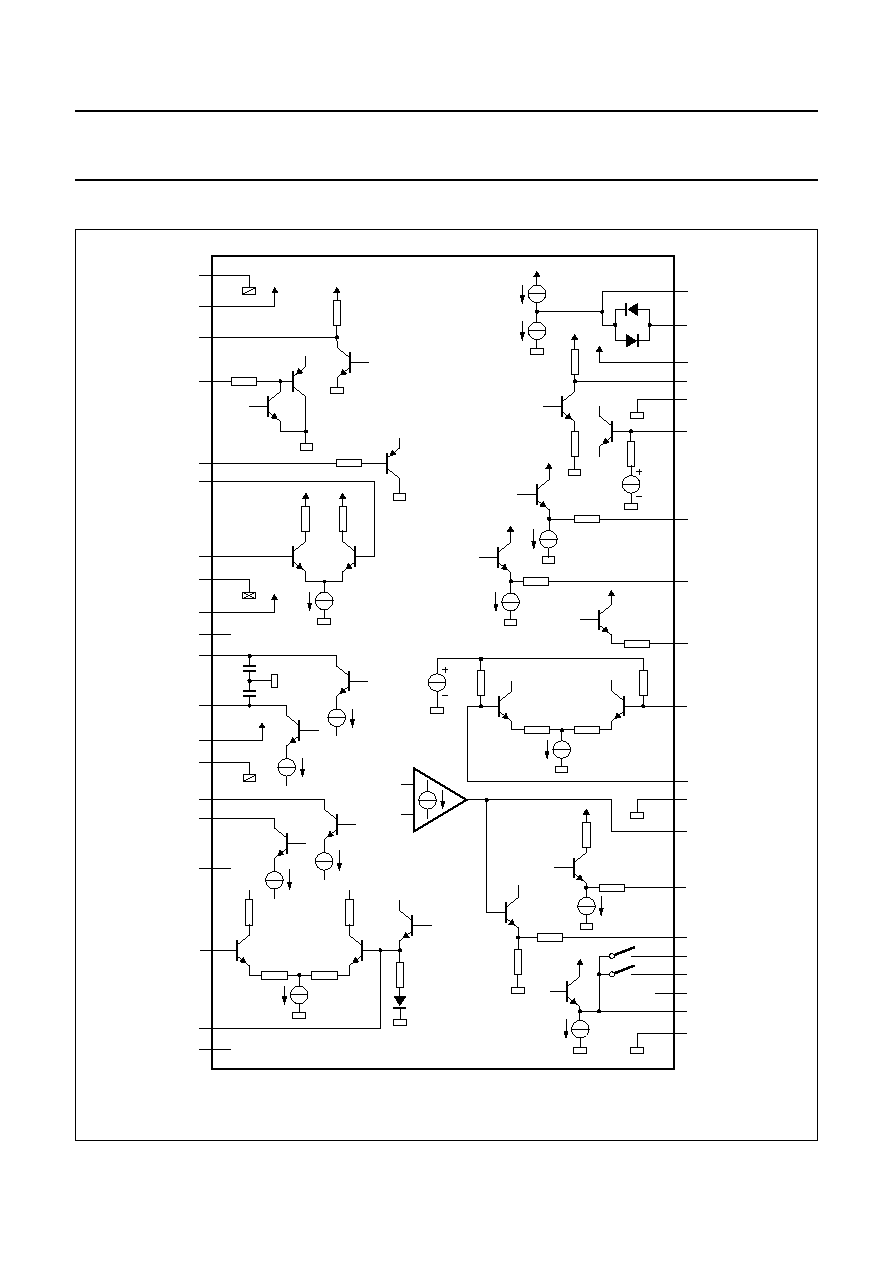
BLOCK DIAGRAM
n
dbook, full pagewidth
MGE727
AM/FM
OSCILLATOR
PIN DIODE
DRIVER
LOCK
DETECTOR
CHARGE
PUMP
PROGRAMME
DIVIDER N1
BAND
GAP
FM
AM
RF
AM/FM
AM/FM
AM/FM
TEA6810V
TEA6811V
AM/FM
BUFFER
OSCGND
OSCFDB
OSCTNK
IPIDIO
FMRFIP
FMRFIN
FMIFON
FMIFOP
AMPREC
AMSB2
AMSB1
AMPREI
FMAGCC
AMAGCC
VCCOSC
FMAGCref
BUFFER
I
2
C-BUS CONTROL
PHASE DETECTOR
N2
AM
36
35
37
38
34
32
30
31
11
12
33
27
28
25
24
26
AMPREO
AMMIN
Vref
22
18
19
15
9
8
4
5
20
10
23
17
2
7
6
1
AGND1
n.c.
n.c.
n.c.
n.c.
SCL
SDA
DGND
AMMOP
AMMON
AMMGND RFGND
VCCD
frefN
frefP VCCA1
VTUNE
VCCA2
CHPOUT
LCKDET
AGND2
14
13
3
40
39
16
21
29
Fig.1 Block diagram.

1996 Jun 18
4
Philips Semiconductors
Product specification
Front-end and PLL synthesizers for
car radios
TEA6810V; TEA6811V
PINNING
SYMBOL
PIN
(1)
DESCRIPTION
TEA6810
TEA6811
AGND1
1
1
analog ground 1
V
CCA1
2
2
analog supply voltage 1 (+5 V)
LCKDET
3
3
lock detector flag
SDA
4
4
serial data input/output; I
2
C-bus
SCL
5
5
serial clock input; I
2
C-bus
f
refN
6
6
reference frequency input from TEA6821 N-terminal
f
refP
7
7
reference frequency input from TEA6821 P-terminal
DGND
8
8
digital ground
V
CCD
9
9
digital supply voltage (+5 V)
n.c.
10
10
not connected
FMIFON
11
11
FM mixer negative output (72.2 MHz)
FMIFOP
12
12
FM mixer positive output (72.2 MHz)
V
CCA2
13
13
analog supply voltage 2 (+8.5 V)
AGND2
14
14
analog ground 2
AMMOP
15
15
AM mixer positive output (10.7 MHz)
AMMON
16
16
AM mixer negative output (10.7 MHz)
n.c.
17
17
not connected
AMMIN
18
18
AM mixer RF input
V
ref
19
19
reference voltage output from AM band gap
n.c.
20
20
not connected
AMMGND
21
21
AM mixer ground
AMPREO
22
22
AM preamplifier output
n.c.
23
23
not connected
AMSB1
24
24
AM feedback switch SB1
AMSB2
25
25
AM feedback switch SB2
AMPREI
26
26
AM preamplifier input
AMAGCC
27
27
AM AGC capacitor
AMPREC
28
28
AM preamplifier decoupling capacitor
RFGND
29
29
RF ground
FMRFIP
30
30
RF positive input for FM mixer
FMRFIN
31
31
RF negative input for FM mixer
IPIDIO
32
32
pin diode drive
FMAGCC
33
33
FM AGC integrating capacitor
FMAGC
ref
34
34
FM AGC reference voltage
OSCFDB
35
35
oscillator feedback input
OSCGND
36
36
oscillator ground
OSCTNK
37
37
oscillator tank output

1996 Jun 18
5
Philips Semiconductors
Product specification
Front-end and PLL synthesizers for
car radios
TEA6810V; TEA6811V
Note
1. Pins 10, 17, 20 and 23 should be connected to a common ground.
V
CCOSC
38
38
oscillator supply voltage (+8.5 V)
V
TUNE
39
39
tuning voltage
CHPOUT
40
40
charge pump output
SYMBOL
PIN
(1)
DESCRIPTION
TEA6810
TEA6811

1996 Jun 18
6
Philips Semiconductors
Product specification
Front-end and PLL synthesizers for
car radios
TEA6810V; TEA6811V
Fig.2 Pin configuration (TEA6810).
handbook, halfpage
TEA6810V
MGE725
1
2
3
4
5
6
7
8
9
10
11
12
13
14
15
16
17
18
19
20
40
39
38
37
36
35
34
33
32
31
30
29
28
27
26
25
24
23
22
21
CHPOUT
VTUNE
VCCOSC
OSCTNK
OSCGND
OSCFDB
FMAGCref
FMAGCC
IPIDIO
FMRFIN
FMRFIP
RFGND
AMPREC
AMAGCC
AMPREI
AMSB2
AMSB1
n.c.
AMPREO
AMMGND
AGND1
VCCA1
LCKDET
SDA
SCL
frefN
frefP
DGND
VCCD
n.c.
FMIFON
FMIFOP
VCCA2
AGND2
AMMOP
AMMON
n.c.
AMMIN
Vref
n.c.
Fig.3 Pin configuration (TEA6811).
handbook, halfpage
TEA6811V
MGE726
1
2
3
4
5
6
7
8
9
10
11
12
13
14
15
16
17
18
19
20
40
39
38
37
36
35
34
33
32
31
30
29
28
27
26
25
24
23
22
21
CHPOUT
VTUNE
VCCOSC
OSCTNK
OSCGND
OSCFDB
FMAGCref
FMAGCC
IPIDIO
FMRFIN
FMRFIP
RFGND
AMPREC
AMAGCC
AMPREI
AMSB2
AMSB1
n.c.
AMPREO
AMMGND
AGND1
VCCA1
LCKDET
SDA
SCL
frefN
frefP
DGND
VCCD
n.c.
FMIFON
FMIFOP
VCCA2
AGND2
AMMOP
AMMON
n.c.
AMMIN
Vref
n.c.

1996 Jun 18
7
Philips Semiconductors
Product specification
Front-end and PLL synthesizers for
car radios
TEA6810V; TEA6811V
I
2
C-BUS ORGANIZATION
The TEA6810V; TEA6811V is controlled via the I
2
C-bus which is driven from the TEA6821V. For programming purposes
a module address and four data bytes are required. When used partially, the transmission must be ended by a stop
condition.
Table 1
Bit organization
Table 2
I
2
C-bus address and received bytes
Notes
1. N1 divider ratio is (N + 2); where N is the programmed binary number composed of bytes 1 and 2. For the minimum
ratio; if N < 2048 then N1 divider ratio is {2048 + (N
-
2)}.
2. X = don't care.
START
MODULE
ADDRESS
PROGRAMMABLE
DIVIDER DATA
SWITCH
CONTROL
TEST
STOP
S
byte 0
A
byte 1
A
byte 2
A
byte 3
A
byte 4
A
P
BYTES TO
BE
RECEIVED
(4 BYTES)
BUS ADDRESS
MSB
LSB
1
1
0
0
0
1
0
0
Byte 1
(1)
program
divider N1
(Low byte)
S7
S6
S5
S4
S3
S2
S1
S0
Byte 2
(1)
program
divider N1
(High byte)
S15
S14
S13
S12
S11
S10
S9
S8
Byte 3
switching
MSB in-lock
counter
LSB in-lock
counter
1 = HIGH
0 = LOW
current
tuning
oscillator
1 = HIGH
0 = LOW
current
charge
pump
1 = FM
local
0 = FM dx
MSB
divider
N2
LSB divider
N2
1 = FM
0 = AM
Byte 4
testing
1 = 3-state
0 = normal
charge pump
1 = f
div
0 = LCKDET
1 = test
0 = normal
in-lock
counter
X
(2)
X
X
X
X
Table 3
N2 divider
N2 DIVIDER
MSB
LSB
3
0
0
5
0
1
10
1
0
15
1
1
Table 4
In-lock
IN-LOCK
MSB
LSB
AM/FM
8
0
0
FM
16
1
0
AM or FM
32
1
1
AM or FM
48
0
0
AM
64
0
1
AM

1996 Jun 18
8
Philips Semiconductors
Product specification
Front-end and PLL synthesizers for
car radios
TEA6810V; TEA6811V
LIMITING VALUES
In accordance with the Absolute Maximum Rating System (IEC 134).
Note
1. Machine model: equivalent to discharging a 200 pF capacitor through 0
.
HANDLING
Inputs and outputs are protected against electrostatic discharge in normal handling. However, to be totally safe, it is
desirable to take normal precautions appropriate to handling MOS devices.
THERMAL CHARACTERISTICS
DC CHARACTERISTICS
V
13
= V
38
= 8.5 V; V
9
= V
2
= 5.0 V; T
amb
= 25
∞
C; unless otherwise specified.
SYMBOL
PARAMETER
CONDITIONS
MIN.
MAX.
UNIT
V
CCA1
analog supply voltage (pin 2)
-
0.3
12
V
V
CCA2
analog supply voltage (pin 13)
-
0.3
12
V
V
CCD
digital supply voltage (pin 9)
-
0.3
12
V
V
CCOSC
oscillator supply voltage (pin 38)
-
0.3
12
V
P
tot
maximum power dissipation
-
0.55
W
T
stg
storage temperature
-
65
+150
∞
C
V
es
electrostatic handling
note 1
-
300
+300
V
SYMBOL
PARAMETER
VALUE
UNIT
R
th j-a
thermal resistance from junction to ambient in free air
90
K/W
SYMBOL
PARAMETER
CONDITIONS
TYP.
MAX.
UNIT
I
CCA1
analog input current (pin 2)
AM mode
7
9
mA
FM mode
6
8
mA
I
CCA2
analog input current (pin 13)
AM mode
17
22
mA
FM mode
15
18
mA
I
CCOSC
oscillator input current (pin 38)
AM mode
4
6
mA
FM mode
6
8
mA
I
CCD
digital input current (pin 9)
AM mode
32
35
mA
FM mode
27
30
mA
I
AMMO
AM mixer output current (pins 15 and 16)
AM mode
8.5
-
mA
FM mode
0
-
mA
I
FMIFO
FM mixer output current (pins 11 and 12)
AM mode
0
-
mA
FM mode
10
-
mA
1996 Jun 18
9
Philips Semiconductors
Product specification
Front-end and PLL synthesizers for
car radios
TEA6810V; TEA6811V
AC CHARACTERISTICS
All voltage and current values are RMS values; noise values are unweighted within the bandwidth 0.03 to 20 kHz;
unless otherwise specified.
SYMBOL
PARAMETER
CONDITIONS
MIN.
TYP.
MAX.
UNIT
AM signal channel; (note 1; see Fig.4)
RF
PREAMPLIFIER STAGE
Z
21
transimpedance
40
65
-
k
AGC
STAGE
;
F
I
2
= 1 MH
Z
V
i2
HF input voltage
AGC start level 1
-
750
-
mV
AGC start level 2
-
850
-
mV
AGC stop level 1
-
145
-
mV
AGC stop level 2
-
170
-
mV
I
AGCsink
AGC sink current
V
18
= V
19
+ 0.5 V; V
27
= V
19
-
1
-
µ
A
I
AGCsource
AGC source current
V
18
= V
19
- 0.5 V; V
27
= V
19
-
2
-
mA
M
IXER
(f
O
= 10.7 MH
Z
)
R
i
input resistance between pins
18 and 21
15
(2)
20
-
k
C
i
input capacitance between
pins 18 and 21
-
5
-
pF
C
o
output capacitance between
pins 15 and 16
-
-
5
(2)
pF
G
mC
conversion transconductance
(I
15
to I
16
/V
18
to V
19
2.4
2.75
3.1
mS
G
mC
variation in conversion
transconductance
-
-
0.005
-
mS/K
IP
3
third-order intermodulation
130
(2)
137
-
dBmV
CP
-
1 dB compression point
114
(2)
120
-
dBmV
V
n(eq)
equivalent input noise voltage
-
9
-
nV/
Hz
O
SCILLATOR
/N2
DIVIDER
R
N2
internal divider ratio (N2)
set by I
2
C-bus; see Table 3
-
15
-
-
10
-
-
5
-
-
3
-
R
EFERENCE VOLTAGE
(
PIN
19)
V
o
output reference voltage
-
2.75
-
V
Z
o
output impedance
-
40
-
I
o(max)
maximum output current
-
-
0.1
mA
1996 Jun 18
10
Philips Semiconductors
Product specification
Front-end and PLL synthesizers for
car radios
TEA6810V; TEA6811V
FM signal channel (note 3; see Fig.5)
M
IXER
R
i
input resistance between
pins 30 and 31
1.65
(2)
2
-
k
C
i
input capacitance between
pins 30 and 31
3.4
(2)
4
4.5
(2)
pF
R
o
output resistance between
pins 11 and 12
10
-
-
k
C
o
output capacitance between
pins 11 and 12
6.5
(2)
8
9
(2)
pF
G
m
transconductance
I
11
to I
12
/V
30
to V
31
< V
AGC1
5.5
6.3
6.9
mS
I
11
to I
12
/V
30
to V
31
< V
AGC2
-
4.7
-
mS
I
11
to I
12
/V
30
to V
31
< V
AGC3
-
2.3
-
mS
I
11
to I
12
/V
30
to V
31
> V
AGC3
-
1.0
-
mS
G
m
T
variation in transconductance
with temperature
<VAGC1
-
-
0.015
-
mS/K
F
noise figure
(both sidebands)
f
i
= 72.2 MHz; PLL tuned
-
7
(2)
-
dB
IP
3
third-order intermodulation
135
(2)
139
-
dBmV
CP
-
1 dB compression point
120
(2)
127
-
dBmV
IF1
1st IF rejection
25
(2)
30
-
dB
V
AGC(S)
AGC start voltage between
pins 30 and 31
start level 1
4.8
6.2
7.8
mV
start level 2
-
15
-
mV
start level 3
-
39
-
mV
V
AGC(H)
AGC hysteresis voltage
hysteresis level 1
-
1
-
mV
hysteresis level 2
-
2
-
mV
hysteresis level 3
-
3
-
mV
R
33
FM AGC output resistance
-
5
-
k
I
pin
pin diode current
V32 = 1.4 V
4
-
-
mA
V
pin
start level pin diode voltage
between pins 30 and 31
I
o
= 1 mA
-
57
-
mV
O
SCILLATOR
f
osc
oscillator frequency
116.8
-
207
MHz
f
osc
/
T
oscillator temperature
dependence
-
-
90
-
10
-
6
/K
SYMBOL
PARAMETER
CONDITIONS
MIN.
TYP.
MAX.
UNIT
1996 Jun 18
11
Philips Semiconductors
Product specification
Front-end and PLL synthesizers for
car radios
TEA6810V; TEA6811V
S
YNTHESIZER
(see Fig.6)
Reference frequency input (pins 6 and 7)
V
ref(p-p)
reference frequency input
voltage (V
6
to V
7
)
(peak-to-peak value)
-
0.4
-
V
t
trans
reference frequency transition
time
-
-
50
ns
f
ref
input reference frequency for:
tuning step (kHz) N2
FM
50
-
-
50
-
kHz
AM standard SW1
5
10
-
50
-
kHz
AM full-band MW (USA)
10
5
-
50
-
kHz
FM
25
-
-
25
-
kHz
AM full-band SW1
5
5
-
25
-
kHz
AM standard MW/LW
1
15
-
15
-
kHz
AM full-band MW/LW
3
5
-
15
-
kHz
AM full-band SW2
5
3
-
15
-
kHz
FM
10
-
-
10
-
kHz
AM standard SW1
1
10
-
10
-
kHz
AM full-band MW/LW
1
5
-
5
-
kHz
AM full-band SW1
1
5
-
5
-
kHz
AM full-band SW2
1
3
-
5
-
kHz
Phase detector/charge pump
I
OL
LOW level output charge
pump current
V
40
= 4 V
120
175
215
µ
A
I
OH
HIGH level output charge
pump current
V
40
= 4 V
0.85
1
1.2
mA
V
OL
LOW level tuning voltage at
charge pump LOW
I
O
= 0.5I
charge
; V
13
= 8.5 V
0.2
-
8.25
V
V
OH
HIGH level tuning voltage at
charge pump HIGH
I
O
= 0.5Icharge; V13 = 8.5 V
0.4
-
8.0
V
I
oz
3-state output current
V
40
= 4 V
-
5
-
+5
nA
f
r(p-p)
residual FM frequency
(peak-to-peak value)
B = 300 Hz to 20 kHz;
I
charge
= I
OL
; f
i
= 100 MHz
-
9
16
(2)
Hz
t
lock
lock time
FM = 88 to 108 MHz
-
2
-
ms
FM = 108 to 88 MHz
-
2
-
ms
AM = 510 to 1710 kHz
-
2
-
ms
AM = 1710 to 510 kHz
-
2
-
ms
SYMBOL
PARAMETER
CONDITIONS
MIN.
TYP.
MAX.
UNIT
1996 Jun 18
12
Philips Semiconductors
Product specification
Front-end and PLL synthesizers for
car radios
TEA6810V; TEA6811V
Notes
1. f
i1
= 1053 kHz; f
mod
= 400 Hz; m = 0.3; V
i1
= V
i2
= 1 mV; N2 divider switched to divide-by-15.
2. Not measured 100% in production.
3. V
i1
= 1 mV; f
i1
= 98 MHz; f
mod
= 1 kHz;
f =
±
22.5 kHz.
Programmable divider
N
min
minimum programmable ratio
-
2 050
-
N
max
maximum programmable ratio
-
65537
-
DR
divider ratio for:
tuning step (kHz) N2
FM
50
-
2050
-
3 604
FM
25
-
6388
-
7208
FM
10
-
15970
-
18020
FM
5
-
31940
-
36040
AM standard MW/LW
1
15
10844
-
12420
AM standard SW1
5
10
3320
-
4140
AM standard SW1
1
10
16600
-
20700
AM full-band MW/LW
3
5
10448
-
10973
AM full-band MW/LW
1
5
31344
-
32920
AM full-band SW1
5
5
6700
-
8240
AM full-band SW1
1
5
33500
-
41200
AM full-band SW2
5
3
8240
-
10640
AM full-band SW2
1
3
41200
-
53200
AM full-band MW (USA)
10
5
3172
-
3292
In-lock detector (reset by any start condition on I
2
C-bus)
V
OH
in-lock HIGH level output
voltage (pin 3)
4.0
-
5.0
V
V
OL
in-lock LOW level output
voltage (pin 3)
0
-
0.4
V
t
d
in-lock delay
counter length = N
-
N
◊
1
/
fref
-
ms
SYMBOL
PARAMETER
CONDITIONS
MIN.
TYP.
MAX.
UNIT
1996 Jun 18
13
Philips Semiconductors
Product specification
Front-end and PLL synthesizers for
car radios
TEA6810V; TEA6811V
Fig.4 AM test circuit.
handbook, full pagewidth
MLB828
AM
RF
AGC
AM
10 k
20 k
50
50
20
k
10 k
26
24
22
18
19
25
28
27
35
37
36
38
29
4.7 nF
1.8 pF
2.7 pF
33
µ
F
1.5
µ
F
21
16
15
13
12
9
8
4
5
Vi1
50
50
V i2
Vref
Vo1
Vo2
VTUNE
8.5 V
VCCOSC
8.5 V
VCCA2
5 V
VCCD
AM/FM
OSCILLATOR
50
nH
BB515
1 nF
10
k
N2
BAND
GAP
AM/FM
AM/
FM
AM/
FM
10 nF
1 mH
33
µ
H
200
100
nF
33
µ
F
I C BUS
CONTROL
2
10 k
10 k
100 nF
SDA SCL
TEA6810V
TEA6811V
22
nF
1:1
33
µ
F

1996 Jun 18
14
Philips Semiconductors
Product specification
Front-end and PLL synthesizers for
car radios
TEA6810V; TEA6811V
Fig.5 FM test circuit.
handbook, full pagewidth
MLB829
FM
AGC
PIN
DIODE
DRIVE
BUFFER
31
33
30
34
32
35
37
36
38
29
1.6 pF
2.7 pF
11
12
13
14
50
50
Vi1
75
Vo3
Vo2
Vo1
VTUNE
8.5 V
VCCOSC
8.5 V
VCCA2
AM/FM
OSCILLATOR
50
nH
BB515
1 nF
10
k
1
1 mH
1 k
100
nF
33
µ
F
9
8
4
5
5 V
VCCD
AM/FM
I C BUS
CONTROL
2
10 k
10 k
100 nF
100 nF
SDA SCL
TEA6810V
TEA6811V
56
pF
50
f i1
1996 Jun 18
15
Philips Semiconductors
Product specification
Front-end and PLL synthesizers for
car radios
TEA6810V; TEA6811V
Fig.6 Synthesizer test circuit.
handbook, full pagewidth
MLB830
CHARGE
PUMP
40
39
13
2
1
14
5 V
VCCA1
0.4 V (p p)
35
37
36
38
1.8 pF
2.7 pF
Vo1
Viref
V
8.5 V
CCOSC
AM/FM
OSCILLATOR
50
nH
BB515
1 nF
12
nF
120 nF
3.3
nF
2.2
k
3.6
k
10
k
1
8 pF
9
8
4
5
3
5 V
VCCD
I C BUS
CONTROL
2
PHASE
DETECTOR
PROGRAM
DIVIDER
N1
BUFFER
LOCK
DETECTOR
10 k
10 k
1.2 k
1.2 k
100 nF
SDA SCL
TEA6810V
TEA6811V
1996 Jun 18
16
Philips Semiconductors
Product specification
Front-end and PLL synthesizers for
car radios
TEA6810V; TEA6811V
INTERNAL PIN CONFIGURATION
Fig.7 Internal pin configuration.
handbook, full pagewidth
MGE728
1
2
3
4
5
6
7
8
9
10
11
12
13
14
15
16
17
18
19
20
40
39
38
37
36
35
34
33
32
31
30
29
28
27
26
25
24
23
22
21
CHPOUT
VTUNE
VCCOSC
OSCTNK
OSCGND
OSCFDB
FMAGCref
FMAGCC
IPIDIO
FMRFIN
FMRFIP
RFGND
AMPREC
AMAGCC
AMPREI
AMSB2
AMSB1
n.c.
AMPREO
AMMGND
AGND1
VCCA1
LCKDET
SDA
SCL
frefN
frefP
DGND
VCCD
n.c.
FMIFON
FMIFOP
VCCA2
AGND2
AMMOP
AMMON
n.c.
AMMIN
Vref
n.c.
TEA6810V
TEA6811V

1996
Jun
18
17
Philips Semiconductors
Product specification
Front-end and PLL synthesizers for
car radios
TEA6810V
; TEA681
1V
APPLICA
TION INFORMA
TION
d
book, full pagewidth
MGE729
10 k
1 k
1 k
10 k
50 k
50
5 k
20 k
2.2
µ
F
10
µ
F
47
µ
F
TEA6810V
TEA6811V
HEF4060B
1
2
3
4
5
6
7
8
9
100 nF
100 nF
10 nF
1 mH
10
11
12
13
14
15
16
9
10
6.4
MHz
50
kHz
11
12
13
14
15
16
VSS
VCCA1
VCCD
VTUNE
FMAGCref
FMAGCC
IPIDIO
FMIN
AMAGCC
AMPREI
AMSB2
AMSB1
AMPREO
OSCTNK
DGND
1 mH
3.3 nF
120 nF
1 mH
VCCA2
O3
O6
O4
O5
TR4
TR3
TR2
TR1
FMOUT
AMOUT
AMMIN
ANZAC
TP103
ANZAC
TP103
ANZAC
TP101
4.7
nF
4.7
nF
4.7
nF
4.7
nF
220 nF
O13
O12
O11
8
7
6
5
4
3
2
1
CTC
LCKDET
SDA
SCL
RTC
RS
MR
O8
O7
O9
VDD
17
18
19
20
40
39
38
37
36
35
34
33
32
31
30
29
28
27
26
25
24
23
22
21
1 k
1 k
1 k
1 k
22 k
1 k
1 k
1 k
10 k
100
100
100
50
100
10 k
10 k
3.6 k
2.2 k
12 nF
100 nF
1 nF
1.8 pF
1 pF
2.7 pF
120 nF
120 nF
1 nF
1 nF
50 nH
47 k
470 k
100 k
100
47
µ
F
47
µ
F
47
µ
F
47
µ
F
47
µ
F
47 pF
12 pF
12.5 kHz
150 nF
Fig.8 Test board diagram.

1996 Jun 18
18
Philips Semiconductors
Product specification
Front-end and PLL synthesizers for
car radios
TEA6810V; TEA6811V
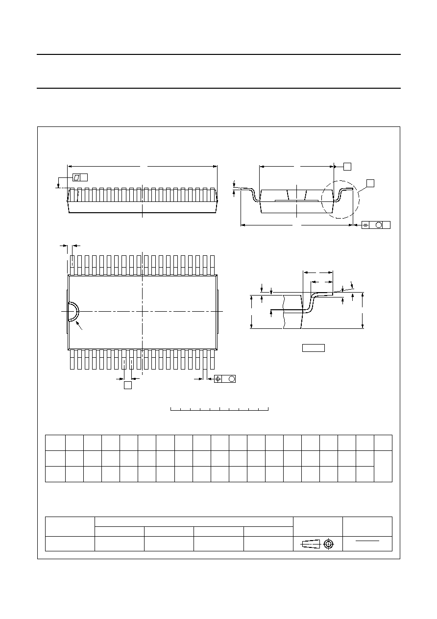
PACKAGE OUTLINES
UNIT
A
1
A
2
A
3
b
p
c
D
(1)
E
(2)
Z
(1)
e
H
E
L
L
p
Q
y
w
v
REFERENCES
OUTLINE
VERSION
EUROPEAN
PROJECTION
ISSUE DATE
IEC
JEDEC
EIAJ
mm
inches
0.3
0.1
2.45
2.25
0.25
0.42
0.30
0.22
0.14
15.6
15.2
7.6
7.5
0.762
2.25
12.3
11.8
1.15
1.05
0.6
0.3
7
0
o
o
0.1
0.1
DIMENSIONS (inch dimensions are derived from the original mm dimensions)
Notes
1. Plastic or metal protrusions of 0.4 mm maximum per side are not included.
2. Plastic interlead protrusions of 0.25 mm maximum per side are not included.
1.7
1.5
SOT158-1
92-11-17
95-01-24
X
w
M
A
A
1
A
2
b
p
D
H
E
L
p
Q
detail X
E
Z
e
c
L
v
M
A
(A )
3
A
y
40
20
21
1
pin 1 index
0.012
0.004
0.096
0.089
0.017
0.012
0.0087
0.0055
0.61
0.60
0.30
0.29
0.03
0.089
0.48
0.46
0.045
0.041
0.024
0.012
0.004
0.2
0.008
0.004
0.067
0.059
0.010
0
5
10 mm
scale
VSO40: plastic very small outline package; 40 leads
SOT158-1
A
max.
2.70
0.11
1996 Jun 18
19
Philips Semiconductors
Product specification
Front-end and PLL synthesizers for
car radios
TEA6810V; TEA6811V
UNIT
A
1
A
2
A
3
b
p
c
D
(1)
E
(2)
e
H
E
L
L
p
Q
y
w
v
REFERENCES
OUTLINE
VERSION
EUROPEAN
PROJECTION
ISSUE DATE
IEC
JEDEC
EIAJ
mm
inches
0.3
0.1
2.45
2.25
0.25
0.42
0.30
0.22
0.14
15.6
15.2
7.6
7.5
0.762
12.3
11.8
1.15
1.05
0.6
0.3
7
0
o
o
0.1
0.1
DIMENSIONS (inch dimensions are derived from the original mm dimensions)
Note
1. Plastic or metal protrusions of 0.4 mm maximum per side are not included.
2. Plastic interlead protrusions of 0.25 mm maximum per side are not included.
1.7
1.5
SOT158-2
X
w
M
A
A
1
A
2
b
p
D
H
E
L
p
Q
detail X
E
Z
e
c
L
v
M
A
(A )
3
A
y
40
21
20
1
pin 1 index
0.012
0.004
0.096
0.089
0.017
0.012
0.0087
0.0055
0.61
0.60
0.30
0.29
0.03
2.25
0.089
0.48
0.46
0.045
0.041
0.024
0.012
0.004
0.2
0.008
0.004
0.067
0.059
0.010
Z
(1)
0
5
10 mm
scale
92-11-17
95-01-24
VSO40: plastic very small outline package; 40 leads; face down
SOT158-2
A
max.
2.70
0.11

1996 Jun 18
20
Philips Semiconductors
Product specification
Front-end and PLL synthesizers for
car radios
TEA6810V; TEA6811V
SOLDERING
Introduction
There is no soldering method that is ideal for all IC
packages. Wave soldering is often preferred when
through-hole and surface mounted components are mixed
on one printed-circuit board. However, wave soldering is
not always suitable for surface mounted ICs, or for
printed-circuits with high population densities. In these
situations reflow soldering is often used.
This text gives a very brief insight to a complex technology.
A more in-depth account of soldering ICs can be found in
our
"IC Package Databook" (order code 9398 652 90011).
Reflow soldering
Reflow soldering techniques are suitable for all VSO
packages.
Reflow soldering requires solder paste (a suspension of
fine solder particles, flux and binding agent) to be applied
to the printed-circuit board by screen printing, stencilling or
pressure-syringe dispensing before package placement.
Several techniques exist for reflowing; for example,
thermal conduction by heated belt. Dwell times vary
between 50 and 300 seconds depending on heating
method. Typical reflow temperatures range from
215 to 250
∞
C.
Preheating is necessary to dry the paste and evaporate
the binding agent. Preheating duration: 45 minutes at
45
∞
C.
Wave soldering
Wave soldering techniques can be used for all VSO
packages if the following conditions are observed:
∑
A double-wave (a turbulent wave with high upward
pressure followed by a smooth laminar wave) soldering
technique should be used.
∑
The longitudinal axis of the package footprint must be
parallel to the solder flow.
∑
The package footprint must incorporate solder thieves at
the downstream end.
During placement and before soldering, the package must
be fixed with a droplet of adhesive. The adhesive can be
applied by screen printing, pin transfer or syringe
dispensing. The package can be soldered after the
adhesive is cured.
Maximum permissible solder temperature is 260
∞
C, and
maximum duration of package immersion in solder is
10 seconds, if cooled to less than 150
∞
C within
6 seconds. Typical dwell time is 4 seconds at 250
∞
C.
A mildly-activated flux will eliminate the need for removal
of corrosive residues in most applications.
Repairing soldered joints
Fix the component by first soldering two diagonally-
opposite end leads. Use only a low voltage soldering iron
(less than 24 V) applied to the flat part of the lead. Contact
time must be limited to 10 seconds at up to 300
∞
C. When
using a dedicated tool, all other leads can be soldered in
one operation within 2 to 5 seconds between
270 and 320
∞
C.
1996 Jun 18
21
Philips Semiconductors
Product specification
Front-end and PLL synthesizers for
car radios
TEA6810V; TEA6811V
DEFINITIONS
LIFE SUPPORT APPLICATIONS
These products are not designed for use in life support appliances, devices, or systems where malfunction of these
products can reasonably be expected to result in personal injury. Philips customers using or selling these products for
use in such applications do so at their own risk and agree to fully indemnify Philips for any damages resulting from such
improper use or sale.
PURCHASE OF PHILIPS I
2
C COMPONENTS
Data sheet status
Objective specification
This data sheet contains target or goal specifications for product development.
Preliminary specification
This data sheet contains preliminary data; supplementary data may be published later.
Product specification
This data sheet contains final product specifications.
Limiting values
Limiting values given are in accordance with the Absolute Maximum Rating System (IEC 134). Stress above one or
more of the limiting values may cause permanent damage to the device. These are stress ratings only and operation
of the device at these or at any other conditions above those given in the Characteristics sections of the specification
is not implied. Exposure to limiting values for extended periods may affect device reliability.
Application information
Where application information is given, it is advisory and does not form part of the specification.
Purchase of Philips I
2
C components conveys a license under the Philips' I
2
C patent to use the
components in the I
2
C system provided the system conforms to the I
2
C specification defined by
Philips. This specification can be ordered using the code 9398 393 40011.

1996 Jun 18
22
Philips Semiconductors
Product specification
Front-end and PLL synthesizers for
car radios
TEA6810V; TEA6811V
NOTES

1996 Jun 18
23
Philips Semiconductors
Product specification
Front-end and PLL synthesizers for
car radios
TEA6810V; TEA6811V
NOTES

Internet: http://www.semiconductors.philips.com/ps/
(1)
ADDRESS CONTENT SOURCE April 6, 1998
Philips Semiconductors ≠ a worldwide company
© Philips Electronics N.V. 1996
SCA49
All rights are reserved. Reproduction in whole or in part is prohibited without the prior written consent of the copyright owner.
The information presented in this document does not form part of any quotation or contract, is believed to be accurate and reliable and may be changed
without notice. No liability will be accepted by the publisher for any consequence of its use. Publication thereof does not convey nor imply any license
under patent- or other industrial or intellectual property rights.
Netherlands: Postbus 90050, 5600 PB EINDHOVEN, Bldg. VB,
Tel. +31 40 27 83749, Fax. +31 40 27 88399
New Zealand: 2 Wagener Place, C.P.O. Box 1041, AUCKLAND,
Tel. +64 9 849 4160, Fax. +64 9 849 7811
Norway: Box 1, Manglerud 0612, OSLO,
Tel. +47 22 74 8000, Fax. +47 22 74 8341
Philippines: Philips Semiconductors Philippines Inc.,
106 Valero St. Salcedo Village, P.O. Box 2108 MCC, MAKATI,
Metro MANILA, Tel. +63 2 816 6380, Fax. +63 2 817 3474
Poland: Ul. Lukiska 10, PL 04-123 WARSZAWA,
Tel. +48 22 612 2831, Fax. +48 22 612 2327
Portugal: see Spain
Romania: see Italy
Russia: Philips Russia, Ul. Usatcheva 35A, 119048 MOSCOW,
Tel. +7 095 926 5361, Fax. +7 095 564 8323
Singapore: Lorong 1, Toa Payoh, SINGAPORE 1231,
Tel. +65 350 2538, Fax. +65 251 6500
Slovakia: see Austria
Slovenia: see Italy
South Africa: S.A. PHILIPS Pty Ltd., 195-215 Main Road Martindale,
2092 JOHANNESBURG, P.O. Box 7430 Johannesburg 2000,
Tel. +27 11 470 5911, Fax. +27 11 470 5494
South America: Rua do Rocio 220 - 5th floor, Suite 51,
CEP: 04552-903-S√O PAULO-SP, Brazil, P.O. Box 7383 (01064-970),
Tel. +55 11 821 2333, Fax. +55 11 829 1849
Spain: Balmes 22, 08007 BARCELONA,
Tel. +34 3 301 6312, Fax. +34 3 301 4107
Sweden: Kottbygatan 7, Akalla, S-16485 STOCKHOLM,
Tel. +46 8 632 2000, Fax. +46 8 632 2745
Switzerland: Allmendstrasse 140, CH-8027 ZÐRICH,
Tel. +41 1 488 2686, Fax. +41 1 481 7730
Taiwan: PHILIPS TAIWAN Ltd., 23-30F, 66,
Chung Hsiao West Road, Sec. 1, P.O. Box 22978,
TAIPEI 100, Tel. +886 2 382 4443, Fax. +886 2 382 4444
Thailand: PHILIPS ELECTRONICS (THAILAND) Ltd.,
209/2 Sanpavuth-Bangna Road Prakanong, BANGKOK 10260,
Tel. +66 2 745 4090, Fax. +66 2 398 0793
Turkey: Talatpasa Cad. No. 5, 80640 GÐLTEPE/ISTANBUL,
Tel. +90 212 279 2770, Fax. +90 212 282 6707
Ukraine: PHILIPS UKRAINE, 2A Akademika Koroleva str., Office 165,
252148 KIEV, Tel. +380 44 476 0297/1642, Fax. +380 44 476 6991
United Kingdom: Philips Semiconductors Ltd., 276 Bath Road, Hayes,
MIDDLESEX UB3 5BX, Tel. +44 181 730 5000, Fax. +44 181 754 8421
United States: 811 East Arques Avenue, SUNNYVALE, CA 94088-3409,
Tel. +1 800 234 7381, Fax. +1 708 296 8556
Uruguay: see South America
Vietnam: see Singapore
Yugoslavia: PHILIPS, Trg N. Pasica 5/v, 11000 BEOGRAD,
Tel. +381 11 825 344, Fax.+381 11 635 777
For all other countries apply to: Philips Semiconductors, Marketing & Sales Communications,
Building BE-p, P.O. Box 218, 5600 MD EINDHOVEN, The Netherlands, Fax. +31 40 27 24825
Argentina: see South America
Australia: 34 Waterloo Road, NORTH RYDE, NSW 2113,
Tel. +61 2 805 4455, Fax. +61 2 805 4466
Austria: Computerstr. 6, A-1101 WIEN, P.O. Box 213,
Tel. +43 1 60 101, Fax. +43 1 60 101 1210
Belarus: Hotel Minsk Business Center, Bld. 3, r. 1211, Volodarski Str. 6,
220050 MINSK, Tel. +375 172 200 733, Fax. +375 172 200 773
Belgium: see The Netherlands
Brazil: see South America
Bulgaria: Philips Bulgaria Ltd., Energoproject, 15th floor,
51 James Bourchier Blvd., 1407 SOFIA,
Tel. +359 2 689 211, Fax. +359 2 689 102
Canada: PHILIPS SEMICONDUCTORS/COMPONENTS,
Tel. +1 800 234 7381, Fax. +1 708 296 8556
China/Hong Kong: 501 Hong Kong Industrial Technology Centre,
72 Tat Chee Avenue, Kowloon Tong, HONG KONG,
Tel. +852 2319 7888, Fax. +852 2319 7700
Colombia: see South America
Czech Republic: see Austria
Denmark: Prags Boulevard 80, PB 1919, DK-2300 COPENHAGEN S,
Tel. +45 32 88 2636, Fax. +45 31 57 1949
Finland: Sinikalliontie 3, FIN-02630 ESPOO,
Tel. +358 615 800, Fax. +358 615 80920
France: 4 Rue du Port-aux-Vins, BP317, 92156 SURESNES Cedex,
Tel. +33 1 40 99 6161, Fax. +33 1 40 99 6427
Germany: Hammerbrookstraþe 69, D-20097 HAMBURG,
Tel. +49 40 23 52 60, Fax. +49 40 23 536 300
Greece: No. 15, 25th March Street, GR 17778 TAVROS,
Tel. +30 1 4894 339/911, Fax. +30 1 4814 240
Hungary: see Austria
India: Philips INDIA Ltd, Shivsagar Estate, A Block, Dr. Annie Besant Rd.
Worli, MUMBAI 400 018, Tel. +91 22 4938 541, Fax. +91 22 4938 722
Indonesia: see Singapore
Ireland: Newstead, Clonskeagh, DUBLIN 14,
Tel. +353 1 7640 000, Fax. +353 1 7640 200
Israel: RAPAC Electronics, 7 Kehilat Saloniki St, TEL AVIV 61180,
Tel. +972 3 645 0444, Fax. +972 3 648 1007
Italy: PHILIPS SEMICONDUCTORS, Piazza IV Novembre 3,
20124 MILANO, Tel. +39 2 6752 2531, Fax. +39 2 6752 2557
Japan: Philips Bldg 13-37, Kohnan 2-chome, Minato-ku, TOKYO 108,
Tel. +81 3 3740 5130, Fax. +81 3 3740 5077
Korea: Philips House, 260-199 Itaewon-dong, Yongsan-ku, SEOUL,
Tel. +82 2 709 1412, Fax. +82 2 709 1415
Malaysia: No. 76 Jalan Universiti, 46200 PETALING JAYA, SELANGOR,
Tel. +60 3 750 5214, Fax. +60 3 757 4880
Mexico: 5900 Gateway East, Suite 200, EL PASO, TEXAS 79905,
Tel. +1 800 234 7381, Fax. +1 708 296 8556
Middle East: see Italy
Printed in The Netherlands
517021/02/pp24
Date of release: 1996 Jun 18
Document order number:
9397 750 00916