
DATA SHEET
Product specification
Supersedes data of 2004 Jan 08
2004 Oct 21
INTEGRATED CIRCUITS
TEA6848H
New In Car Entertainment car radio
tuner IC with Precision Adjacent
Channel Suppression
(NICE-PACS)

2004 Oct 21
2
Philips Semiconductors
Product specification
New In Car Entertainment car radio tuner IC with
Precision Adjacent Channel Suppression (NICE-PACS)
TEA6848H
CONTENTS
1
FEATURES
2
GENERAL DESCRIPTION
3
ORDERING INFORMATION
4
QUICK REFERENCE DATA
5
BLOCK DIAGRAM
6
PINNING
7
FUNCTIONAL DESCRIPTION
7.1
Oscillators
7.1.1
VCO
7.1.2
PLL
7.1.3
Crystal oscillator
7.2
DAA
7.3
FM signal channel
7.3.1
FM mixer 1
7.3.2
Buffer output for weather band flag
(pin WBFLAG)
7.3.3
FM keyed AGC
7.3.4
FM IF amplifier
7.3.5
FM mixer 2
7.3.6
FM IF2 dynamic selectivity
7.3.7
FM quadrature demodulator
7.3.8
Adjacent channel detector and threshold
extension
7.3.9
Bandwidth control `active' flag (pin IFBWFLAG)
7.3.10
Bandwidth control monitor voltage (pin V
IFBW
)
7.4
AM signal channel
7.4.1
AM tuner including mixer 1 and mixer 2
7.4.2
AM RF AGC
7.4.3
AM detector
7.4.4
AM noise blanker
7.5
FM and AM level detector
7.6
IF2 filter gain alignment
7.7
Frequency offset detector/alignment
8
LIMITING VALUES
9
THERMAL CHARACTERISTICS
10
DC CHARACTERISTICS
11
AC CHARACTERISTICS
12
I
2
C-BUS PROTOCOL
12.1
I
2
C-bus specification
12.1.1
Data transfer
12.1.2
I
2
C-bus pull-up resistors
12.1.3
Frequency setting
12.1.4
Default settings
12.1.5
Timing requirements
12.2
I
2
C-bus protocol
12.2.1
Data transfer mode and IC address
12.2.2
Write mode: data byte 0
12.2.3
Write mode: data byte 1
12.2.4
Write mode: data byte 2
12.2.5
Write mode: data byte 3
12.2.6
Write mode: data byte 4
12.2.7
Write mode: data byte 5
12.2.8
Write mode: data byte 6
12.2.9
Write mode: data byte 7
12.2.10
Read mode: data byte 0
13
TEST AND APPLICATION INFORMATION
14
INTERNAL CIRCUITRY
15
PACKAGE OUTLINE
16
SOLDERING
16.1
Introduction to soldering surface mount
packages
16.2
Reflow soldering
16.3
Wave soldering
16.4
Manual soldering
16.5
Suitability of surface mount IC packages for
wave and reflow soldering methods
17
DATA SHEET STATUS
18
DEFINITIONS
19
DISCLAIMERS
20
PURCHASE OF PHILIPS I
2
C COMPONENTS

2004 Oct 21
3
Philips Semiconductors
Product specification
New In Car Entertainment car radio tuner IC with
Precision Adjacent Channel Suppression (NICE-PACS)
TEA6848H
1
FEATURES
∑
FM mixer 1 for conversion of FM RF (65 to 108 MHz
and US weather band) to IF of 10.7 MHz; the mixer
provides inherent image rejection; for European and
US FM band/WB (weather band) the mixer is driven with
a `high' injection Local Oscillator (LO); in Japan
FM band and East Europe FM band the mixer is driven
with a `low' injection LO
∑
AM mixer 1 for conversion of AM RF to AM IF1 of
10.7 MHz
∑
LC tuner oscillator providing mixer frequencies for
FM mixer and AM mixer 1
∑
AM mixer 2 for conversion of AM IF1 to AM IF2 of
450 kHz
∑
Crystal oscillator providing mixer frequencies for
AM mixer 2 and FM mixer 2 and reference for
synthesizer PLL, IF count, timing for Radio Data System
(RDS) update and reference frequency for car audio
signal processor ICs
∑
Fast synthesizer PLL tuning system with local control for
inaudible RDS updating
∑
Timing function for RDS update algorithm and control
signal output for car audio signal processor ICs
(TEA688x, SAA77xx, TEF689x)
∑
Digital alignment circuit for bus controlled matching of
oscillator tuning voltage to FM antenna tank circuit
tuning voltage
∑
AGC PIN diode drive circuit for FM RF AGC; AGC
detection at FM mixer input; the AGC PIN diode drive
can be activated by the I
2
C-bus as a local function for
search tuning; AGC threshold is a programmable and
keyed function switchable via the I
2
C-bus
∑
FM IF linear amplifier with high dynamic input range
∑
FM mixer 2 for conversion of FM IF1 to FM IF2 of
450 kHz with inherent image rejection
∑
Fully integrated dynamic selectivity and
FM demodulator at IF2; improved sensitivity with
dynamic threshold extension; centre frequency of IF2
selectivity alignment via the I
2
C-bus
∑
Level detector for AM and FM with temperature
compensated output voltage; starting point and slope of
level output is programmable via the I
2
C-bus
∑
AM cascode AGC stage and RF PIN diode drive circuit;
AGC threshold detection at AM mixer 1 and IF2 AGC
input; threshold for detection at mixer 1 input is
programmable via the I
2
C-bus
∑
AM IF2 AGC and demodulator
∑
AM AF output switchable to provide AM IF2 for
AM stereo decoder
∑
AM noise blanker with detection at IF1 and blanking at
AM IF2
∑
Software controlled flag output
∑
Buffer output for weather band flag
∑
Adjacent channel detector, modulation detector and
frequency offset for instantaneous bandwidth control of
the integrated filter
∑
Flag and voltage output indicating the actual bandwidth
∑
I
2
C-bus alignment of centre frequency and gain variation
as functions of bandwidth of the IF2 filter and centre
frequency of the offset detector.
2
GENERAL DESCRIPTION
The TEA6848H is a single IC with car radio tuner for AM,
FM and Weather Band (WB) intended for microcontroller
tuning with the I
2
C-bus. It provides the following functions:
∑
AM double conversion receiver for LW, MW and SW
(31 m, 41 m and 49 m bands) with IF1 = 10.7 MHz and
IF2 = 450 kHz
∑
FM double conversion receiver with integrated image
rejection for IF1 and for IF2 capable of selecting US FM,
US weather, Europe FM, East Europe FM and
Japan FM bands; fully integrated dynamic selectivity at
450 kHz FM IF2; FM demodulator with dynamic
threshold extension; centre frequency alignment of IF2
selectivity via the I
2
C-bus
∑
The tuning system includes VCO, crystal oscillator and
PLL synthesizer on one chip.
3
ORDERING INFORMATION
TYPE NUMBER
PACKAGE
NAME
DESCRIPTION
VERSION
TEA6848H
LQFP80
plastic low profile quad flat package; 80 leads; body 12
◊
12
◊
1.4 mm
SOT315-1

2004 Oct 21
4
Philips Semiconductors
Product specification
New In Car Entertainment car radio tuner IC with
Precision Adjacent Channel Suppression (NICE-PACS)
TEA6848H
4
QUICK REFERENCE DATA
SYMBOL
PARAMETER
CONDITIONS
MIN.
TYP.
MAX.
UNIT
V
DDA(n)
analog supply voltage 1 to 4 and 6
8
8.5
9
V
I
DDA(tot)
sum of analog supply
currents 1 to 4 and 6
FM mode
45
56
67
mA
AM mode
40
50
60
mA
V
DDA5
analog supply voltage 5
4.75
5
5.25
V
I
DDA5
analog supply current 5
FM mode
-
7.4
-
mA
AM mode
-
11
-
mA
V
DDD
digital supply voltage
4.75
5
5.25
V
I
DDD
digital supply current
FM mode
21
26
31
mA
AM mode
22
27
32
mA
f
AM(ant)
AM input frequency
LW
0.144
-
0.288
MHz
MW
0.522
-
1.710
MHz
SW
5.730
-
9.99
MHz
f
FM(ant)
FM input frequency
65
-
108
MHz
f
FM(WB)(ant)
FM weather band input frequency
162.4
-
162.55
MHz
T
amb
ambient temperature
-
40
-
+85
∞
C
AM overall system parameters; see Figs 10 and 11
(S+N)/N
signal plus noise-to-noise ratio
m = 0.3; B
AF
= 2.15 kHz
-
59
-
dB
THD
total harmonic distortion
m = 0.8; f
mod
= 1 kHz
-
0.3
-
%
V
sens(rms)
sensitivity (RMS value)
m = 0.3; f
mod
= 1 kHz;
(S+N)/N = 26 dB;
with European dummy
aerial 15 pF/60 pF;
B
AF
= 2.15 kHz
-
45
-
µ
V
FM overall system parameters; see Figs 10 and 11
(S+N)/N
signal plus noise-to-noise ratio
f = 22.5 kHz;
de-emphasis = 50
µ
s;
B
AF
= 300 Hz to 15 kHz
-
63
-
dB
THD
total harmonic distortion
f = 75 kHz;
with 2
◊
SFE10.7MS3
-
0.35
-
%
V
sens(rms)
sensitivity (RMS value)
f = 22.5 kHz;
f
mod
= 1 kHz;
(S+N)/N = 26 dB;
de-emphasis = 50
µ
s;
B
AF
= 300 Hz to 15 kHz;
with 75
dummy antenna
-
1.4
2
µ
V
2004 Oct 21
5
Philips Semiconductors
Product specification
Ne
w In Car Enter
tainment car r
adio tuner IC with
Precision
Adjacent
Channel
Suppression
(NICE-P
A
CS)
TEA6848H
This text is here in white to force landscape pages to be rotated correctly when browsing through the pdf in the Acrobat reader.This text is here in
_
white to force landscape pages to be rotated correctly when browsing through the pdf in the Acrobat reader.This text is here inThis text is here in
white to force landscape pages to be rotated correctly when browsing through the pdf in the Acrobat reader. white to force landscape pages to be ...
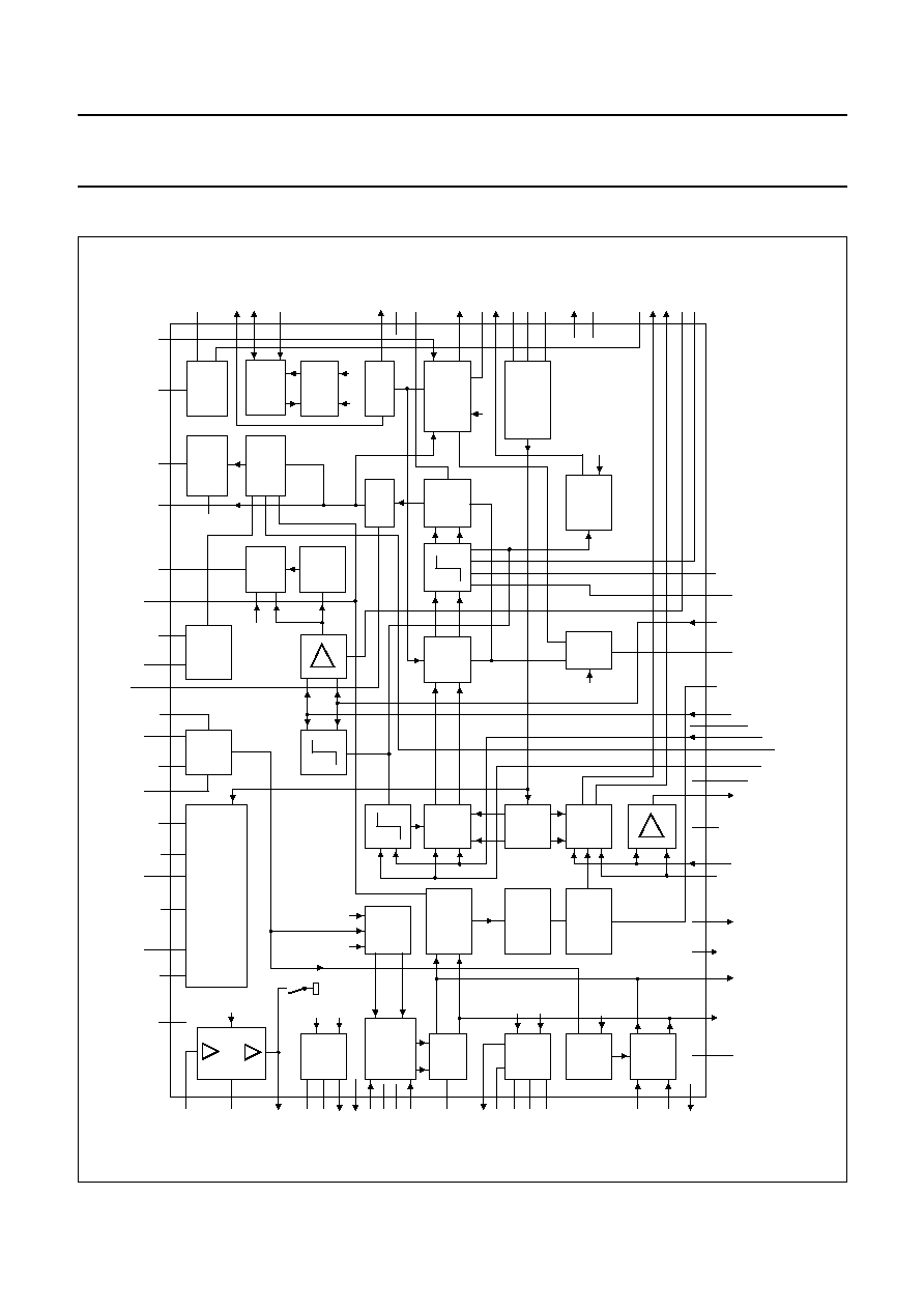
5
BLOCK DIA
GRAM
handbook, full pagewidth
DAA
RDS
UPDATE
CRYSTAL
OSCILLATOR
POWER
SUPPLY
VCO
AM
MIXER 1
AM
MIXER 2
AM
AGC
90
∞
FM
I/Q MIXER 1
FM
AGC
TUNING SYSTEM
AM NOISE
DETECTOR
PEAK/
AVERAGE
BLANK
PULSE
LEVEL
DAA
˜
10/
˜
20
˜
1/
˜
2/
˜
3
90
∞
IF
COUNT
TEA6848H
AM
DEMOD
FM
MIXER 2
˜
2
MUX
IF
FILTER
FM
DEMOD
STABI
BUFFER
BANDWIDTH
CONTROL
x1/ x15
AMPLIFIER
MPXOUT
19
18
15
14
13
12 11 10 9 8 7 6
5
4
3
2
1
20
22
23
24
25
26
27
28
29
30
31
32
33
34
35
36
37
38
39
40
DAAIN
DAATD
DAAOUT
TKEYEDAGC
TFMAGC
IFMAGC
WBFLAG
FMMIXIN2
FMMIXIN1
Vref(MIX)
i.c.
RFGND
IAMAGC
VAMCAS
VAMCASFB
AMMIX1IN
AMMIX1DEC
SWFLAG
VDDA2
MIX1OUT2
MIX1OUT1
FMLIMDCFDB1
AMIF2DEC
AMNBHOLD
IFAMPOUT
IFCDAATEST
FMMIX2DEC
COFFSET
FMMIX2IN
IF1GND
AMIF2IN
VDDA1
IFAMPIN
IFAMPDEC
IF2FILQ
IF2FILI
FMLIMDCFDB2
IREFFMIF2
THFAMAGC
TAFAMAGC
41
42
43
44
45
46
47
48
49
50
52
51
53
54
55
56
57
58
59
60
MODDET
VDDA5
FMMPX
RDSMPX
AMAFIF2
TRDSMUTE
AFHOLD
AFSAMPLE
MPXDCFDB
VDDA4
OSCTNK
OSCFDB
VCOGND
DGND
VDDD
FREF
VDDA3
CPOUT
Vtune
i.c.
61
VDDA6
IFBWFLAG
SDA
SCL
VIFBW
IF2GND
CINT
MODETOUT
TACD
Vlevel(AMFM)
XTAL1
XTALGND
XTAL2
Vlevel(ACD)
ACDTHRES
IREF
AMMIX2OUT1
AMMIX2OUT2
CAGC
Vref(lim)
62
63
64
65
66
67
68
69
70
71
72
73
74
75
76
77
78
79
80
AM
LEVEL
LEVEL
WB
LEVEL
20.5 MHz
FM
AM
WB/JAPAN/OIRT
21
17
16
ANTENNA
AM STEREO
MUTE
RDS
I
2
C-bus
I
2
C-bus
I
2
C-bus
I
2
C-bus
I
2
C-bus
I
2
C-bus
I
2
C-BUS
I
2
C-
bus
MHC436
◊
◊
◊
◊
Fig.1 Block diagram.

2004 Oct 21
6
Philips Semiconductors
Product specification
New In Car Entertainment car radio tuner IC with
Precision Adjacent Channel Suppression (NICE-PACS)
TEA6848H
6
PINNING
SYMBOL
PIN
DESCRIPTION
FMLIMDCFDB1
1
decoupling in-phase FM limiter
FMLIMDCFDB2
2
decoupling quadrature phase FM limiter
AMIF2DEC
3
decoupling for AM IF2 input
IREFFMIF2
4
reference current for FM IF2
AMNBHOLD
5
AM noise blanker threshold
AMIF2IN
6
AM IF2 input (450 kHz) for demodulator AGC and AM level detector
IF1GND
7
AM IF1 ground
FMMIX2IN
8
FM mixer 2 input
COFFSET
9
DC feedback for offset compensation RDS mute
FMMIX2DEC
10
FM mixer 2 decoupling
IFCDAATEST
11
test pin for IF centre DAA
IFAMPOUT
12
IF amplifier output (10.7 MHz)
V
DDA1
13
analog supply voltage 1 (8.5 V) for FM IF amplifier
IFAMPIN
14
FM IF amplifier and AM mixer 2 input (10.7 MHz)
IFAMPDEC
15
FM IF amplifier and AM mixer 2 decoupling
IF2FILQ
16
test output quadrature phase FM IF2 filter
IF2FILI
17
test output in-phase FM IF2 filter
MIX1OUT1
18
FM mixer and AM mixer 1 IF output 1 (10.7 MHz)
MIX1OUT2
19
FM mixer and AM mixer 1 IF output 2 (10.7 MHz)
V
DDA2
20
analog supply voltage 2 (8.5 V) for FM and AM RF
SWFLAG
21
output software programmable flag
AMMIX1DEC
22
AM mixer 1 decoupling
AMMIX1IN
23
AM mixer 1 input
VAMCASFB
24
feedback for cascode AM AGC
VAMCAS
25
cascode AM AGC
TAFAMAGC
26
AF time constant of AM front-end AGC
THFAMAGC
27
HF time constant of AM front-end AGC
IAMAGC
28
PIN diode drive current output of AM front-end AGC
V
ref(MIX)
29
reference voltage for FM RF mixer
FMMIXIN1
30
FM RF mixer input 1
RFGND
31
RF ground
i.c.
32
internal connection
FMMIXIN2
33
FM RF mixer input 2
WBFLAG
34
buffered weather band flag output
IFMAGC
35
PIN diode drive current output of FM front-end AGC
TFMAGC
36
time constant of FM front-end AGC
TKEYEDAGC
37
time constant of keyed FM front-end AGC
DAAOUT
38
output of digital auto alignment circuit for antenna tank circuit
DAATD
39
temperature compensation diode for digital auto alignment circuit for antenna tank circuit
DAAIN
40
input of digital auto alignment circuit for antenna tank circuit

2004 Oct 21
7
Philips Semiconductors
Product specification
New In Car Entertainment car radio tuner IC with
Precision Adjacent Channel Suppression (NICE-PACS)
TEA6848H
i.c.
41
internal connection
V
tune
42
tuning voltage
CPOUT
43
charge pump output
V
DDA3
44
analog supply voltage 3 (8.5 V) for tuning PLL
FREF
45
reference frequency output for signal processor IC
V
DDD
46
digital supply voltage (5 V)
DGND
47
digital ground
VCOGND
48
VCO ground
OSCFDB
49
VCO feedback
OSCTNK
50
VCO tank circuit
V
DDA4
51
analog supply voltage 4 (8.5 V) for VCO
MPXDCFDB
52
DC feedback for FM MPX signal path
AFSAMPLE
53
AF sample flag output for car audio signal processor IC
AFHOLD
54
AF hold flag output for car audio signal processor IC
TRDSMUTE
55
time constant for RDS update mute
AMAFIF2
56
AM demodulator AF output or IF2 output for AM stereo (multiplexed by I
2
C-bus)
RDSMPX
57
MPX output for RDS decoder and signal processor (not muted)
FMMPX
58
FM demodulator MPX output
V
DDA5
59
analog supply voltage 5 (5 V) for on-chip power supply
MODDET
60
modulation detector input
V
DDA6
61
analog supply voltage 6 (8.5 V) for on-chip power supply
IFBWFLAG
62
FM IF2 bandwidth flag output
SDA
63
I
2
C-bus data line input and output
SCL
64
I
2
C-bus clock line input
V
IFBW
65
monitor voltage for FM IF2 bandwidth
IF2GND
66
AM IF2 ground
CINT
67
demodulator loop filter
MODETOUT
68
modulation detector output
TACD
69
adjacent channel detector time constant
V
level(AMFM)
70
level voltage output for AM and FM
XTAL1
71
crystal oscillator 1
XTALGND
72
crystal oscillator ground
XTAL2
73
crystal oscillator 2
V
level(ACD)
74
level voltage output for adjacent channel detector
ACDTHRES
75
adjacent channel detector threshold
IREF
76
reference current for power supply
AMMIX2OUT1
77
AM mixer 2 output 1 (450 kHz)
AMMIX2OUT2
78
AM mixer 2 output 2 (450 kHz)
CAGC
79
AM IF AGC capacitor/offset detector alignment (FM)
V
ref(lim)
80
limiter reference voltage
SYMBOL
PIN
DESCRIPTION

2004 Oct 21
8
Philips Semiconductors
Product specification
New In Car Entertainment car radio tuner IC with
Precision Adjacent Channel Suppression (NICE-PACS)
TEA6848H
handbook, full pagewidth
TEA6848H
MHC437
1
2
3
4
5
6
7
8
9
10
11
12
13
14
15
16
17
18
19
20
60
59
58
57
56
55
54
53
52
51
50
49
48
47
46
45
44
43
42
41
21
22
23
24
25
26
27
28
29
30
31
32
33
34
35
36
37
38
39
40
80
79
78
77
76
75
74
73
72
71
70
69
68
67
66
65
64
63
62
61
V
ref(lim)
CAGC
AMMIX2OUT2
AMMIX2OUT1
IREF
ACDTHRES
V
level(ACD)
XTAL2
XTALGND
XTAL1
V
level(AMFM)
TACD
MODETOUT
CINT
IF2GND
V
IFBW
SCL
SDA
IFBWFLAG
V
DDA6
SWFLAG
AMMIX1DEC
AMMIX1IN
VAMCASFB
VAMCAS
TAFAMAGC
THFAMAGC
IAMAGC
V
ref(MIX)
FMMIXIN1
RFGND
i.c.
FMMIXIN2
WBFLAG
IFMAGC
TFMAGC
TKEYEDAGC
DAAOUT
DAATD
DAAIN
FMLIMDCFDB1
FMLIMDCFDB2
AMIF2DEC
IREFFMIF2
AMNBHOLD
AMIF2IN
IF1GND
FMMIX2IN
COFFSET
FMMIX2DEC
IFCDAATEST
IFAMPOUT
VDDA1
IFAMPIN
IFAMPDEC
IF2FILQ
IF2FILI
MIX1OUT1
MIX1OUT2
VDDA2
MODDET
VDDA5
FMMPX
RDSMPX
AMAFIF2
TRDSMUTE
AFHOLD
AFSAMPLE
MPXDCFDB
VDDA4
OSCTNK
OSCFDB
VCOGND
DGND
VDDD
FREF
VDDA3
CPOUT
Vtune
i.c.
Fig.2 Pin configuration.

2004 Oct 21
9
Philips Semiconductors
Product specification
New In Car Entertainment car radio tuner IC with
Precision Adjacent Channel Suppression (NICE-PACS)
TEA6848H
7
FUNCTIONAL DESCRIPTION
7.1
Oscillators
7.1.1
VCO
The varactor tuned VCO provides the local oscillator signal
for both FM and AM mixer 1. It has a frequency range of
162.9 to 248.2 MHz.
7.1.2
PLL
Fast synthesizer PLL tuning system with local control for
inaudible RDS updating.
7.1.3
C
RYSTAL OSCILLATOR
The crystal oscillator provides a 20.5 MHz signal that is
used for:
∑
Reference frequency for frequency synthesizer PLL
∑
Local oscillator for AM mixer 2 and FM mixer 2
∑
Reference frequency for the IF counter
∑
Timing signal for the RDS update algorithm
∑
Reference frequency (75.368 kHz) for the TEA688x (car
audio signal processor - CASP) or TEF689x (car radio
integrated signal processor - CRISP).
7.2
DAA
To reduce the number of manual alignments in production
the following I
2
C-bus controlled Digital Auto Alignment
(DAA) functions are included:
∑
FM RF DAA
≠ 7-bit DAA circuitry for the conversion of the VCO
tuning voltage to a controlled alignment voltage for
the FM antenna tank circuit
∑
FM and AM level DAA
≠ Level DAA circuitry for alignment of slope (3-bit) and
starting point (5-bit) of the level curve
∑
IF2 centre DAA
≠ Centre frequency alignment (7-bit) of integrated
FM IF2 dynamic selectivity.
7.3
FM signal channel
7.3.1
FM
MIXER
1
FM quadrature mixer converts FM RF (65 to 108 MHz and
weather band) to IF of 10.7 MHz. The FM mixer provides
inherent image rejection and high RF sensitivity.
It is capable of tuning the US FM, US weather,
Europe FM, Japan FM and East Europe FM bands:
∑
US FM = 87.9 to 107.9 MHz
∑
US weather FM = 162.4 to 162.55 MHz
∑
Europe FM = 87.5 to 108 MHz
∑
Japan FM = 76 to 91 MHz
∑
East Europe FM = 65 to 74 MHz.
7.3.2
B
UFFER OUTPUT FOR WEATHER BAND FLAG
(
PIN
WBFLAG)
The buffer output on pin WBFLAG is HIGH for weather
band mode.
7.3.3
FM
KEYED
AGC
The AGC threshold is programmable and the keyed AGC
function is switchable via the I
2
C-bus. AGC detection
occurs at the input of the first FM mixer. If the keyed AGC
function is activated, the AGC is keyed only by the narrow
band level. The AGC PIN diode drive can be activated via
the I
2
C-bus as a local function for search tuning. The AGC
sources a constant 10 mA current into the FM PIN diode in
AM mode.
7.3.4
FM IF
AMPLIFIER
The FM IF amplifier provides 18 dB amplification with high
linearity over a wide dynamic range.
7.3.5
FM
MIXER
2
The FM mixer 2 converts 10.7 MHz FM IF1 to 450 kHz
FM IF2 in I and Q phase to achieve image rejection in the
demodulator.

2004 Oct 21
10
Philips Semiconductors
Product specification
New In Car Entertainment car radio tuner IC with
Precision Adjacent Channel Suppression (NICE-PACS)
TEA6848H
7.3.6
FM IF2
DYNAMIC SELECTIVITY
The IF bandwidth of the FM IF2 is automatically adjusted
depending on modulation and reception conditions. The
centre frequency of the selectivity is adjusted by a 7-bit
instruction via the I
2
C-bus. The dynamic selectivity mode
and three fixed bandwidths (60, 90 and 130 kHz) can be
selected via the I
2
C-bus. The IF2 bandwidth is set to
13 kHz in weather band mode.
7.3.7
FM
QUADRATURE DEMODULATOR
The FM quadrature demodulator is adjustment free.
7.3.8
A
DJACENT CHANNEL DETECTOR AND THRESHOLD
EXTENSION
In the event of breakthrough of a strong neighbouring
transmitter, the IF2 bandwidth is reduced dynamically.
At low RF input voltages and low modulation levels the IF2
bandwidth is reduced to achieve improved sensitivity by
demodulator threshold extension.
7.3.9
B
ANDWIDTH CONTROL
`
ACTIVE
'
FLAG
(
PIN
IFBWFLAG)
Flag output IBFW = 1 from pin IFBWFLAG indicates that
the IF2 bandwidth is reduced.
7.3.10
B
ANDWIDTH CONTROL MONITOR VOLTAGE
(
PIN
V
IFBW
)
The actual bandwidth is indicated by a voltage at pin V
IFBW
that is proportional, not linear, to the IF bandwidth.
7.4
AM signal channel
7.4.1
AM
TUNER INCLUDING MIXER
1
AND MIXER
2
The AM tuner is realized in a double conversion technique
and is capable of selecting LW, MW and SW bands.
AM mixer 1 converts AM RF to IF1 of 10.7 MHz, while
AM mixer 2 converts IF1 of 10.7 MHz to IF2 of 450 kHz:
∑
LW = 144 to 288 kHz
∑
MW = 530 to 1710 kHz (US AM band)
∑
SW = 5.73 to 9.99 MHz (including the 31 m, 41 m and
49 m bands).
7.4.2
AM RF AGC
The AM wideband AGC in front of the first AM mixer is
realized first by a cascaded NPN transistor, which controls
the transconductance of the RF amplifier JFET with 10 dB
of AGC range. Second, an AM PIN diode stage with
antenna type and frequency dependent AGC range is
available. The minimum JFET drain source voltage is
controlled by a DC feedback loop (pin VAMCASFB) in
order to limit the cascode AGC range to 10 dB. If the
cascode AGC is not required, a simple RF AGC loop is
possible by using only a PIN diode. In this event
pins VAMCASFB and VAMCAS have to be open-circuit.
In FM mode, the cascade switches off the JFET bias
current to reduce total power consumption. The PIN diode
is biased by 1 mA in FM mode.
The AGC detection points for AM AGC are at the first AM
mixer input (threshold programmable via the I
2
C-bus) and
the IF2 AGC input (fixed threshold).
7.4.3
AM
DETECTOR
The AM output provides either a detected AM AF or the
corresponding AM IF2 signal. The IF2 signal can be used
for AM stereo decoder processing. Soft mute function is
controlled by the I
2
C-bus in AM mono mode.
7.4.4
AM
NOISE BLANKER
The detection point for the AM noise blanker is the output
stage of AM mixer 1, while blanking is realized at the
output of the mixer 2.
Trigger sensitivity can be modified by adding an external
resistor at pin AMNBHOLD.
7.5
FM and AM level detector
FM and AM level detectors provide the temperature
compensated output voltage. The starting points and
slopes of the level detector outputs are programmable via
the I
2
C-bus.

2004 Oct 21
11
Philips Semiconductors
Product specification
New In Car Entertainment car radio tuner IC with
Precision Adjacent Channel Suppression (NICE-PACS)
TEA6848H
7.6
IF2 filter gain alignment
The 4-bit filter gain alignment reduces the change in
IF filter gain spread when the bandwidth is changed in
dynamic mode from 155 kHz (maximum) to 25 kHz
(minimum).
A frequency has to be chosen in the middle of
European/US FM band, Japan band or OIRT band (for
East Europe) and the IC has to be set into dynamic
bandwidth mode (IF2 bandwidth is 155 kHz).
Setting and clearing the FMBW bit continuously allows the
adjustment of the gain alignment to minimum change in
AM/FM DC level.
7.7
Frequency offset detector/alignment
A very strong undesired neighbouring signal causes offset
in the demodulator in case of weak desired input signal.
The frequency offset detector reduces the bandwidth of
the IF2 filter when the detected offset in the demodulator
is too large.
There are four bits available for frequency offset detector
alignment. Every band has to be aligned separately.
Tuning has to be set to middle of the band, input signal
unmodulated, bit IFBW = 1 (alignment voltage will be
given to pin IFBWFLAG). The DC voltage at
pin IFBWFLAG has to be aligned to the minimum value.
8
LIMITING VALUES
In accordance with the Absolute Maximum Rating System (IEC 60134).
Notes
1. To avoid damage and wrong operation it is necessary to keep all 8.5 V supply voltages at a higher level than any 5 V
supply voltage. This is also necessary during power-on and power-down sequences. Precautions have to be
provided in such a way that interference cannot pull down the 8.5 V supply below the 5 V supply.
2. Machine model (R = 0
, C = 200 pF).
3. Human body model (R = 1.5 k
, C = 100 pF).
9
THERMAL CHARACTERISTICS
SYMBOL
PARAMETER
CONDITIONS
MIN.
MAX.
UNIT
V
DDA1
analog supply voltage 1 for FM IF amplifier
-
0.3
+10
V
V
DDA2
analog supply voltage 2 for FM and AM RF
-
0.3
+10
V
V
DDA3
analog supply voltage 3 for tuning PLL
-
0.3
+10
V
V
DDA4
analog supply voltage 4 for voltage controlled
oscillator
-
0.3
+10
V
V
DDA5
analog supply voltage 5 for on-chip power supply
-
0.3
+6.5
V
V
DDA6
analog supply voltage 6 for on-chip power supply
-
0.3
+10
V
V
DDD
digital supply voltage
-
0.3
+6.5
V
V
DD8.5-DD5
difference between any 8.5 V supply voltage and
any 5 V supply voltage
note 1
-
0.3
-
V
T
stg
storage temperature
-
55
+150
∞
C
T
amb
ambient temperature
-
40
+85
∞
C
V
es
electrostatic handling voltage
note 2
-
200
+200
V
note 3
-
2000
+2000
V
SYMBOL
PARAMETER
CONDITIONS
VALUE
UNIT
R
th(j-a)
thermal resistance from junction to ambient
in free air
54
K/W
R
th(j-c)
thermal resistance from junction to case
9
K/W

2004 Oct 21
12
Philips Semiconductors
Product specification
New In Car Entertainment car radio tuner IC with
Precision Adjacent Channel Suppression (NICE-PACS)
TEA6848H
10 DC CHARACTERISTICS
V
DDA(n)
= 8.5 V; V
DDA5
= 5 V; V
DDD
= 5 V; T
amb
= 25
∞
C; tested in the circuit of Figs 10 and 11; unless otherwise
specified.
SYMBOL
PARAMETER
CONDITIONS
MIN.
TYP.
MAX.
UNIT
Supply voltage
V
DDA(n)
analog supply voltages 1 to 4 and 6
8
8.5
9
V
V
DDA5
analog supply voltage 5
4.75
5
5.25
V
V
DDD
digital supply voltage
4.75
5
5.25
V
Supply current in FM mode
I
DDD
digital supply current
Europe/US band
21
26
31
mA
Japan/East Europe band
26.5
33
39.5
mA
I
DDA1
analog supply current 1 for FM IF
amplifier
5.5
7.3
8.8
mA
I
DDA2
analog supply current 2 for FM RF
4.2
5.2
6.2
mA
I
DDA3
analog supply current 3 for tuning PLL
3.2
4
4.8
mA
I
DDA4
analog supply current 4 for VCO
5.2
6.5
7.8
mA
I
DDA5
analog supply current 5 for on-chip
power supply
Europe/US band
-
3.8
-
mA
Japan/East Europe band
-
7.4
-
mA
I
DDA6
analog supply current 6 for on-chip
power supply
21.5
27
32.5
mA
I
MIX1OUT1
bias current of FM mixer output 1
4.8
6
7.2
mA
I
MIX1OUT2
bias current of FM mixer output 2
4.8
6
7.2
mA
Supply current in AM mode
I
DDD
digital supply current
22
27
32
mA
I
DDA1
analog supply current 1 for
AM mixer 2
100
120
140
µ
A
I
DDA2
analog supply current 2 for RF
1.4
1.8
2.2
mA
I
DDA3
analog supply current 3 for tuning PLL
1.8
2.2
2.6
mA
I
DDA4
analog supply current 4 for VCO
5
6.5
8
mA
I
DDA5
analog supply current 5 for on-chip
power supply
-
11
-
mA
I
DDA6
analog supply current 6 for on-chip
power supply
14
17.5
21
mA
I
MIX1OUT1
bias current of AM mixer 1 output 1
4.8
6
7.2
mA
I
MIX1OUT2
bias current of AM mixer 1 output 2
4.8
6
7.2
mA
I
AMMIX2OUT1
bias current of AM mixer 2 output 1
3.6
4.5
5.4
mA
I
AMMIX2OUT2
bias current of AM mixer 2 output 2
3.6
4.5
5.4
mA
On-chip power supply reference current generator: pin IREF
V
o(ref)
output reference voltage
R
IREF
= 120 k
4
4.25
4.5
V
R
o
output resistance
R
IREF
= 120 k
-
10
-
k
I
o(max)
maximum output current
R
IREF
= 120 k
-
100
-
+100
nA

2004 Oct 21
13
Philips Semiconductors
Product specification
New In Car Entertainment car radio tuner IC with
Precision Adjacent Channel Suppression (NICE-PACS)
TEA6848H
11 AC CHARACTERISTICS
V
DDA(n)
= V
MIX1OUT1
= V
MIX1OUT2
= V
AMMIX2OUT1
= V
AMMIX2OUT2
= 8.5 V; V
DDD
= V
DDA5
= 5 V; T
amb
= 25
∞
C; tested in the
circuit of Figs 10 and 11; all AC values are given in RMS; unless otherwise specified.
SYMBOL
PARAMETER
CONDITIONS
MIN.
TYP.
MAX.
UNIT
Voltage controlled oscillator
f
osc
oscillator frequency
162.9
-
248.2
MHz
C/N
carrier-to-noise ratio
f
osc
= 200 MHz;
f = 10 kHz
-
97
-
RR
ripple rejection
f
ripple
= 100 Hz;
V
DDA4(ripple)
= 100 mV (RMS);
f
osc
= 200 MHz
92
99
-
dB
Crystal oscillator
f
xtal
crystal frequency
-
20.5
-
MHz
C/N
carrier-to-noise ratio
f
xtal
= 20.5 MHz;
f = 10 kHz
-
112
-
C
IRCUIT INPUTS
:
PINS
XTAL1, XTALGND
AND
XTAL2
V
o(osc)(rms)
oscillator output voltage
(RMS value)
note 1
80
100
160
mV
V
XTAL1
, V
XTAL2
DC bias voltage
1.7
2.1
2.5
V
R
i
real part of input
impedance
V
XTAL1
-
V
XTAL2
= 1 mV; note 1
-
250
-
-
C
i
input capacitance
note 1
8
10
12
pF
Synthesizer
P
ROGRAMMABLE DIVIDER
N
prog
programmable divider ratio
512
-
32767
N
step
programmable divider step
size
-
1
-
C
HARGE PUMP
:
PIN
CPOUT
I
sink(cp1)l
low charge pump 1 sink
current
0.4 V < V
CPOUT
< 7.6 V;
data byte 3: bit 0 = 0, bit 1 = 1,
bit 2 = 1 for FM weather band;
f
VCO
> f
ref
◊
divider ratio
-
300
-
µ
A
I
source(cp1)l
low charge pump 1 source
current
0.4 V < V
CPOUT
< 7.6 V;
data byte 3: bit 0 = 0, bit 1 = 1,
bit 2 = 1 for FM weather band;
f
VCO
< f
ref
◊
divider ratio
-
-
300
-
µ
A
I
sink(cp1)h
high charge pump 1 sink
current
0.4 V < V
CPOUT
< 7.6 V;
data byte 3: bit 0 = 1, bit 1 = 1,
bit 2 = 1; AM stereo mode;
VCO divider = 10 (LW and MW);
f
VCO
> f
ref
◊
divider ratio
-
1
-
mA
dBc
Hz
------------
f
osc
f
osc
------------
dBc
Hz
------------

2004 Oct 21
14
Philips Semiconductors
Product specification
New In Car Entertainment car radio tuner IC with
Precision Adjacent Channel Suppression (NICE-PACS)
TEA6848H
I
source(cp1)h
high charge pump 1 source
current
0.4 V < V
CPOUT
< 7.6 V;
data byte 3: bit 0 = 1, bit 1 = 1,
bit 2 = 1; AM stereo mode;
VCO divider = 10 (LW and MW);
f
VCO
< f
ref
◊
divider ratio
-
-
1
-
mA
I
sink(cp2)
charge pump 2 sink current 0.3 V < V
CPOUT
< 7.1 V;
data byte 3: bit 0 = 0, bit 1 = 0,
bit 2 = 0; FM standard mode;
f
VCO
> f
ref
◊
divider ratio
-
130
-
µ
A
I
source(cp2)
charge pump 2 source
current
0.3 V < V
CPOUT
< 7.1 V;
data byte 3: bit 0 = 0, bit 1 = 0,
bit 2 = 0; FM standard mode;
f
VCO
< f
ref
◊
divider ratio
-
-
130
-
µ
A
C
HARGE PUMP
:
PIN
V
tune
I
sink(cp3)
charge pump 3 sink current 0.4 V < V
tune
< 7.6 V;
data byte 3: bit 0 = 0, bit 1 = 0,
bit 2 = 0; FM standard mode;
f
VCO
> f
ref
◊
divider ratio
-
3
-
mA
I
source(cp3)
charge pump 3 source
current
0.4 V < V
tune
< 7.6 V;
data byte 3: bit 0 = 0, bit 1 = 0,
bit 2 = 0; FM standard mode;
f
VCO
< f
ref
◊
divider ratio
-
-
3
-
mA
Antenna Digital Auto Alignment (DAA)
DAA
INPUT
:
PIN
DAAIN
I
bias(cp)
charge pump buffer input
bias current
V
DAAIN
= 0.4 to 8 V
-
10
-
+10
nA
V
i(cp)
charge pump buffer input
voltage
0
-
8.5
V
DAA
OUTPUT
:
PIN
DAAOUT; note 2
V
o(AM)
DAA output voltage in
AM mode
I
DAAOUT
< 100
µ
A
-
-
0.3
V
V
o(FM)
DAA output voltage in
FM mode
minimum value;
data byte 2 = 10000000;
V
DAAIN
= 0.5 V; V
DAATD
= 0.45 V
-
-
0.5
V
maximum value;
data byte 2 = 11111111;
V
DAAIN
= 4.7 V; V
DAATD
= 0.45 V
8
-
8.5
V
V
DAAIN
= 4 V; V
DAATD
= 0.45 V
data byte 2 = 10000000
-
0.65
-
V
data byte 2 = 11000000
3.8
4
4.2
V
V
DAAIN
= 2 V; V
DAATD
= 0.45 V
data byte 2 = 11010101
2.3
2.6
2.9
V
data byte 2 = 10101010
1.2
1.4
1.6
V
SYMBOL
PARAMETER
CONDITIONS
MIN.
TYP.
MAX.
UNIT

2004 Oct 21
15
Philips Semiconductors
Product specification
New In Car Entertainment car radio tuner IC with
Precision Adjacent Channel Suppression (NICE-PACS)
TEA6848H
V
o(n)
DAA output noise voltage
data byte 2 = 11000000;
FM mode; V
DAAIN
= 4 V;
V
DAATD
= 0.45 V;
B = 300 Hz to 22 kHz
-
30
100
µ
V
V
o(T)
DAA output voltage
variation with temperature
T
amb
=
-
40 to +85
∞
C;
data byte 2 = 11000000
-
8
-
+8
mV
V
o(step)
DAA step accuracy
n = 0 to 127; FM mode;
V
DAAOUT
= 0.5 to 8 V;
V
DAAIN
= 2 V; V
DAATD
= 0.45 V
0.5V
LSB
V
LSB
1.5V
LSB
mV
V
o(sink)
DAA output variation
caused by sink current
V
DAAIN
= 4 V; I
L
= 50
µ
A
-
V
LSB
-
+V
LSB
V
o(source)
DAA output variation
caused by source current
V
DAAIN
= 4 V; I
L
=
-
50
µ
A
-
V
LSB
-
+V
LSB
t
st
DAA output settling time
V
DAAOUT
= 0.2 to 8.25 V;
C
L
= 270 pF
-
20
30
µ
s
RR
ripple rejection
data byte 2 = 10101011;
FM mode; V
DAAIN
= 4 V;
V
DAATD
= 0.45 V; f
ripple
= 100 Hz;
V
DDA3(ripple)
= 100 mV (RMS)
-
65
-
dB
C
L
DAA output load
capacitance
-
-
270
pF
DAA
TEMPERATURE COMPENSATION
:
PIN
DAATD
I
source
compensation diode
source current
V
DAATD
= 0.2 to 1.2 V
-
50
-
40
-
30
µ
A
TC
source
temperature coefficient of
compensation diode
source current
V
DAATD
= 0.2 to 1.2 V;
T
amb
=
-
40 to +85
∞
C
-
300
-
+300
IF counter (FM IF2 or AM IF2 counter)
N
IF
IF counter length for
AM and FM
-
8
-
bit
P
INS
FMMIX2IN
AND
FMMIX2DEC; note 3
V
sens(rms)
sensitivity voltage
(RMS value)
FM mode
-
30
100
µ
V
N
counter result (decimal)
period = 2 ms;
V
FMMIX2IN-FMMIX2DEC
= 100
µ
V
prescaler ratio = 10
-
90
-
prescaler ratio = 40
-
22
-
period = 20 ms;
V
FMMIX2IN-FMMIX2DEC
= 100
µ
V
prescaler ratio = 10
-
132
-
prescaler ratio = 40
-
225
-
SYMBOL
PARAMETER
CONDITIONS
MIN.
TYP.
MAX.
UNIT
V
DAAOUT
V
DDA3
-----------------------
10
6
≠
K
-----------

2004 Oct 21
16
Philips Semiconductors
Product specification
New In Car Entertainment car radio tuner IC with
Precision Adjacent Channel Suppression (NICE-PACS)
TEA6848H
P
INS
AMIF2IN
AND
AMIF2DEC; note 4
V
sens(rms)
sensitivity voltage
(RMS value)
AM mode; m = 0
-
30
70
µ
V
N
counter result (decimal)
period = 2 ms;
V
AMIF2IN-AMIF2DEC
= 200
µ
V
-
132
-
period = 20 ms;
V
AMIF2IN-AMIF2DEC
= 200
µ
V
-
40
-
Reference frequency for car signal processor IC TEA688x and TEF689x; note 5
R
EFERENCE FREQUENCY DIVIDER
N
ref
crystal oscillator divider
ratio
-
272
-
f
ref
reference frequency
f
xtal
= 20.5 MHz
-
75.368
-
kHz
V
OLTAGE GENERATOR
:
PIN
FREF
V
o(p-p)
AC output voltage
(peak-to-peak value)
not loaded
60
90
-
mV
V
O
DC output voltage
3.2
3.4
3.7
V
R
o
output resistance
-
-
50
k
R
L(min)
minimum load resistance
for first I
2
C-bus address
1
-
-
M
Weather band flag: pin WBFLAG
I
source(max)
maximum source current
-
-
5
-
mA
R
i(shunt)
internal shunt resistance to
ground
-
50
-
k
V
o(max)
maximum output voltage
for FM mode
measured with respect to
pin RFGND
0
-
0.2
V
V
o
output voltage for weather
band mode
measured with respect to
pin RFGND
4
-
5
V
AM signal channel
AM RF AGC
STAGE
(PIN
DIODE DRIVE
)
V
i(p)
RF input voltage for
wideband AGC start level
(peak value)
m = 0.3; data byte 4: bit 5 = 0,
bit 6 = 0
-
150
-
mV
m = 0.3; data byte 4: bit 5 = 1,
bit 6 = 0
-
275
-
mV
m = 0.3; data byte 4: bit 5 = 0,
bit 6 = 1
-
400
-
mV
m = 0.3; data byte 4: bit 5 = 1,
bit 6 = 1
-
525
-
mV
AM IF AGC
STAGE INPUT
:
PIN
AMIF2IN
V
i(p)
IF2 input voltage
(peak value)
AGC start level
0.20
0.27
0.35
V
SYMBOL
PARAMETER
CONDITIONS
MIN.
TYP.
MAX.
UNIT

2004 Oct 21
17
Philips Semiconductors
Product specification
New In Car Entertainment car radio tuner IC with
Precision Adjacent Channel Suppression (NICE-PACS)
TEA6848H
AM RF AGC
CURRENT GENERATOR OUTPUT
:
PIN
IAMAGC
I
sink(max)
maximum AGC sink
current
V
o
= 2.8 V
11
15
19
mA
I
sink
AGC sink current
FM mode
1
-
-
mA
R
o
output resistance
I
o
= 1
µ
A
0.5
-
-
M
C
o
AM AGC current generator
output capacitance
-
5
7
pF
RF
CASCODE
AGC
I
cas(off)
AM cascode off current
FM mode
-
-
100
nA
Pin VAMCASFB
V
cas(FB)
cascode feedback voltage
V
AMMIX1IN-AMMIX1DEC
above
threshold; minimum gain
-
0.26
-
V
I
cas(FB)
cascode feedback sense
current
0
-
1
µ
A
Pin VAMCAS
V
cas
cascode voltage
V
AMMIX1IN-AMMIX1DEC
below
threshold; maximum gain
-
5
-
V
I
cas
cascode transistor base
current capability
100
-
-
µ
A
AM
MIXER
1 (IF1 = 10.7 MH
Z
)
Mixer inputs: pins AMMIX1DEC and AMMIX1IN
R
i
input resistance
note 6
15
25
40
k
C
i
input capacitance
note 6
2.5
5
7.5
pF
V
I
DC input voltage
2.3
2.7
3.1
V
V
i(max)
maximum input voltage
1 dB compression point of
V
MIX1OUT1-MIX1OUT2
; m = 0
500
-
-
mV
Mixer outputs: pins MIX1OUT1 and MIX1OUT2
R
o
output resistance
note 7
100
-
-
k
C
o
output capacitance
note 7
-
4
7
pF
V
o(max)(p-p)
maximum output voltage
(peak-to-peak value)
12
15
-
V
I
bias
mixer bias current
AM mode
4.8
6
7.2
mA
Mixer
g
m(conv)
conversion
transconductance
2.0
2.55
3.2
SYMBOL
PARAMETER
CONDITIONS
MIN.
TYP.
MAX.
UNIT
I
MIX1OUT
V
MIX1IN
---------------------
mA
V
---------

2004 Oct 21
18
Philips Semiconductors
Product specification
New In Car Entertainment car radio tuner IC with
Precision Adjacent Channel Suppression (NICE-PACS)
TEA6848H
g
m(conv)(T)
conversion
transconductance variation
with temperature
-
-
9
◊
10
-
4
-
K
-
1
IP3
3rd-order intermodulation
R
L
= 2.6 k
(AC load between
output pins);
f = 300 kHz
135
138
-
dB
µ
V
IP2
2nd-order intermodulation
R
L
= 2.6 k
(AC load between
output pins)
-
170
-
dB
µ
V
V
i(n)(eq)
equivalent input noise
voltage
band limited noise;
R
gen
= 750
; R
L
= 2.6 k
(AC load between output pins)
-
5.8
8
F
noise figure of AM mixer 1
-
4.5
7.1
dB
AM
MIXER
2 (IF2 = 450 kHz)
Mixer inputs: pins IFAMPIN and IFAMPDEC
R
i
input resistance
note 8
-
330
-
C
i
input capacitance
note 8
-
5
7
pF
V
I
DC voltage
2.4
2.7
3
V
V
i(max)(p)
maximum input voltage
(peak value)
1 dB compression point of
V
AMMIX2OUT1-AMMIX2OUT2
1.1
1.4
-
V
Mixer outputs: pins AMMIX2OUT1 and AMMIX2OUT2
R
o
output resistance
note 9
50
-
-
k
C
o
output capacitance
note 9
-
4
7
pF
V
o(max)(p-p)
maximum output voltage
(peak-to-peak value)
V
DDA6
= 8.5 V
12
15
-
V
I
bias
mixer bias current
AM mode
3.6
4.5
5.4
mA
Mixer
g
m(conv)
conversion
transconductance
1.3
1.6
1.9
g
m(conv)(T)
conversion
transconductance variation
with temperature
-
-
9
◊
10
-
4
-
K
-
1
IP3
3rd-order intermodulation
R
L
= 1.5 k
(AC load between
output pins);
f = 300 kHz
134
137
-
dB
µ
V
IP2
2nd-order intermodulation
R
L
= 1.5 k
(AC load between
output pins)
-
170
-
dB
µ
V
V
i(n)(eq)
equivalent input noise
voltage
R
gen
= 330
; R
L
= 1.5 k
(AC load between output pins)
-
15
22
SYMBOL
PARAMETER
CONDITIONS
MIN.
TYP.
MAX.
UNIT
g
m(conv)
g
m(conv)
T
◊
---------------------------------
nV
Hz
------------
I
AMMIX2OUT
V
IFAMPIN
----------------------------
mA
V
---------
g
m(conv)
g
m(conv)
T
◊
---------------------------------
nV
Hz
------------

2004 Oct 21
19
Philips Semiconductors
Product specification
New In Car Entertainment car radio tuner IC with
Precision Adjacent Channel Suppression (NICE-PACS)
TEA6848H
F
noise figure of AM mixer 2
-
16
19.5
dB
I
L
mixer leakage current
FM mode
-
-
10
µ
A
AM IF2 AGC
STAGE
:
PINS
AMIF2IN
AND
AMIF2DEC; note 4
V
i
input voltage
audio attenuation
=
-
10 dB
data byte 4: bit 4 = 1; mute on
-
25
40
µ
V
data byte 4: bit 4 = 0; mute off
-
6
10
µ
V
V
AGC(start)
AGC start voltage
input carrier voltage
-
14
30
µ
V
V
AGC(stop)
AGC stop voltage
maximum input peak voltage
1
-
-
V
V
AGC(ctrl)
AGC control voltage
V
i
= 1 mV
4.1
4.3
4.7
V
AGC
AGC range
between start and stop of AGC
-
89
-
dB
R
i
input resistance
1.8
2
2.2
k
C
i
input capacitance
-
10
15
pF
AM
DETECTOR
V
sens(rms)
sensitivity voltage
(RMS value)
m = 0.3; f
mod
= 400 Hz;
B
AF
= 2.15 kHz; R
gen
= 2 k
;
note 4
(S+N)/N = 26 dB
-
45
65
µ
V
(S+N)/N = 46 dB
-
600
900
µ
V
(S+N)/N
maximum signal plus
noise-to-noise ratio
m = 0.3; f
mod
= 400 Hz;
B
AF
= 2.15 kHz; R
gen
= 2 k
-
60
-
dB
THD
total harmonic distortion
B
AF
= 2.15 kHz; C
AGC
= 10
µ
F;
V
AMIF2IN
= 100
µ
V to 250 mV
(RMS)
m = 0.8; f
mod
= 400 Hz
-
0.5
1
%
m = 0.8; f
mod
= 100 Hz
-
1.25
2.5
%
t
sw
FM to AM switching time
V
AMIF2IN
= 100
µ
V; C
AGC
= 10
µ
F
-
1000
1500
ms
t
st
AM AGC settling time
V
AMIF2IN
= 100
µ
V to 100 mV
-
400
600
ms
V
AMIF2IN
= 100 mV to 100
µ
V
-
600
900
ms
Output: pin AMAFIF2
V
o(rms)
AM IF2 output voltage
(RMS value)
AM stereo; m = 0; data byte 3:
bit 0 = 1, bit 1 = 1, bit 2 = 1
minimum at V
AMIF2IN
= 14
µ
V
1.5
3
4.5
mV
maximum at V
AMIF2IN
= 5 mV
130
180
230
mV
AM mono; m = 0.3; data byte 3:
bit 0 = 1, bit 1 = 0, bit 2 = 1;
f
mod
= 400 Hz;
V
AMIF2IN
= 100
µ
V to 500 mV
(RMS)
200
250
300
mV
R
o
output resistance
data byte 3: bit 0 = 1, bit 1 = 1,
bit 2 = 1; AM stereo
-
-
500
data byte 3: bit 0 = 1, bit 1 = 0,
bit 2 = 1; AM mono
-
-
500
SYMBOL
PARAMETER
CONDITIONS
MIN.
TYP.
MAX.
UNIT

2004 Oct 21
20
Philips Semiconductors
Product specification
New In Car Entertainment car radio tuner IC with
Precision Adjacent Channel Suppression (NICE-PACS)
TEA6848H
C
o
output capacitance
data byte 3: bit 0 = 1, bit 1 = 0,
bit 2 = 1
-
5
7
pF
Z
L
load impedance
data byte 3: bit 0 = 1, bit 1 = 0,
bit 2 = 1; AM mono
100
-
-
k
data byte 3: bit 0 = 1, bit 1 = 1,
bit 2 = 1; AM stereo
10
-
-
k
RR
ripple rejection
V
DDA5(ripple)
= 100 mV (RMS);
f
ripple
= 100 Hz
-
24
-
dB
V
DDA6(ripple)
= 100 mV (RMS);
f
ripple
= 100 Hz
-
26
-
dB
AM IF2
LEVEL DETECTOR OUTPUT
:
PIN
V
level(AMFM)
; see Fig.4
V
level(AMFM)
DC output voltage
V
AMIF2IN
= 10
µ
V to 1 V
0
-
7
V
V
AMIF2IN
< 1
µ
V; standard setting
of level DAA
0.1
0.5
0.9
V
V
AMIF2IN
= 1.4 mV; standard
setting of level DAA
1.6
2.2
2.8
V
V
level(AMFM)
step size for adjustment of
level starting point
V
AMIF2IN
= 0 V; standard setting
of level slope
30
40
50
mV
V
level(slope)
slope of level voltage
V
AMIF2IN
= 140
µ
V to 140 mV;
standard setting of level slope
650
800
950
V
step
step size for adjustment of
level slope
V
AMIF2IN
= 1.4 mV
45
60
75
B
level(AMFM)
bandwidth of level output
voltage
V
AMIF2IN
= 15 mV; standard
setting of level DAA
200
300
-
kHz
R
o
output resistance
-
-
500
RR
ripple rejection
V
DDA6(ripple)
= 100 mV (RMS);
f
ripple
= 100 Hz
-
36
-
dB
AM
NOISE BLANKER
;
TEST SIGNAL AND TEST CIRCUIT
; see Fig.5
Threshold: pin AMNBHOLD
V
O
DC output voltage
4.3
4.6
5.1
V
t
sup
suppression time
V
pulse
= 200 mV (peak);
V
level(AMFM)
< 1.8 V
6
7.5
10
µ
s
f
trigger
trigger sensitivity frequency V
pulse
= 200 mV (peak);
V
leve(AMFM)l
< 1.8 V
-
1000
-
Hz
V
pulse
= 200 mV (peak);
V
level(AMFM)
> 2.2 V
-
-
100
Hz
V
pulse
= 20 mV (peak);
V
level(AMFM)
< 1.8 V
-
-
100
Hz
Noise detector output: pin TRDSMUTE
I
sink(AGC)
AM noise blanker AGC sink
current
V
TRDSMUTE
= 3 V
35
50
65
µ
A
SYMBOL
PARAMETER
CONDITIONS
MIN.
TYP.
MAX.
UNIT
mV
20 dB
---------------
mV
20 dB
---------------
V
level
V
DDA6
----------------

2004 Oct 21
21
Philips Semiconductors
Product specification
New In Car Entertainment car radio tuner IC with
Precision Adjacent Channel Suppression (NICE-PACS)
TEA6848H
V
AGC
AM noise blanker AGC
voltage
AM mixer 1 input V
i
= 0 V
1.9
2.2
2.5
V
FM signal channel
FM RF AGC (FM
DISTANCE MODE
;
DATA BYTE
4:
BIT
3 = 0)
Inputs: pins FMMIXIN1 and FMMIXIN2; note 10
V
i(RF)(rms)
RF input voltage for start of
wideband AGC
(RMS value)
data byte 4: bit 5 = 1, bit 6 = 1
-
3
-
mV
data byte 4: bit 5 = 0, bit 6 = 1
-
6
-
mV
data byte 4: bit 5 = 1, bit 6 = 0
-
9
-
mV
data byte 4: bit 5 = 0, bit 6 = 0
-
12
-
mV
Pin TFMAGC
R
source
source resistance
4
5
6
k
V
O(ref)
DC output reference
voltage
data byte 4: bit 5 = 0, bit 6 = 0;
V
FMMIXIN1-FMMIXIN2
= 0 V
4.1
4.6
5.1
V
PIN diode drive output: pin IFMAGC
I
sink(AGC)(max)
maximum AGC sink
current
V
IFMAGC
= 2.5 V;
V
TFMAGC
= V
O(ref)
-
0.5 V;
data byte 4: bit 5 = 0, bit 6 = 0,
bit 7 = 0
8
11.5
15
mA
I
source(AGC)(max)
maximum AGC source
current
V
IFMAGC
= 2.5 V;
V
TFMAGC
= V
O(ref)
+ 0.5 V;
data byte 4: bit 5 = 0, bit 6 = 0,
bit 7 = 0
-
15
-
11.5
-
8
mA
I
source(AGC)
AGC source current
AM mode
-
15
-
11.5
-
8
mA
V
IFMAGC
= 2.5 V; data byte 4:
bit 3 = 1 (FM local)
-
0.65
-
0.5
-
0.35
mA
Level voltage output: pin V
level(AMFM)
V
th
threshold voltage for
narrow-band AGC
data byte 4: bit 5 = 0, bit 6 = 0,
bit 7 = 1; keyed AGC
500
950
1400
mV
FM RF
MIXER
Reference voltage: pin V
ref(MIX)
V
ref
reference voltage
FM mode
6.5
7.1
7.9
V
AM mode
2.7
3.1
3.4
V
Inputs: pins FMMIXIN1 and FMMIXIN2; note 10
V
i(RF)(max)
maximum RF input voltage
1 dB compression point of
FM mixer output voltage
(peak-to-peak value)
70
100
-
mV
V
i(n)(eq)
equivalent input noise
voltage
R
gen
= 200
; R
L
= 2.6 k
-
2.6
3.1
R
i
input resistance
1.4
2.8
4.2
k
C
i
input capacitance
-
5
7
pF
SYMBOL
PARAMETER
CONDITIONS
MIN.
TYP.
MAX.
UNIT
nV
Hz
------------

2004 Oct 21
22
Philips Semiconductors
Product specification
New In Car Entertainment car radio tuner IC with
Precision Adjacent Channel Suppression (NICE-PACS)
TEA6848H
Outputs: pins MIX1OUT1 and MIX1OUT2; note 7
R
o
output resistance
100
-
-
k
C
o
output capacitance
2
3.5
5
pF
I
bias
mixer bias current
FM mode
4.8
6
7.2
mA
V
o(max)(p-p)
maximum output voltage
(peak-to-peak value)
3
-
-
V
FM mixer
g
m(conv)
conversion
transconductance
8.5
12.5
18
g
m(conv)(T)
conversion
transconductance variation
with temperature
-
-
1
◊
10
-
3
-
K
-
1
F
noise figure
-
3
4.6
dB
R
gen(opt)
optimum generator
resistance
-
200
-
IP3
3rd-order intermodulation
113
116
-
dB
µ
V
IRR
image rejection ratio
f
RFwanted
= 87.5 MHz;
f
RFimage
= 108.9 MHz
25
30
-
dB
data byte 3 = X010X110;
f
RFwanted
= 162.475 MHz;
f
RFimage
= 183.875 MHz; weather
band mode; f
ref
= 25 kHz
22
30
-
dB
IF
AMPLIFIER
G
gain
R
L
= 330
; V
IFAMPIN
= 1 mV;
note 8
15
17
19
dB
F
noise figure
-
10
13
dB
IP3
3rd-order intermodulation
113
116
-
dB
µ
V
Inputs: pins IFAMPIN and IFAMPDEC; note 8
V
i(max)(p)
maximum input voltage
(peak value)
1 dB compression point of
IF amplifier output voltage
(peak value)
200
-
-
mV
V
i(n)(eq)
equivalent input noise
voltage
R
gen
= 330
; R
L
= 330
-
8
10
R
i
input resistance
270
330
390
C
i
input capacitance
-
5
7
pF
Output: pin IFAMPOUT
V
o(max)(p)
maximum output voltage
(peak value)
1.2
1.5
-
V
R
o
output resistance
270
330
390
C
o
output capacitance
-
5
7
pF
SYMBOL
PARAMETER
CONDITIONS
MIN.
TYP.
MAX.
UNIT
mA
V
---------
V
MIX1OUTwanted
V
MIX1OUTimage
--------------------------------------
nV
Hz
------------

2004 Oct 21
23
Philips Semiconductors
Product specification
New In Car Entertainment car radio tuner IC with
Precision Adjacent Channel Suppression (NICE-PACS)
TEA6848H
Tunable filter
B
max
maximum bandwidth
data byte 4: bit 1 = 0, bit 0 = 0;
dynamic mode
-
160
-
kHz
B
min
minimum bandwidth
data byte 4: bit 1 = 0, bit 0 = 0;
dynamic mode; V
TACD
= 4.2 V
-
25
-
kHz
B
13
bandwidth in weather band
mode
-
13
-
kHz
B
60
bandwidth in narrow band
mode
data byte 4: bit 1 = 1, bit 0 = 1
-
60
-
kHz
B
90
bandwidth in mid band
mode
data byte 4: bit 1 = 1, bit 0 = 0
-
90
-
kHz
B
130
bandwidth in wideband
mode
data byte 4: bit 1 = 0, bit 0 = 1
-
130
-
kHz
P
IN
V
IFBW
V
o
monitor output voltage for
IF2 bandwidth
fixed bandwidth = narrow
-
1.35
-
V
fixed bandwidth = mid
-
0.94
-
V
fixed bandwidth = wide
-
0.55
-
V
R
o
output resistance
-
5
-
k
Adjacent channel detector
M
ODULATION DETECTOR INPUT
:
PIN
MODDET
R
i
input resistance
-
42.4
-
k
C
i
input capacitance
-
5
7
pF
M
ODULATION DETECTOR OUTPUT
:
PIN
MODETOUT
R
o
output resistance
-
33.9
-
k
D
ETECTOR ADJUST
:
PIN
ACDTHRES
R
i
input resistance
6.2
7.8
9.4
k
C
i
input capacitance
-
5
7
pF
FM demodulator and level detector; see Figs 6 and 7
FM
DEMODULATOR
FM mixer 2 input: pins FMMIX2IN and FMMIX2DEC; note 3
V
start(lim)(rms)
start of limiting of RDS
MPX output voltage
(RMS value)
AF
=
-
3 dB
-
4.5
-
µ
V
V
o(sens)(rms)
sensitivity for RDS MPX
output voltage (RMS value)
f = 22.5 kHz; f
mod
= 1 kHz;
de-emphasis = 50
µ
s
R
gen
= 165
;
(S+N)/N = 26 dB
-
11
-
µ
V
(S+N)/N = 46 dB
-
90
-
µ
V
SYMBOL
PARAMETER
CONDITIONS
MIN.
TYP.
MAX.
UNIT

2004 Oct 21
24
Philips Semiconductors
Product specification
New In Car Entertainment car radio tuner IC with
Precision Adjacent Channel Suppression (NICE-PACS)
TEA6848H
RDS MPX output: pin RDSMPX
(S+N)/N
maximum signal plus
noise-to-noise ratio of RDS
MPX output voltage
f = 22.5 kHz; f
mod
= 1 kHz;
de-emphasis = 50
µ
s;
V
FMMIX2IN
= 10 mV
65
68
-
dB
THD
total harmonic distortion of
RDS MPX output voltage
f = 75 kHz; f
mod
= 1 kHz;
de-emphasis = 50
µ
s;
V
FMMIX2IN
= 200
µ
V to 800 mV
-
0.35
0.7
%
AM
AM suppression
FM:
f = 22.5 kHz; f
mod
= 1 kHz;
AM: m = 0.3; f
mod
= 1 kHz;
de-emphasis = 50
µ
s
V
FMMIX2IN
= 30 to 70
µ
V
20
30
-
dB
V
FMMIX2IN
= 70 to 500
µ
V
30
40
-
dB
V
FMMIX2IN
= 500
µ
V to 300 mV 35
45
-
dB
V
FMMIX2IN
= 300 mV to 1 V
30
40
-
dB
V
o(rms)
RDS MPX output voltage
(RMS value)
V
FMMIX2IN
= 20
µ
V to 1 V; note 3
f = 5 kHz; f
mod
= 57 kHz
45
50
55
mV
f = 22.5 kHz; f
mod
= 1 kHz
205
230
255
mV
I
o(max)(rms)
maximum RDS MPX
output current (RMS value)
100
-
-
µ
A
R
o
output resistance
-
-
500
R
L
load resistance
20
-
-
k
C
L
load capacitance
-
-
50
pF
B
bandwidth RDS MPX
output
C
L
= 0; R
L
> 20 k
200
300
-
kHz
PSRR
power supply ripple
rejection
f
ripple
= 100 Hz to 20 kHz
-
40
-
dB
FM MPX output: pin FMMPX; note 3
(S+N)/N
maximum signal plus
noise-to-noise ratio of
FM MPX output voltage
f = 22.5 kHz; f
mod
= 1 kHz;
de-emphasis = 50
µ
s;
V
FMMIX2IN
= 10 mV
65
68
-
dB
THD
total harmonic distortion of
FM MPX output voltage
f = 75 kHz; f
mod
= 1 kHz;
de-emphasis = 50
µ
s;
V
FMMIX2IN
= 200
µ
V to 800 mV
-
0.1
0.3
%
AM
AM suppression
FM:
f = 22.5 kHz; f
mod
= 1 kHz;
AM: m = 0.3; f
mod
= 1 kHz;
de-emphasis = 50
µ
s
V
FMMIX2IN
= 30 to 70
µ
V
20
30
-
dB
V
FMMIX2IN
= 70 to 500
µ
V
30
40
-
dB
V
FMMIX2IN
= 500
µ
V to 300 mV 35
45
-
dB
V
FMMIX2IN
= 300 mV to 1 V
30
40
-
dB
SYMBOL
PARAMETER
CONDITIONS
MIN.
TYP.
MAX.
UNIT
V
o(rms)
V
o(AM)(rms)
---------------------------
V
o(rms)
V
o(AM)(rms)
---------------------------

2004 Oct 21
25
Philips Semiconductors
Product specification
New In Car Entertainment car radio tuner IC with
Precision Adjacent Channel Suppression (NICE-PACS)
TEA6848H
V
o(rms)
FM MPX output voltage
(RMS value)
f = 22.5 kHz; f
mod
= 1 kHz;
V
FMMIX2IN
= 20
µ
V to 1 V
205
230
255
mV
f = 1.5 kHz; f
mod
= 1 kHz;
V
FMMIX2IN
= 20
µ
V to 1 V;
weather band mode
150
230
310
mV
I
o(max)
maximum FM MPX output
current
100
-
-
µ
A
B
bandwidth FM MPX output
C
L
= 0; R
L
> 20 k
200
-
-
kHz
PSRR
power supply ripple
rejection
f
ripple
= 100 Hz to 20 kHz
-
40
-
dB
R
L
load resistance
20
-
-
k
R
o
output resistance
-
-
500
C
L
load capacitance
-
-
50
pF
t
sw
AM to FM switching time
V
FMMIX2IN
= 100
µ
V
-
100
150
ms
MPX mute
mute
muting depth
data byte 2: bit 7 = 1 (mute)
60
80
-
dB
V
offset(DC)
DC offset during RDS
update mute pin FMMPX
V = V
muted
-
V
notmuted
-
30
-
+30
mV
RDS update: pin TRDSMUTE
V
TRDSMUTE
voltage at pin TRDSMUTE
no mute
5.2
5.7
6.2
V
mute
0.7
1.2
1.7
V
I
dch
discharge current
V
o
= 3 V; data byte 2: bit 7 = 1
24
32
38
µ
A
I
ch
charge current
V
o
= 3 V; data byte 2: bit 7 = 0
-
38
-
32
-
24
µ
A
FM IF
LEVEL DETECTOR OUTPUT
:
PIN
V
level(AMFM)
; note 3
V
level(AMFM)
DC output voltage
V
FMMIX2IN
= 10
µ
V to 1 V
0
-
7
V
V
FMMIX2IN
< 1
µ
V; standard
setting of level DAA
0.1
0.35
0.9
V
V
FMMIX2IN
= 1 mV; standard
setting of level DAA
1
1.5
2.1
V
V
level(AMFM)
step size of starting point
adjustment
data byte 5: bit 2 = 1, bit 1 = 0,
bit 0 = 0
30
40
50
mV
V
level(slope)
slope of level voltage
V
FMMIX2IN
= 1 to 300 mV;
standard setting of level slope
650
800
950
V
step
step size of slope
adjustment
V
FMMIX2IN
= 1 mV
45
60
75
B
level(AMFM)
bandwidth of level output
voltage
V
FMMIX2IN
= 10 mV; standard
setting of level DAA
200
300
-
kHz
I
source
output source current
-
-
-
300
µ
A
I
sink
output sink current
50
-
-
µ
A
R
o
output resistance
-
-
500
SYMBOL
PARAMETER
CONDITIONS
MIN.
TYP.
MAX.
UNIT
V
level(AMFM)
V
FMMIX2IN
---------------------------------
mV
20 dB
---------------
mV
20 dB
---------------

2004 Oct 21
26
Philips Semiconductors
Product specification
New In Car Entertainment car radio tuner IC with
Precision Adjacent Channel Suppression (NICE-PACS)
TEA6848H
Notes
1. Measured between pins XTAL1 and XTAL2.
2. DAA conversion gain formula:
; where
n = 0 to 127.
3. Input parameters of FM mixer 2 measured between pins FMMIX2IN and FMMIX2DEC.
4. Input parameters of AM IF2 measured between pins AMIF2IN and AMIF2DEC.
5. Reference frequency pin FREF: R
ext
= 68 k
connected to ground activates the 2nd I
2
C-bus address.
6. Input parameters of AM mixer 1 measured between pins AMMIX1DEC and AMMIX1IN.
7. Output parameters of FM mixer and AM mixer 1 measured between pins MIX1OUT1 and MIX1OUT2.
8. Input parameters of AM mixer 2 measured between pins IFAMPIN and IFAMPDEC.
9. Output parameters of AM mixer 2 measured between pins AMMIX2OUT1 and AMMIX2OUT2.
10. Input parameters of FM mixer measured between pins FMMIXIN1 and FMMIXIN2.
RR
ripple rejection
f
ripple
= 100 Hz;
V
DDA6(ripple)
= 100 mV (RMS)
-
40
-
dB
P
IN
V
level(ACD)
R
o
output resistance
6.4
8
9.6
k
RDS update
Output: pin AFHOLD
I
sink(max)
maximum sink current
after first bus transmission with
data byte 0: bit 7 = 1 (start of
RDS update); V
o
= 0.5 V
1.0
1.2
1.4
mA
Output: pin AFSAMPLE
I
sink(max)
maximum sink current
no RDS update in progress;
V
o
= 0.5 V
1.0
1.2
1.4
mA
SYMBOL
PARAMETER
CONDITIONS
MIN.
TYP.
MAX.
UNIT
V
DAAOUT
2
0.75
n
128
----------
0.125
+
◊
◊
V
DAAIN
V
DAATD
+
(
)
◊
V
DAATD
≠
=
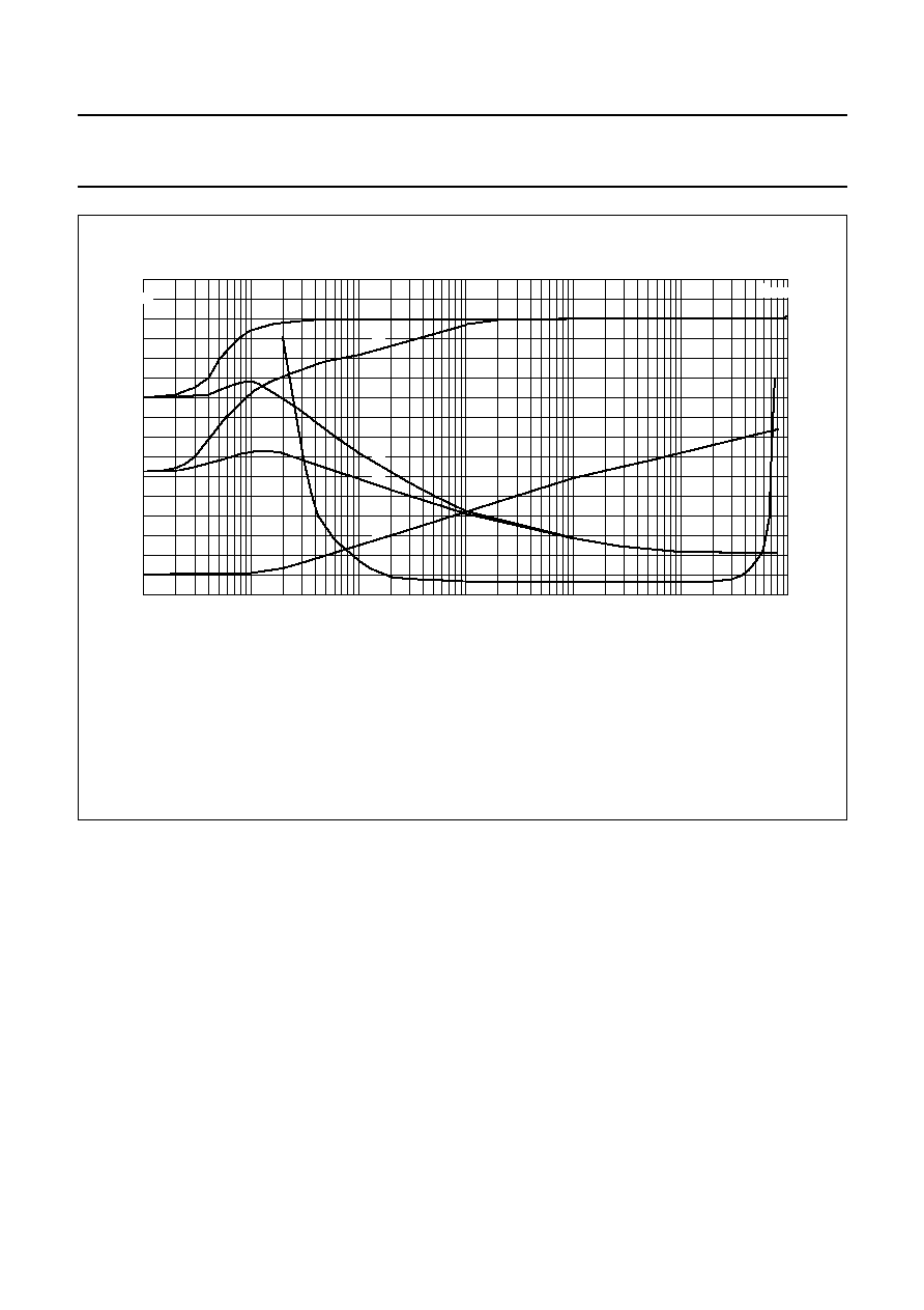
2004 Oct 21
27
Philips Semiconductors
Product specification
New In Car Entertainment car radio tuner IC with
Precision Adjacent Channel Suppression (NICE-PACS)
TEA6848H
handbook, full pagewidth
10
0
8
THD
(%)
7
6
5
4
3
2
1
0
-
70
-
60
-
50
-
40
-
30
-
20
-
10
MHC438
10
-
3
10
-
2
10
-
1
VAMIF2IN (mV)
1
(1)
(6)
10
10
2
10
3
VAMAFIF2
(dB)
(3)
(5)
(4)
(2)
Vlevel(AMFM)
(V)
Fig.3 AM detector and level output.
(1) AF: fIF = 450 kHz; m = 0.3; fmod = 1 kHz; soft mute off.
(2) AF: fIF = 450 kHz; m = 0.3; fmod = 1 kHz; soft mute on.
(3) Noise: unweighted B = 2.15 kHz; soft mute off.
(4) Noise: unweighted B = 2.15 kHz; soft mute on.
(5) Level detector output voltage, default setting.
(6) THD: m = 0.8.
2004 Oct 21
28
Philips Semiconductors
Product specification
New In Car Entertainment car radio tuner IC with
Precision Adjacent Channel Suppression (NICE-PACS)
TEA6848H
handbook, full pagewidth
6
2
0
10
-
3
10
-
2
10
-
1
1
10
10
2
10
3
MHC439
4
3
1
5
VAMIF2IN (mV)
(2)
(3)
(1)
Vlevel(AMFM)
(V)
Fig.4 AM level voltage.
(1) Level DAA setting byte 5 = FFH.
(2) Level DAA setting byte 5 = 84H (standard setting).
(3) Level DAA setting byte 5 = 00H.
handbook, full pagewidth
MHC440
1 k
1 k
100
50
100
70
71
73
77
78
14
VIFAMPIN
18
oscilloscope,
counter
8.5 V
8.5 V
test signal
4.7 nF
19
TEA6848H
Vlevel(AMFM)
Trep
VXTAL2
Vpulse
Vpulse
Fig.5 Test circuit for AM noise blanker.
Test signal: T
rep
= 2 ms, t
r
< 50 ns, t
f
< 50 ns and duty factor 50%.
V
IFAMPIN
= 4 V and V
XTAL2
= 3 V.
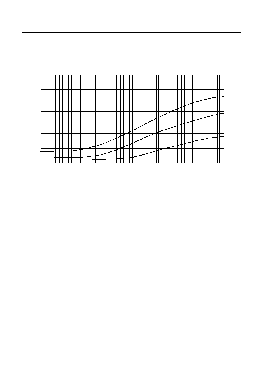
2004 Oct 21
29
Philips Semiconductors
Product specification
New In Car Entertainment car radio tuner IC with
Precision Adjacent Channel Suppression (NICE-PACS)
TEA6848H
handbook, full pagewidth
6
0
2
1
3
5
4
MHC441
10
-
3
10
-
2
10
-
1
1
10
VFMMIX2IN (mV)
10
2
10
3
(2)
(3)
Vlevel(AMFM)
(V)
(1)
Fig.6 FM level voltage.
(1) Level DAA setting byte 5 = FFH.
(2) Level DAA setting byte 5 = 84H (standard setting).
(3) Level DAA setting byte 5 = 00H.
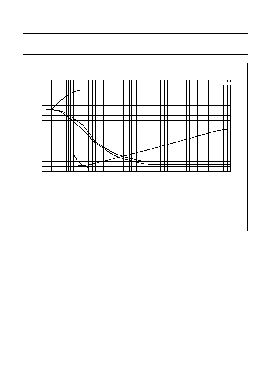
2004 Oct 21
30
Philips Semiconductors
Product specification
New In Car Entertainment car radio tuner IC with
Precision Adjacent Channel Suppression (NICE-PACS)
TEA6848H
handbook, full pagewidth
10
0
-
80
-
70
-
60
-
50
-
40
-
30
-
20
-
10
MHC442
10
-
3
10
-
2
10
-
1
VFMMIX2IN (mV)
1
10
10
2
10
3
VFMMPX;
VRDSMPX
(dB)
(2)
(1)
(4)
(3)
6
7
THD
(%)
8
9
0
2
1
3
5
4
(5)
Vlevel(AMFM)
(V)
Fig.7 (S+N)/N, THD and level voltage for FM mode as a function of FM demodulator input voltage.
(1) Output voltage for FMMPX and RDSMPX: fIF = 10.7 MHz;
f = 22.5 kHz; fmod = 1 kHz.
(2) Noise: unweighted B = 250 Hz to 15 kHz with de-emphasis 50
µ
s for FMMPX.
(3) Noise: unweighted B = 250 Hz to 15 kHz with de-emphasis 50
µ
s for RDSMPX.
(4) THD for FMMPX and RDSMPX.
(5) Level for standard setting of level DAA, byte 5 = 84H.

2004 Oct 21
31
Philips Semiconductors
Product specification
New In Car Entertainment car radio tuner IC with
Precision Adjacent Channel Suppression (NICE-PACS)
TEA6848H
12 I
2
C-BUS PROTOCOL
12.1
I
2
C-bus specification
Information about the I
2
C-bus can be found in the brochure
"The I
2
C-bus and how to use it" (order number
9398 393 40011).
The standard I
2
C-bus specification is expanded by the
following definitions.
IC addresses:
∑
1st IC address C2H: 1100001 R/W
∑
2nd IC address C0H: 1100000 R/W.
Structure of the I
2
C-bus logic: slave transceiver with auto
increment.
Subaddresses are not used.
A second I
2
C-bus address can be selected by connecting
pin FREF via a 68 k
resistor to GND.
12.1.1
D
ATA TRANSFER
Data sequence: address, byte 0, byte 1, byte 2, byte 3,
byte 4, byte 5, byte 6, and byte 7. The data transfer has to
be in this order. The LSB = 0 indicates a WRITE operation
to the TEA6848H.
Bit 7 of each byte is considered the MSB and has to be
transferred as the first bit of the byte.
The data becomes valid at the output of the internal
latches with the acknowledge of each byte. A STOP
condition after any byte can shorten transmission times.
When writing to the transceiver by using the STOP
condition before completion of the whole transfer:
∑
The remaining bytes will contain the old information
∑
If the transfer of a byte is not completed, this byte is lost
and the previous information is available.
12.1.2
I
2
C-
BUS PULL
-
UP RESISTORS
When the IC is used together with the TEA688x or
TEF689x and both SCL and SDA lines are connected via
the I
2
C-bus to the TEA688x or TEF689x, the pull-up
resistors of the tuner IC should be connected to the digital
supply voltage of the TEA688x or TEF689x. Otherwise an
I
2
C-bus pull-down can occur switching off the tuner IC
supply when the I
2
C-bus buffer interface of the TEA688x
or TEF689x is enabled for data transfer to the tuner IC.
12.1.3
F
REQUENCY SETTING
For new frequency setting, in both AM and FM mode, the
programmable divider is enabled by setting bit MUTE = 1.
To select an FM frequency, two I
2
C-bus transmissions are
necessary:
∑
First: bit MUTE = 1
∑
Second: bit MUTE = 0.
12.1.4
D
EFAULT SETTINGS
No default settings at power-on reset. One I
2
C-bus
transmission is required to program the IC.
12.1.5
T
IMING REQUIREMENTS
Table 1
Timing requirements of I
2
C-bus software
FUNCTION
TIMING
Switching from
FM to AM
400 ms (10
µ
F at pin CAGC)
Switching from
AM to FM
100 ms (10
µ
F at pin CAGC; wideband
position has to be set for at least
100 ms to activate speed-up circuitry)
Start-up in FM
mode
wideband position has to be set for at
least 100 ms to activate speed-up
circuitry
Switching to
dynamic mode
500
µ
s (18 nF at pin TACD; wideband
position has to be set for at least
500
µ
s to activate clamping circuitry at
pin TACD)

2004 Oct 21
32
Philips Semiconductors
Product specification
New In Car Entertainment car radio tuner IC with
Precision Adjacent Channel Suppression (NICE-PACS)
TEA6848H
12.2
I
2
C-bus protocol
12.2.1
D
ATA TRANSFER MODE AND
IC
ADDRESS
Table 2
Write mode
Notes
1. S = START condition.
2. A = acknowledge.
3. P = STOP condition.
Table 3
Read mode
Notes
1. S = START condition.
2. A = acknowledge.
Table 4
IC address byte
Notes
1. Defined by address pin FREF:
a) 1 = 1st IC address
b) 0 = 2nd IC address.
2. Read or write mode:
a) 0 = write operation to TEA6848H
b) 1 = read operation from TEA6848H.
12.2.2
W
RITE MODE
:
DATA BYTE
0
Table 5
Format of data byte 0
Table 6
Description of data byte 0 bits
S
(1)
address (write)
A
(2)
data byte(s)
A
(2)
P
(3)
S
(1)
address (read)
A
(2)
data byte 1
IC ADDRESS
MODE
1
1
0
0
0
0
0/1
(1)
R/W
(2)
BIT 7
BIT 6
BIT 5
BIT 4
BIT 3
BIT 2
BIT 1
BIT 0
AF
PLL14
PLL13
PLL12
PLL11
PLL10
PLL9
PLL8
BIT
SYMBOL
DESCRIPTION
7
AF
Alternative frequency. If AF = 0, then normal operation. If AF = 1, then AF (RDS)
update mode.
6 to 0
PLL[14:8]
Setting of programmable counter of synthesizer PLL. Upper byte of PLL divider
word.

2004 Oct 21
33
Philips Semiconductors
Product specification
New In Car Entertainment car radio tuner IC with
Precision Adjacent Channel Suppression (NICE-PACS)
TEA6848H
12.2.3
W
RITE MODE
:
DATA BYTE
1
Table 7
Format of data byte 1
Table 8
Description of data byte 1 bits
12.2.4
W
RITE MODE
:
DATA BYTE
2
Table 9
Format of data byte 2
Table 10 Description of data byte 2 bits
12.2.5
W
RITE MODE
:
DATA BYTE
3
Table 11 Format of data byte 3
Table 12 Description of data byte 3 bits
BIT 7
BIT 6
BIT 5
BIT 4
BIT 3
BIT 2
BIT 1
BIT 0
PLL7
PLL6
PLL5
PLL4
PLL3
PLL2
PLL1
PLL0
BIT
SYMBOL
DESCRIPTION
7 to 0
PLL[7:0]
Setting of programmable counter of synthesizer PLL. Lower byte of PLL divider
word.
BIT 7
BIT 6
BIT 5
BIT 4
BIT 3
BIT 2
BIT 1
BIT 0
MUTE
DAA6
DAA5
DAA4
DAA3
DAA2
DAA1
DAA0
BIT
SYMBOL
DESCRIPTION
7
MUTE
FM audio mute. If MUTE = 0, then FM audio not muted. If MUTE = 1, then FM audio
muted; writing to programmable divider and antenna DAA enabled.
6 to 0
DAA[6:0]
Setting of antenna digital auto alignment.
BIT 7
BIT 6
BIT 5
BIT 4
BIT 3
BIT 2
BIT 1
BIT 0
IFMT
FREF2
FREF1
FREF0
IFPR
BND1
BND0
AMFM
BIT
SYMBOL
DESCRIPTION
7
IFMT
IF measuring time. If IFMT = 0, then IF measuring time is 20 ms. If IFMT = 1, then
IF measuring time is 2 ms.
6 to 4
FREF[2:0]
Reference frequency for synthesizer. These 3 bits determine the reference
frequency, see Table 13.
3
IFPR
IF counter prescaler ratio. If IFPR = 0, then IF prescaler ratio is 40. If IFPR = 1, then
IF prescaler ratio is 10.
2 and 1
BND[1:0]
Band switch. These 2 bits select in FM mode band and local or distant, see Table 14; in
AM mode band and AM stereo, see Table 15.
0
AMFM
AM or FM switch. If AMFM = 0, then FM mode. If AMFM = 1, then AM mode.

2004 Oct 21
34
Philips Semiconductors
Product specification
New In Car Entertainment car radio tuner IC with
Precision Adjacent Channel Suppression (NICE-PACS)
TEA6848H
Table 13 Reference frequency setting
Table 14 FM mode
Table 15 AM mode
12.2.6
W
RITE MODE
:
DATA BYTE
4
Table 16 Format of data byte 4
FREF2
FREF1
FREF0
f
ref
(kHz)
0
0
0
100
1
0
0
50
0
1
0
25
1
1
0
20
0
0
1
10
1
0
1
10
0
1
1
10
1
1
1
10
BND1
BND0
FREQUENCY BAND
VCO DIVIDER
CHARGE PUMP CURRENT
0
0
FM standard
2
130
µ
A + 3 mA
0
1
FM Japan
3
130
µ
A + 3 mA
1
0
FM East Europe
3
1 mA
1
1
FM weather
1
300
µ
A
BND1
BND0
FREQUENCY BAND
VCO DIVIDER
CHARGE PUMP CURRENT
0
0
AM SW mono
10
1 mA
0
1
AM SW stereo
10
1 mA
1
0
AM LW/MW mono
20
1 mA
1
1
AM LW/MW stereo
20
1 mA
BIT 7
BIT 6
BIT 5
BIT 4
BIT 3
BIT 2
BIT 1
BIT 0
KAGC
AGC1
AGC0
AMSM/FMBW
LODX
FLAG
BW1
BW0

2004 Oct 21
35
Philips Semiconductors
Product specification
New In Car Entertainment car radio tuner IC with
Precision Adjacent Channel Suppression (NICE-PACS)
TEA6848H
Table 17 Description of data byte 4 bits
Table 18 Setting of wideband AGC for AM (m = 0.3)
Table 19 Setting of wideband AGC for FM
Table 20 FM IF2 bandwidth setting
BIT
SYMBOL
DESCRIPTION
7
KAGC
Keyed FM AGC. If KAGC = 0, then keyed FM AGC is off. If KAGC = 1, then keyed
FM AGC is on.
6 and 5
AGC[1:0]
Wideband AGC. These 2 bits set the start value of wideband AGC. For AM,
see Table 18 and for FM, see Table 19.
4
AMSM/FMBW AM soft mute or FM bandwidth. AM mode: if AMSM/FMBW = 0, then AM soft mute
is off; if AMSM/FMBW = 1, then AM soft mute is on. FM mode: see Table 20.
3
LODX
Local or distance. If LODX = 0, then distance mode is on. If LODX = 1, then local
mode is on.
2
FLAG
Software programmable flag. If FLAG = 0, then flag output pin SWFLAG is HIGH.
If FLAG = 1, then flag output pin SWFLAG is LOW.
1 and 0
BW[1:0]
FM IF2 bandwidth setting. See Table 20.
AGC1
AGC0
AM MIXER 1 INPUT VOLTAGE (PEAK VALUE)
(mV)
0
0
150
0
1
275
1
0
400
1
1
525
AGC1
AGC0
FM RF MIXER INPUT VOLTAGE (RMS VALUE)
(mV)
1
1
3
1
0
6
0
1
9
0
0
12
FMBW
BW1
BW0
FM IF2 BANDWIDTH B
-
3 dB
0
0
0
dynamic mode
0
0
1
130 kHz fixed
0
1
0
90 kHz fixed
0
1
1
60 kHz fixed
1
0
0
25 kHz frequency offset alignment mode; bandwidth flag output
switched to frequency offset detector alignment voltage

2004 Oct 21
36
Philips Semiconductors
Product specification
New In Car Entertainment car radio tuner IC with
Precision Adjacent Channel Suppression (NICE-PACS)
TEA6848H
12.2.7
W
RITE MODE
:
DATA BYTE
5
Table 21 Format of data byte 5
Table 22 Description of data byte 5 bits
Table 23 Standard setting of data byte 5 bits
12.2.8
W
RITE MODE
:
DATA BYTE
6
Table 24 Format of data byte 6
Table 25 Description of data byte 6 bits
12.2.9
W
RITE MODE
:
DATA BYTE
7
Table 26 Format of data byte 7
Table 27 Description of data byte 7 bits
BIT 7
BIT 6
BIT 5
BIT 4
BIT 3
BIT 2
BIT 1
BIT 0
LST4
LST3
LST2
LST1
LST0
LSL2
LSL1
LSL0
BIT
SYMBOL
DESCRIPTION
7 to 3
LST[4:0]
Setting of level DAA starting point. These 5 bits determine the offset of the level
detector output voltage.
2 to 0
LSL[2:0]
Setting of level DAA slope. These 3 bits determine the steepness of the level detector
output voltage.
SETTING OF LEVEL DAA STARTING POINT
SETTING OF LEVEL DAA SLOPE
LST4
LST3
LST2
LST1
LST0
LSL2
LSL1
LSL0
1
0
0
0
0
1
0
0
BIT 7
BIT 6
BIT 5
BIT 4
BIT 3
BIT 2
BIT 1
BIT 0
TE
CF6
CF5
CF4
CF3
CF2
CF1
CF0
BIT
SYMBOL
DESCRIPTION
7
TE
Threshold extension. If TE = 0, then threshold extension is off. If TE = 1, then
threshold extension is on.
6 to 0
CF[6:0]
Setting of FM IF2 centre frequency DAA. The content of CF6 to CF0 determines the
centre frequency of the 450 kHz filter.
BIT 7
BIT 6
BIT 5
BIT 4
BIT 3
BIT 2
BIT 1
BIT 0
FOF3
FOF2
FOF1
FOF0
FGN3
FGN2
FGN1
FGN0
BIT
SYMBOL
DESCRIPTION
7 to 4
FOF[3:0]
Frequency offset gain alignment.
3 to 0
FGN[3:0]
IF2 filter gain alignment.

2004 Oct 21
37
Philips Semiconductors
Product specification
New In Car Entertainment car radio tuner IC with
Precision Adjacent Channel Suppression (NICE-PACS)
TEA6848H
12.2.10 R
EAD MODE
:
DATA BYTE
0
Table 28 Format of 1st data byte
Table 29 Description of data byte 0 bits
13 TEST AND APPLICATION INFORMATION
Table 30 List of components for test and application circuits (Figs 8, 9, 10 and 11)
BIT 7
BIT 6
BIT 5
BIT 4
BIT 3
BIT 2
BIT 1
BIT 0
IFC7
IFC6
IFC5
IFC4
IFC3
IFC2
IFC1
IFC0
BIT
SYMBOL
DESCRIPTION
7 to 0
IFC[7:0]
IF counter result. These bits contain the least significant eight bits of the IF counter
result.
SYMBOL
PARAMETER
TYPE
MANUFACTURER
C1
capacitor for VCO tuning
270 pF; type NP0
-
L1
10.7 MHz IF coil
P7 PSG P826RC 5134N=S
TOKO
L2
450 kHz IF coil
P7PSGAE-5078D=S
TOKO
L3
oscillator coil
E543SNAS-02010
TOKO
L4
FM image rejection
611SNS-1066Y
TOKO
L5
FM input transformer
369INS-3076X
TOKO
L6
FM antenna coil
LQN1HR50; 215 nH
MURATA
L7
PIN diode bias
LQN1HR21; 500 nH
MURATA
L8
connection image reject
wire 10 mm/printed coil
-
L9
AM input
388BN-1211Z
TOKO
R4
resistor for stabilizer
3.3 k
; RC12G
BC Components
-
crystal 20.5 MHz
LN-G102-587
NDK

2004 Oct 21
38
Philips Semiconductors
Product specification
New In Car Entertainment car radio tuner IC with
Precision Adjacent Channel Suppression (NICE-PACS)
TEA6848H
handbook, full pagewidth
DAA
VCO
AM
MIXER 1
AM
MIXER 2
AM
AGC
90
∞
FM
I/Q MIXER 1
FM
AGC
TUNING SYSTEM
AM-NOISE
DETECTOR
PEAK/
AVERAGE
BLANK
PULSE
˜
10/
˜
20
˜
1/
˜
2/
˜
3
90
∞
TEA6848H
FM
MIXER 2
˜
2
19
18
15
14
13 12 11
10 9
8 7
6
5
20
22
23
24
25
26
27
28
29
30
31
32
33
34
35
36
37
38
39
40
41
42
43
44
45 46
47
48
49
50
51
AM
LEVEL
LEVEL
BB156
Vtune
fref
PLL
DGND
22
1
nF
C1
4.7 k
100 nF
10 k
2.2 k
1.2 k
3.9
nF
100 nF
1.8
pF
2.7
pF
22
22
nF
L3
3.3
nF
SFE 10.7
MS3
22
22 nF
L1
SFE 10.7
MS3
WB/JAPAN/OIRT
21
SW CONTROL
FLAG
17
16
47
µ
F
100
nF
220
nF
22
nF
22
22
nF
22 nF
22
22 nF
VDDD
ANTENNA
RFGND
4:6
22
L5
BB814
22 k
L4
BAS16
WB FLAG
BAV99
10 nF
1 nF
270
BAQ806
220
nF
antenna
2.2 M
5 V
L8
18 pF
215
nH
6.8 pF
1
pF
12
pF
500 nH
1
nF
10
µ
F
1
nF
1
nF
2.2
k
330
BA595
100 nF
22
220
nF
BC847C
1.8 M
150
pF
820
µ
H
560
2.2 nF
56
µ
H
470
µ
H
100 nF
BF862
2.2
M
10 nF
6.8
µ
H
1
µ
F
1
µ
F
L9
10
k
22 nF
22
µ
F
220 nF
270
pF
100 k
L7
L6
+
+
+
I
2
C-bus
I
2
C-bus
I
2
C-bus
I
2
C-bus
I
2
C-bus
+
+
◊
◊
◊
◊
MHC443
A
B
C
D
E
F
G
H
I
L
M
N
K
J
Fig.8 Application diagram (continued in Fig.9).
For list of components see Table 30.
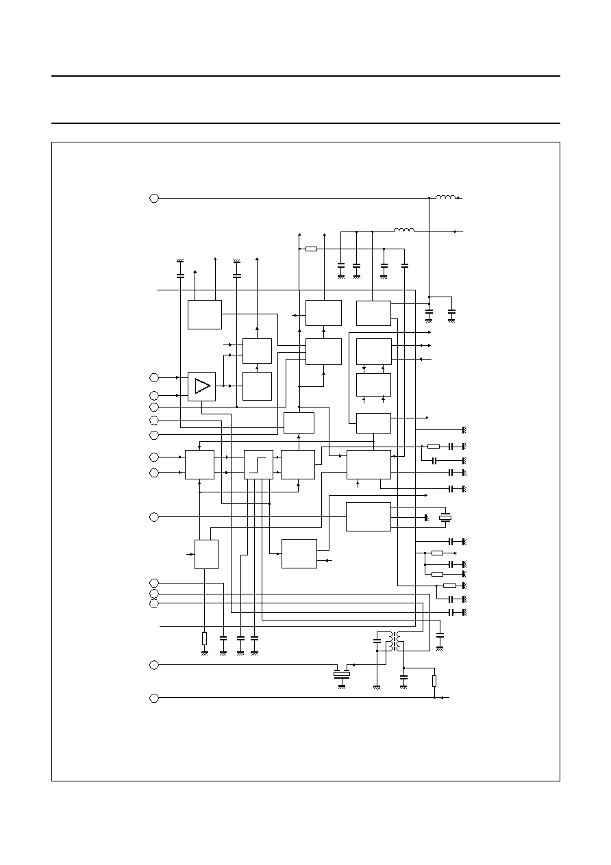
2004 Oct 21
39
Philips Semiconductors
Product specification
New In Car Entertainment car radio tuner IC with
Precision Adjacent Channel Suppression (NICE-PACS)
TEA6848H
handbook, full pagewidth
RDS
UPDATE
CRYSTAL
OSCILLATOR
POWER
SUPPLY
LEVEL
DAA
IF
COUNT
AM
DEMOD
MUX
IF
FILTER
FM
DEMOD
STABI
BUFFER
BANDWIDTH
CONTROL
x1/ x15
AMPLIFIER
MPXOUT
20.5 MHz
4
3
2
1
52
53
54
55
56
57
58
59
60
61
62
63
64
65
66
67
68
69
70
71
72
73
74
75
76
77
78
79
80
WB
LEVEL
FM
AM
SAMPLE
AF
HOLD
AF
5 V
AUDIO/IF
AM
RDS/
MPX
MPX
FM
3.3
µ
H
3.3
µ
H
100
nF
100
nF
8.5 V
IFBWFLAG
SCL
SDA
VIFBW
V
level(AMFM)
20.5
MHz
22
22 nF
L2
SFR450H
8.5 V
IF2GND
VDDA5
5 V
220 nF
6.8
nF
12 k
47
µ
F
1
nF
200
nF
47
µ
F
390
8.2 nF
33 nF
8.2 nF
33 nF
10 k
820
120 k
22 nF
10
µ
F
220 nF
47 nF
47
47 nF
nF
22
nF
R4
3.3 k
VDDA6
VDDA5
AM STEREO
MUTE
RDS
270 pF
I
2
C-bus
I
2
C-BUS
I
2
C-bus
+
+
+
MHC444
A
B
C
D
E
F
G
H
I
L
M
N
K
J
TEA6848H
Fig.9 Application diagram (continued from Fig.8).
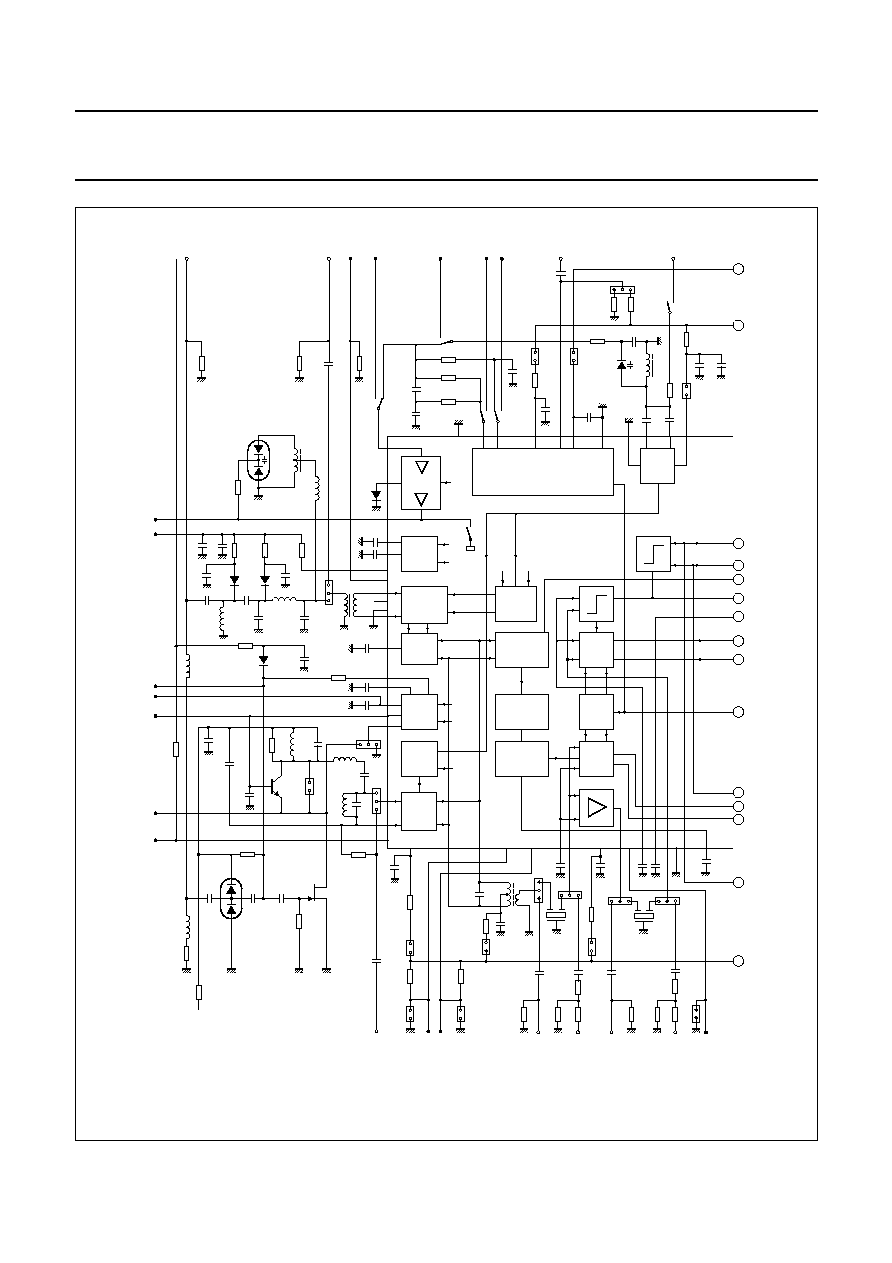
2004 Oct 21
40
Philips Semiconductors
Product specification
New In Car Entertainment car radio tuner IC with
Precision Adjacent Channel Suppression (NICE-PACS)
TEA6848H
handbook, full pagewidth
DAA
VCO
AM
MIXER 1
AM
MIXER 2
AM
AGC
90
∞
FM
I/Q MIXER 1
FM
AGC
TUNING SYSTEM
AM-NOISE
DETECTOR
PEAK/
AVERAGE
BLANK
PULSE
˜
10/
˜
20
˜
1/
˜
2/
˜
3
90
∞
TEA6848H
FM
MIXER 2
˜
2
19
18
15
14
13 12 11
10 9
8 7
6
5
20
22
23
24
25
26
27
28
29
30
31
32
33
34
35
36
37
38
39
40
41
42
43
44
45 46
47
48
49
50
51
AM
LEVEL
LEVEL
WB/JAPAN/OIRT
21
17
16
ANTENNA
I
2
C-bus
I
2
C-bus
I
2
C-bus
I2C-bus
I
2
C-bus
◊
◊
◊
◊
MHC445
A
B
C
D
E
F
G
H
I
L
M
N
O
K
J
BB156
Vtune
DGND
22
4.7 k
22
1.2 k
2.2 k
10 k
4.7
k
0
1
nF
270 pF
100 nF
3.9 nF
100 nF
1.8
pF
2.7
pF
22
nF
L3
C1
3.3
nF
SFE10.7
MS3
I-centre
test mode
frequency
22
nF
L1
SFE 10.7
MS3
filter
Q
I
IF1GND
47
µ
F
100
nF
220 nF
22
22
nF
22
nF
22
nF
22
nF
fref
PLL
100 nF
100 nF
100 nF
100 nF
2
2
304
304
52
52
330
330
AM RF
FMIF1
output
IF
output
FMIF2
input
IF
input
100 nF
100 k
68 k
relay 3
relay 2
relay 1
relay 1
RFGND
4:6
L5
BB814
L4
L8
BAS16
WB FLAG
antenna
input
FM RF
input
100
nF
WB
FLAG
1
µ
F
1
µ
F
10
k
VCC1 8.5 V
5 V
analog
BAV99
10 nF
1 nF
270
22
BAQ806
220
nF
SW
FLAG
100 nF
220
nF
BC847C
1.8 M
2.2 M
10 k
22
68 k
22
22
68 k
150 pF
820
µ
H
56
µ
H
470
µ
H
560
47
2.2 nF
BF862
10 nF
L9
22 nF
22
µ
F
220 nF
270
pF
CONTROL
18 pF
215
nH
6.8 pF
1 pF
12
pF
500 nH
1
nF
10
µ
F
1
nF
1 nF
2.2
k
330
22
BA595
L7
L6
6.8
µ
H
100
nF
100 nF
Q
I
+
+
+
+
input
output
test
mode
input
+
2.2 M
22 k
47
Fig.10 Test circuit (continued in Fig.11).
For list of components see Table 30.

2004 Oct 21
41
Philips Semiconductors
Product specification
New In Car Entertainment car radio tuner IC with
Precision Adjacent Channel Suppression (NICE-PACS)
TEA6848H
handbook, full pagewidth
RDS
UPDATE
CRYSTAL
OSCILLATOR
POWER
SUPPLY
LEVEL
DAA
IF
COUNT
AM
DEMOD
MUX
IF
FILTER
FM
DEMOD
STABI
BUFFER
BANDWIDTH
CONTROL
x1/ x15
AMPLIFIER
MPXOUT
20.5 MHz
4
3
2
1
52
53
54
55
56
57
58
59
60
61
62
63
64
65
66
67
68
69
70
71
72
73
74
75
76
77
78
79
80
WB
LEVEL
FM
AM
IFBWFLAG
SCL
SDA
20.5
MHz
22
22 nF
L2
100 nF
jumper
test pin and STOCKO connector
coaxial connector (SMC)
100 nF
2 k
47
SFR450H
IF2GND
390
8.2 nF
22 nF
22 nF
8.2 nF
8.2 nF
R76 120 k
10
µ
F
220 nF
47 nF
47
47 nF
nF
22
nF
R4
3.3 k
AM STEREO
MUTE
RDS
270 pF
I
2
C-bus
I
2
C-BUS
I
2
C-bus
+
+
MHC446
68 k
(1.5 k
)
100
nF
100
nF
100
nF
68 k
(1.5 k
)
10 k
10 k
56 k
10 k
820
10 k
47
µ
F
47
µ
F
220
nF
6.8
nF
100
nF
100
nF
47
µ
F
47
µ
F
47
µ
F
3.3
µ
H
3.3
µ
H
3.3
µ
H
100 nF
100 nF
100 nF
SDA
SCL
DGND
I
2
C-bus interface
330
pF
200
nF
2 k
B
A
C
D
E
F
G
H
I
J
M
N
O
L
K
AM IF2
AM IF
output
input
SAMPLE
AF
HOLD
AF
AUDIO/IF
AM
RDS/
MPX
MPX
FM
+
+
+
+
TEA6848H
Fig.11 Test circuit (continued from Fig.10).

2004 Oct 21
42
Philips Semiconductors
Product specification
New In Car Entertainment car radio tuner IC with
Precision Adjacent Channel Suppression (NICE-PACS)
TEA6848H
Table 31 DC operating points
SYMBOL
PIN
UNLOADED DC VOLTAGE (V)
AM MODE
FM MODE
MIN.
TYP.
MAX.
MIN.
TYP.
MAX.
FMLIMDCFDB1
1
floating
3.7
4.2
4.8
FMLIMDCFDB2
2
floating
3.7
4.2
4.8
AMIF2DEC
3
2.4
2.7
3.2
floating
IREFFMIF2
4
0
0.4
0.55
0.7
AMNBHOLD
5
4.3
4.6
5.1
8
8.4
-
AMIF2IN
6
2.4
2.7
3.2
floating
IF1GND
7
external 0
external 0
FMMIX2IN
8
0
0.1
-
1.5
1.8
2.1
COFFSET
9
floating
3.5
4
4.5
FMMIX2DEC
10
0
0.1
-
1.5
1.8
2.1
IFCDAATEST
11
0
0
IFAMPOUT
12
7.2
7.9
-
2.4
3
3.6
V
DDA1
13
external 8.5
external 8.5
IFAMPIN
14
2.4
2.7
3
1.5
2
2.5
IFAMPDEC
15
2.4
2.7
3
1.5
2
2.5
IF2FILQ
16
0
0
IF2FILI
17
0
0
MIX1OUT1
18
external 8.5
external 8.5
MIX1OUT2
19
external 8.5
external 8.5
V
DDA2
20
external 8.5
external 8.5
SWFLAG
21
open-collector
AMMIX1DEC
22
2.3
2.75
3.1
floating
AMMIX1IN
23
2.3
2.75
3.1
floating
VAMCASFB
24
3.7
4.3
4.9
0
0.1
0.2
VAMCAS
25
4.5
5
5.5
0
0.1
1
TAFAMAGC
26
0
2.8
4.6
0 (no WB)
0.3 (no WB)
0.5 (no WB)
THFAMAGC
27
2.5
2.8
3.1
floating
IAMAGC
28
8.5 (external biasing)
1
2
3
V
ref(MIX)
29
2.7
3.1
3.4
6.5
7.1
7.9
FMMIXIN1
30
1
1.3
1.6
2.3
2.8
3.3
RFGND
31
external 0
external 0
i.c.
32
-
-
FMMIXIN2
33
1
1.3
1.6
2.3
2.8
3.3
WBFLAG
34
0
4 (WB)
4.5 (WB)
5 (WB)
-
(FM)
<0.5 (FM)
-
(FM)
IFMAGC
35
5 (external application)
0.1 (external
biasing)
-
4 (external
biasing)

2004 Oct 21
43
Philips Semiconductors
Product specification
New In Car Entertainment car radio tuner IC with
Precision Adjacent Channel Suppression (NICE-PACS)
TEA6848H
TFMAGC
36
7.5
8
8.3
3.9
4.6
5.3
TKEYEDAGC
37
floating
1
-
7
DAAOUT
38
-
0.2
0.3
0.2
-
8.25
DAATD
39
floating
0.2
-
1.5
DAAIN
40
0
-
8.5
0
-
8.5
i.c.
41
-
-
V
tune
42
0
-
8.5
0
-
8.5
CPOUT
43
0
-
8.5
0
-
8.5
V
DDA3
44
external 8.5
external 8.5
FREF
45
3.2
3.4
3.7
3.2
3.4
3.7
V
DDD
46
external 5
external 5
DGND
47
external 0
external 0
VCOGND
48
external 0
external 0
OSCFDB
49
2.2
2.8
3.4
2.2
2.8
3.4
OSCTNK
50
5
6.1
7.2
5
6.1
7.2
V
DDA4
51
external 8.5
external 8.5
MPXDCFDB
52
-
2
2.4
2.8
AFSAMPLE
53
0
0.2
0.5
0
0.2
0.5
AFHOLD
54
open-collector 5
open-collector
TRDSMUTE
55
1.7
2.2
2.7
0.7 (muted)
1.2 (muted)
1.7 (muted)
5.2 (not muted) 5.7 (not muted) 6.2 (not muted)
AMAFIF2
56
4
4.3
4.6
floating 3.3
RDSMPX
57
0
3.2
4
4.8
FMMPX
58
0
0.5
1
3.2
4
4.8
V
DDA5
59
external 5
external 5
MODDET
60
0
2
2.5
3
V
DDA6
61
external 8.5
external 8.5
IFBWFLAG
62
open-collector 8.5
3 (IFBW = 1)
3.3 (IFBW = 1)
4.1 (IFBW = 1)
SDA
63
4.8
5
5.2
4.8
5
5.2
SCL
64
4.8
5
5.2
4.8
5
5.2
V
IFBW
65
0
0.1
-
0.5
-
4
IF2GND
66
external 0
external 0
CINT
67
0
3.2
4
4.8
MODETOUT
68
0
2
3
4
TACD
69
0
3.2
3.6
4
V
level(AMFM)
70
0
-
7
0
-
7
XTAL1
71
1.7
2.1
2.5
1.7
2.1
2.5
XTALGND
72
external 0
external 0
SYMBOL
PIN
UNLOADED DC VOLTAGE (V)
AM MODE
FM MODE
MIN.
TYP.
MAX.
MIN.
TYP.
MAX.
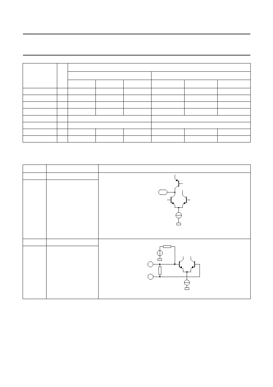
2004 Oct 21
44
Philips Semiconductors
Product specification
New In Car Entertainment car radio tuner IC with
Precision Adjacent Channel Suppression (NICE-PACS)
TEA6848H
14 INTERNAL CIRCUITRY
Table 32 Equivalent pin circuits
XTAL2
73
1.7
2.1
2.5
1.7
2.1
2.5
V
level(ACD)
74
0.5
1
2
0.3
0.5
0.8
ACDTHRES
75
0.37
-
0.4
0.37
-
0.4
IREF
76
4
4.25
4.5
4
4.25
4.5
AMMIX2OUT1
77
external 8.5
external 8.5
AMMIX2OUT2
78
external 8.5
external 8.5
CAGC
79
3.6
4.3
4.8
1.7
2.5
3.3
V
ref(lim)
80
0.5
0.8
1.2
3.6
4.2
4.8
PIN
SYMBOL
EQUIVALENT CIRCUIT
1
FMLIMDCFDB1
2
FMLIMDCFDB2
3
AMIF2DEC
6
AMIF2IN
SYMBOL
PIN
UNLOADED DC VOLTAGE (V)
AM MODE
FM MODE
MIN.
TYP.
MAX.
MIN.
TYP.
MAX.
MDB088
1, 2
2 k
3
6
500
MHC375
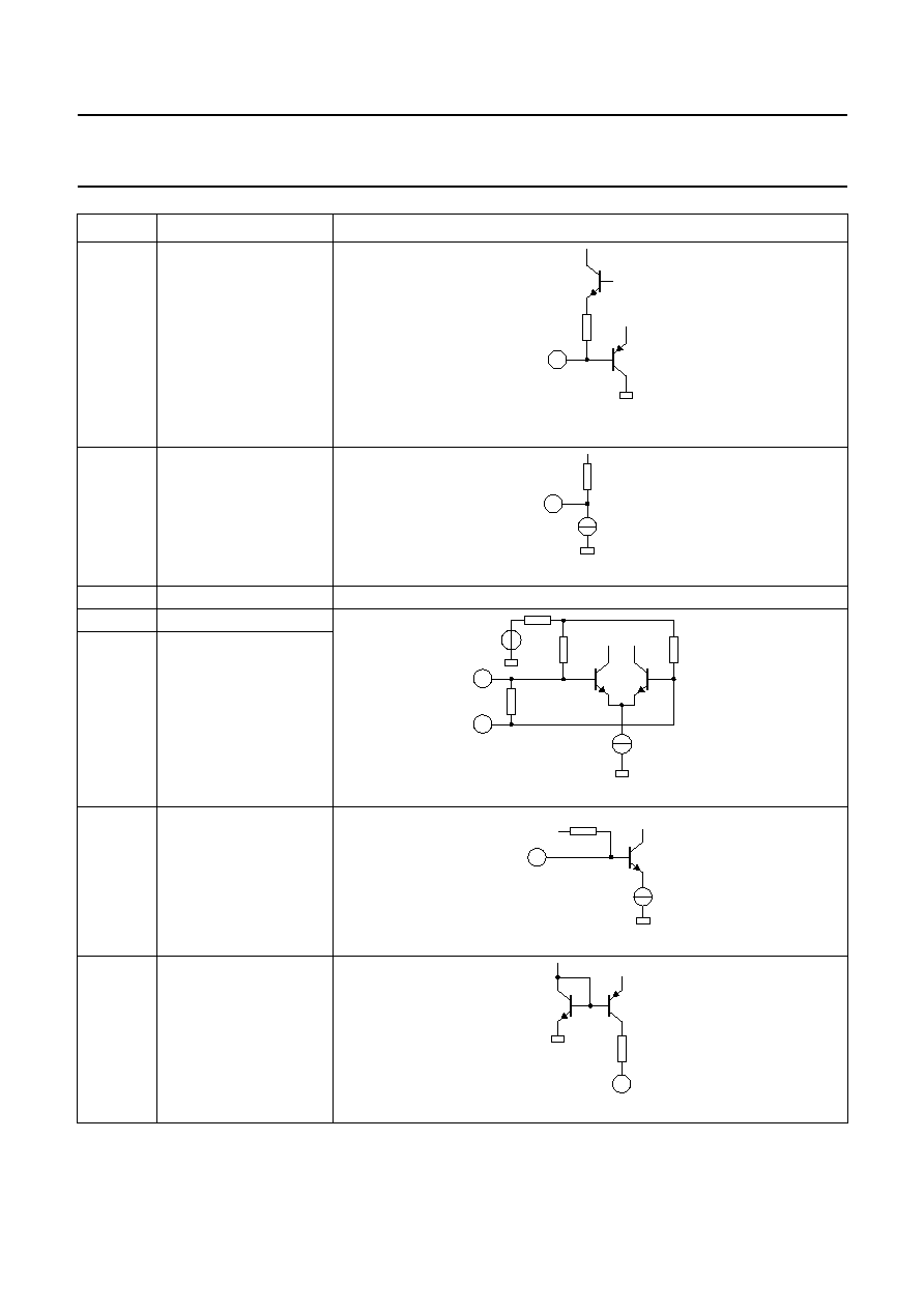
2004 Oct 21
45
Philips Semiconductors
Product specification
New In Car Entertainment car radio tuner IC with
Precision Adjacent Channel Suppression (NICE-PACS)
TEA6848H
4
IREFFMIF2
5
AMNBHOLD
7
IF1GND
8
FMMIX2IN
10
FMMIX2DEC
9
COFFSET
11
IFCDAATEST
PIN
SYMBOL
EQUIVALENT CIRCUIT
MDB089
4
80 k
5
MHC377
MDB090
10
8
350
4 k
4 k
9
1 M
MHC379
11
MHC453
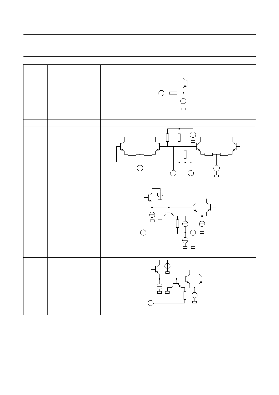
2004 Oct 21
46
Philips Semiconductors
Product specification
New In Car Entertainment car radio tuner IC with
Precision Adjacent Channel Suppression (NICE-PACS)
TEA6848H
12
IFAMPOUT
13
V
DDA1
14
IFAMPIN
15
IFAMPDEC
16
IF2FILQ
17
IF2FILI
PIN
SYMBOL
EQUIVALENT CIRCUIT
12
330
MHC381
MDB091
14
330
5
k
5
k
15
16
MHC455
17
MHC454

2004 Oct 21
47
Philips Semiconductors
Product specification
New In Car Entertainment car radio tuner IC with
Precision Adjacent Channel Suppression (NICE-PACS)
TEA6848H
18
MIX1OUT1
19
MIX1OUT2
20
V
DDA2
21
SWFLAG
22
AMMIX1DEC
23
AMMIX1IN
24
VAMCASFB
25
VAMCAS
PIN
SYMBOL
EQUIVALENT CIRCUIT
19
18
MHC383
21
MHC384
23
22
400
MHC385
24
10 k
MHC447
25
1 k
MHC448
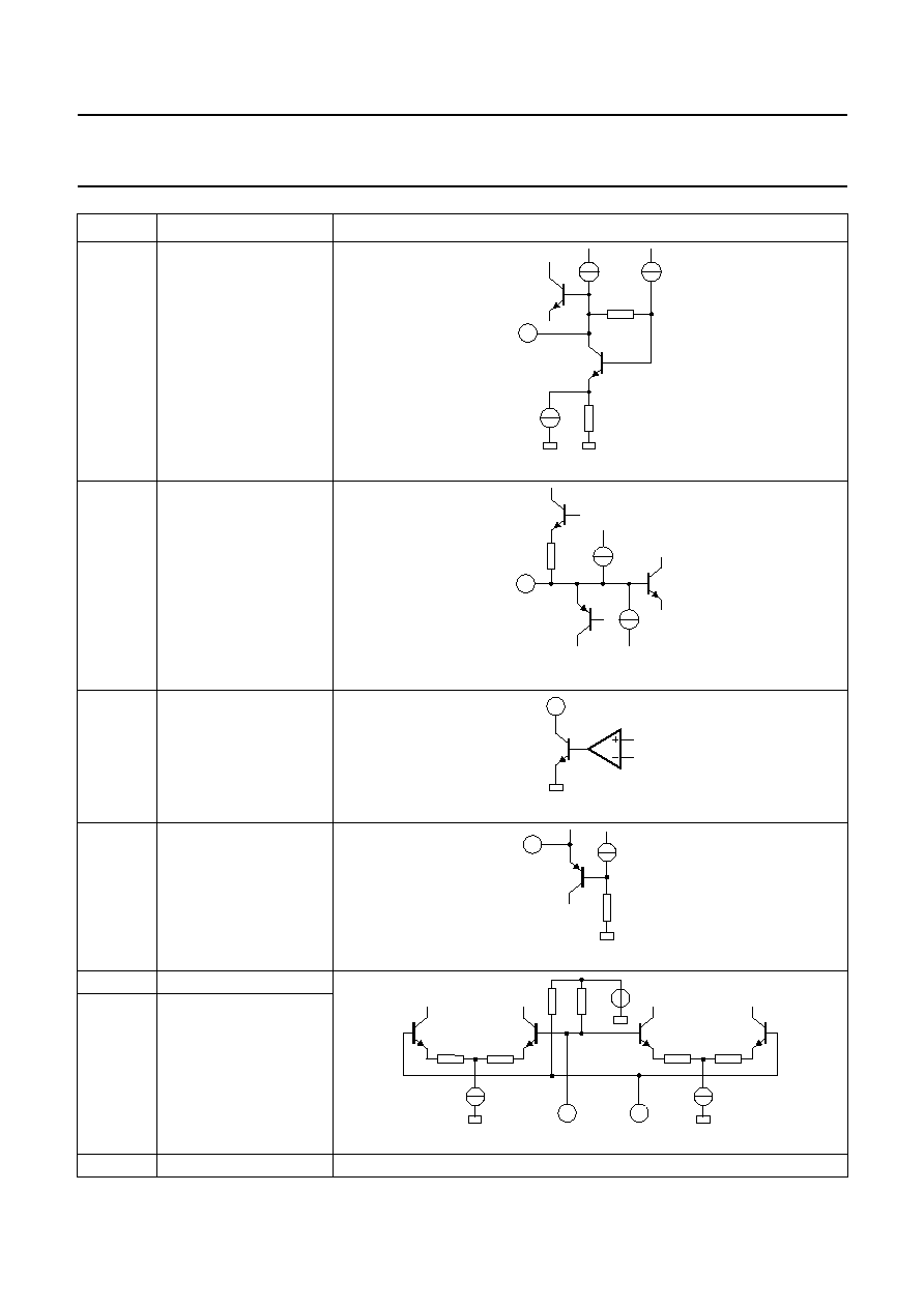
2004 Oct 21
48
Philips Semiconductors
Product specification
New In Car Entertainment car radio tuner IC with
Precision Adjacent Channel Suppression (NICE-PACS)
TEA6848H
26
TAFAMAGC
27
THFAMAGC
28
IAMAGC
29
V
ref(MIX)
30
FMMIXIN1
33
FMMIXIN2
31
RFGND
PIN
SYMBOL
EQUIVALENT CIRCUIT
MDB100
26
MDB101
27
28
MHC388
29
MHC389
33
30
10
k
10
k
MHC390

2004 Oct 21
49
Philips Semiconductors
Product specification
New In Car Entertainment car radio tuner IC with
Precision Adjacent Channel Suppression (NICE-PACS)
TEA6848H
32
i.c.
34
WBFLAG
35
IFMAGC
36
TFMAGC
37
TKEYEDAGC
38
DAAOUT
PIN
SYMBOL
EQUIVALENT CIRCUIT
34
200
50 k
MHC391
35
MHC392
10 k
36
10 k
MHC393
5 k
37
MHC394
38
36
k
MHC395

2004 Oct 21
50
Philips Semiconductors
Product specification
New In Car Entertainment car radio tuner IC with
Precision Adjacent Channel Suppression (NICE-PACS)
TEA6848H
39
DAATD
40
DAAIN
41
i.c.
42
V
tune
43
CPOUT
44
V
DDA3
PIN
SYMBOL
EQUIVALENT CIRCUIT
39
MHC396
3
9
43
40
2.5 k
MHC397
42
MHC398
3
9
40
43
MHC399
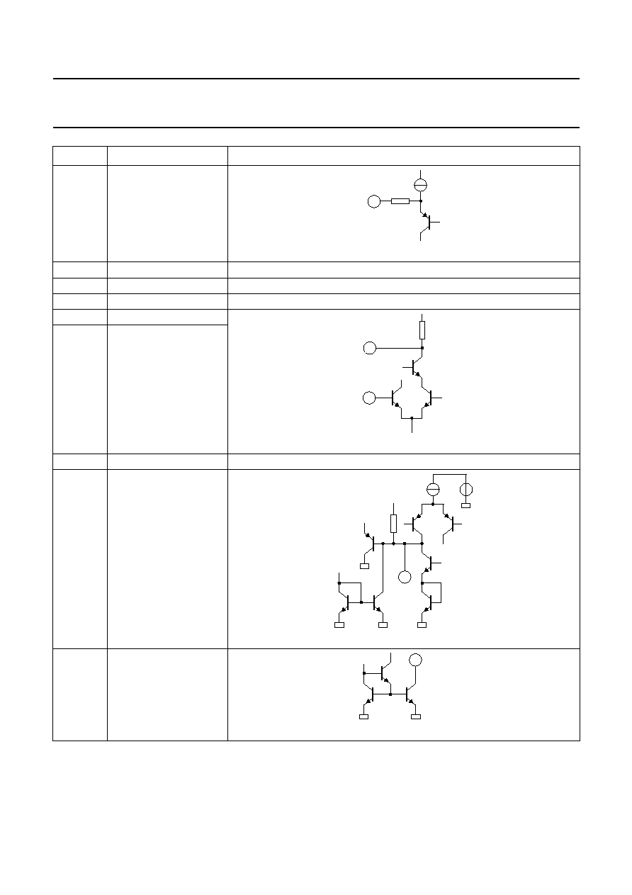
2004 Oct 21
51
Philips Semiconductors
Product specification
New In Car Entertainment car radio tuner IC with
Precision Adjacent Channel Suppression (NICE-PACS)
TEA6848H
45
FREF
46
V
DDD
47
DGND
48
VCOGND
49
OSCFDB
50
OSCTNK
51
V
DDA4
52
MPXDCFDB
53
AFSAMPLE
PIN
SYMBOL
EQUIVALENT CIRCUIT
45
1 k
MHC400
49
3 k
50
MHC401
52
MHC449
53
MHC402
2004 Oct 21
52
Philips Semiconductors
Product specification
New In Car Entertainment car radio tuner IC with
Precision Adjacent Channel Suppression (NICE-PACS)
TEA6848H
54
AFHOLD
55
TRDSMUTE
56
AMAFIF2
57
RDSMPX
PIN
SYMBOL
EQUIVALENT CIRCUIT
54
MHC403
55
MHC404
56
201 k
0.35 pF
MHC405
MDB102
300
57
2004 Oct 21
53
Philips Semiconductors
Product specification
New In Car Entertainment car radio tuner IC with
Precision Adjacent Channel Suppression (NICE-PACS)
TEA6848H
58
FMMPX
59
V
DDA5
60
MODDET
61
V
DDA6
62
IFBWFLAG
63
SDA
PIN
SYMBOL
EQUIVALENT CIRCUIT
MDB103
280
58
MDB104
60
MDB095
1 k
50
µ
A
62
62
FM (FMBW = 1)
AM
63
1 k
MHC410
2004 Oct 21
54
Philips Semiconductors
Product specification
New In Car Entertainment car radio tuner IC with
Precision Adjacent Channel Suppression (NICE-PACS)
TEA6848H
64
SCL
65
V
IFBW
66
IF2GND
67
CINT
68
MODETOUT
69
TACD
PIN
SYMBOL
EQUIVALENT CIRCUIT
64
1 k
MHC411
MDB096
65
MDB097
67
68
MHC450
69
2 k
MHC451
2004 Oct 21
55
Philips Semiconductors
Product specification
New In Car Entertainment car radio tuner IC with
Precision Adjacent Channel Suppression (NICE-PACS)
TEA6848H
70
V
level(AMFM)
71
XTAL1
72
XTALGND
73
XTAL2
74
V
level(ACD)
75
ACDTHRES
PIN
SYMBOL
EQUIVALENT CIRCUIT
70
150
MHC414
73
72
71
27.6 pF
10 k
20 k
27.6 pF
20 k
10 k
MHC415
MDB212
74
8 k
MDB099
75
2004 Oct 21
56
Philips Semiconductors
Product specification
New In Car Entertainment car radio tuner IC with
Precision Adjacent Channel Suppression (NICE-PACS)
TEA6848H
76
IREF
77
AMMIX2OUT1
78
AMMIX2OUT2
PIN
SYMBOL
EQUIVALENT CIRCUIT
76
10 k
MHC418
78
77
MHC419
2004 Oct 21
57
Philips Semiconductors
Product specification
New In Car Entertainment car radio tuner IC with
Precision Adjacent Channel Suppression (NICE-PACS)
TEA6848H
79
CAGC
80
V
ref(lim)
PIN
SYMBOL
EQUIVALENT CIRCUIT
MDB092
79
AM
79
420
10 k
FM
80
MHC452

2004 Oct 21
58
Philips Semiconductors
Product specification
New In Car Entertainment car radio tuner IC with
Precision Adjacent Channel Suppression (NICE-PACS)
TEA6848H
15 PACKAGE OUTLINE
UNIT
A
max.
A
1
A
2
A
3
b
p
c
E
(1)
e
H
E
L
L
p
Z
y
w
v
REFERENCES
OUTLINE
VERSION
EUROPEAN
PROJECTION
ISSUE DATE
IEC
JEDEC
JEITA
mm
1.6
0.16
0.04
1.5
1.3
0.25
0.27
0.13
0.18
0.12
12.1
11.9
0.5
14.15
13.85
1.45
1.05
7
0
o
o
0.15
0.1
0.2
1
DIMENSIONS (mm are the original dimensions)
Note
1. Plastic or metal protrusions of 0.25 mm maximum per side are not included.
0.75
0.30
SOT315-1
136E15
MS-026
00-01-19
03-02-25
D
(1)
(1)
(1)
12.1
11.9
H
D
14.15
13.85
E
Z
1.45
1.05
D
b
p
e
E
A
1
A
L
p
detail X
L
(A )
3
B
20
c
D
H
b
p
E
H
A
2
v
M
B
D
Z D
A
Z E
e
v
M
A
X
1
80
61
60
41
40
21
y
pin 1 index
w
M
w
M
0
5
10 mm
scale
LQFP80: plastic low profile quad flat package; 80 leads; body 12 x 12 x 1.4 mm
SOT315-1

2004 Oct 21
59
Philips Semiconductors
Product specification
New In Car Entertainment car radio tuner IC with
Precision Adjacent Channel Suppression (NICE-PACS)
TEA6848H
16 SOLDERING
16.1
Introduction to soldering surface mount
packages
This text gives a very brief insight to a complex technology.
A more in-depth account of soldering ICs can be found in
our
"Data Handbook IC26; Integrated Circuit Packages"
(document order number 9398 652 90011).
There is no soldering method that is ideal for all surface
mount IC packages. Wave soldering can still be used for
certain surface mount ICs, but it is not suitable for fine pitch
SMDs. In these situations reflow soldering is
recommended.
16.2
Reflow soldering
Reflow soldering requires solder paste (a suspension of
fine solder particles, flux and binding agent) to be applied
to the printed-circuit board by screen printing, stencilling or
pressure-syringe dispensing before package placement.
Driven by legislation and environmental forces the
worldwide use of lead-free solder pastes is increasing.
Several methods exist for reflowing; for example,
convection or convection/infrared heating in a conveyor
type oven. Throughput times (preheating, soldering and
cooling) vary between 100 and 200 seconds depending
on heating method.
Typical reflow peak temperatures range from
215 to 270
∞
C depending on solder paste material. The
top-surface temperature of the packages should
preferably be kept:
∑
below 225
∞
C (SnPb process) or below 245
∞
C (Pb-free
process)
≠ for all BGA, HTSSON-T and SSOP-T packages
≠ for packages with a thickness
2.5 mm
≠ for packages with a thickness < 2.5 mm and a
volume
350 mm
3
so called thick/large packages.
∑
below 240
∞
C (SnPb process) or below 260
∞
C (Pb-free
process) for packages with a thickness < 2.5 mm and a
volume < 350 mm
3
so called small/thin packages.
Moisture sensitivity precautions, as indicated on packing,
must be respected at all times.
16.3
Wave soldering
Conventional single wave soldering is not recommended
for surface mount devices (SMDs) or printed-circuit boards
with a high component density, as solder bridging and
non-wetting can present major problems.
To overcome these problems the double-wave soldering
method was specifically developed.
If wave soldering is used the following conditions must be
observed for optimal results:
∑
Use a double-wave soldering method comprising a
turbulent wave with high upward pressure followed by a
smooth laminar wave.
∑
For packages with leads on two sides and a pitch (e):
≠ larger than or equal to 1.27 mm, the footprint
longitudinal axis is preferred to be parallel to the
transport direction of the printed-circuit board;
≠ smaller than 1.27 mm, the footprint longitudinal axis
must be parallel to the transport direction of the
printed-circuit board.
The footprint must incorporate solder thieves at the
downstream end.
∑
For packages with leads on four sides, the footprint must
be placed at a 45
∞
angle to the transport direction of the
printed-circuit board. The footprint must incorporate
solder thieves downstream and at the side corners.
During placement and before soldering, the package must
be fixed with a droplet of adhesive. The adhesive can be
applied by screen printing, pin transfer or syringe
dispensing. The package can be soldered after the
adhesive is cured.
Typical dwell time of the leads in the wave ranges from
3 to 4 seconds at 250
∞
C or 265
∞
C, depending on solder
material applied, SnPb or Pb-free respectively.
A mildly-activated flux will eliminate the need for removal
of corrosive residues in most applications.
16.4
Manual soldering
Fix the component by first soldering two
diagonally-opposite end leads. Use a low voltage (24 V or
less) soldering iron applied to the flat part of the lead.
Contact time must be limited to 10 seconds at up to
300
∞
C.
When using a dedicated tool, all other leads can be
soldered in one operation within 2 to 5 seconds between
270 and 320
∞
C.

2004 Oct 21
60
Philips Semiconductors
Product specification
New In Car Entertainment car radio tuner IC with
Precision Adjacent Channel Suppression (NICE-PACS)
TEA6848H
16.5
Suitability of surface mount IC packages for wave and reflow soldering methods
Notes
1. For more detailed information on the BGA packages refer to the
"(LF)BGA Application Note" (AN01026); order a copy
from your Philips Semiconductors sales office.
2. All surface mount (SMD) packages are moisture sensitive. Depending upon the moisture content, the maximum
temperature (with respect to time) and body size of the package, there is a risk that internal or external package
cracks may occur due to vaporization of the moisture in them (the so called popcorn effect). For details, refer to the
Drypack information in the
"Data Handbook IC26; Integrated Circuit Packages; Section: Packing Methods".
3. These transparent plastic packages are extremely sensitive to reflow soldering conditions and must on no account
be processed through more than one soldering cycle or subjected to infrared reflow soldering with peak temperature
exceeding 217
∞
C
±
10
∞
C measured in the atmosphere of the reflow oven. The package body peak temperature
must be kept as low as possible.
4. These packages are not suitable for wave soldering. On versions with the heatsink on the bottom side, the solder
cannot penetrate between the printed-circuit board and the heatsink. On versions with the heatsink on the top side,
the solder might be deposited on the heatsink surface.
5. If wave soldering is considered, then the package must be placed at a 45
∞
angle to the solder wave direction.
The package footprint must incorporate solder thieves downstream and at the side corners.
6. Wave soldering is suitable for LQFP, TQFP and QFP packages with a pitch (e) larger than 0.8 mm; it is definitely not
suitable for packages with a pitch (e) equal to or smaller than 0.65 mm.
7. Wave soldering is suitable for SSOP, TSSOP, VSO and VSSOP packages with a pitch (e) equal to or larger than
0.65 mm; it is definitely not suitable for packages with a pitch (e) equal to or smaller than 0.5 mm.
8. Image sensor packages in principle should not be soldered. They are mounted in sockets or delivered pre-mounted
on flex foil. However, the image sensor package can be mounted by the client on a flex foil by using a hot bar
soldering process. The appropriate soldering profile can be provided on request.
9. Hot bar or manual soldering is suitable for PMFP packages.
PACKAGE
(1)
SOLDERING METHOD
WAVE
REFLOW
(2)
BGA, HTSSON..T
(3)
, LBGA, LFBGA, SQFP, SSOP..T
(3)
, TFBGA,
USON, VFBGA
not suitable
suitable
DHVQFN, HBCC, HBGA, HLQFP, HSO, HSOP, HSQFP, HSSON,
HTQFP, HTSSOP, HVQFN, HVSON, SMS
not suitable
(4)
suitable
PLCC
(5)
, SO, SOJ
suitable
suitable
LQFP, QFP, TQFP
not recommended
(5)(6)
suitable
SSOP, TSSOP, VSO, VSSOP
not recommended
(7)
suitable
CWQCCN..L
(8)
, PMFP
(9)
, WQCCN..L
(8)
not suitable
not suitable

2004 Oct 21
61
Philips Semiconductors
Product specification
New In Car Entertainment car radio tuner IC with
Precision Adjacent Channel Suppression (NICE-PACS)
TEA6848H
17 DATA SHEET STATUS
Notes
1. Please consult the most recently issued data sheet before initiating or completing a design.
2. The product status of the device(s) described in this data sheet may have changed since this data sheet was
published. The latest information is available on the Internet at URL http://www.semiconductors.philips.com.
3. For data sheets describing multiple type numbers, the highest-level product status determines the data sheet status.
LEVEL
DATA SHEET
STATUS
(1)
PRODUCT
STATUS
(2)(3)
DEFINITION
I
Objective data
Development
This data sheet contains data from the objective specification for product
development. Philips Semiconductors reserves the right to change the
specification in any manner without notice.
II
Preliminary data Qualification
This data sheet contains data from the preliminary specification.
Supplementary data will be published at a later date. Philips
Semiconductors reserves the right to change the specification without
notice, in order to improve the design and supply the best possible
product.
III
Product data
Production
This data sheet contains data from the product specification. Philips
Semiconductors reserves the right to make changes at any time in order
to improve the design, manufacturing and supply. Relevant changes will
be communicated via a Customer Product/Process Change Notification
(CPCN).
18 DEFINITIONS
Short-form specification
The data in a short-form
specification is extracted from a full data sheet with the
same type number and title. For detailed information see
the relevant data sheet or data handbook.
Limiting values definition
Limiting values given are in
accordance with the Absolute Maximum Rating System
(IEC 60134). Stress above one or more of the limiting
values may cause permanent damage to the device.
These are stress ratings only and operation of the device
at these or at any other conditions above those given in the
Characteristics sections of the specification is not implied.
Exposure to limiting values for extended periods may
affect device reliability.
Application information
Applications that are
described herein for any of these products are for
illustrative purposes only. Philips Semiconductors make
no representation or warranty that such applications will be
suitable for the specified use without further testing or
modification.
19 DISCLAIMERS
Life support applications
These products are not
designed for use in life support appliances, devices, or
systems where malfunction of these products can
reasonably be expected to result in personal injury. Philips
Semiconductors customers using or selling these products
for use in such applications do so at their own risk and
agree to fully indemnify Philips Semiconductors for any
damages resulting from such application.
Right to make changes
Philips Semiconductors
reserves the right to make changes in the products -
including circuits, standard cells, and/or software -
described or contained herein in order to improve design
and/or performance. When the product is in full production
(status `Production'), relevant changes will be
communicated via a Customer Product/Process Change
Notification (CPCN). Philips Semiconductors assumes no
responsibility or liability for the use of any of these
products, conveys no licence or title under any patent,
copyright, or mask work right to these products, and
makes no representations or warranties that these
products are free from patent, copyright, or mask work
right infringement, unless otherwise specified.

2004 Oct 21
62
Philips Semiconductors
Product specification
New In Car Entertainment car radio tuner IC with
Precision Adjacent Channel Suppression (NICE-PACS)
TEA6848H
20 PURCHASE OF PHILIPS I
2
C COMPONENTS
Purchase of Philips I
2
C components conveys a license under the Philips' I
2
C patent to use the
components in the I
2
C system provided the system conforms to the I
2
C specification defined by
Philips. This specification can be ordered using the code 9398 393 40011.

© Koninklijke Philips Electronics N.V. 2004
SCA76
All rights are reserved. Reproduction in whole or in part is prohibited without the prior written consent of the copyright owner.
The information presented in this document does not form part of any quotation or contract, is believed to be accurate and reliable and may be changed
without notice. No liability will be accepted by the publisher for any consequence of its use. Publication thereof does not convey nor imply any license
under patent- or other industrial or intellectual property rights.
Philips Semiconductors ≠ a worldwide company
Contact information
For additional information please visit http://www.semiconductors.philips.com.
Fax: +31 40 27 24825
For sales offices addresses send e-mail to: sales.addresses@www.semiconductors.philips.com.
Printed in The Netherlands
R32/02/pp
63
Date of release:
2004 Oct 21
Document order number:
9397 750 13844