 | –≠–ª–µ–∫—Ç—Ä–æ–Ω–Ω—ã–π –∫–æ–º–ø–æ–Ω–µ–Ω—Ç: TEA7650H | –°–∫–∞—á–∞—Ç—å:  PDF PDF  ZIP ZIP |

DATA SHEET
Preliminary specification
File under Integrated Circuits, IC02
September 1990
INTEGRATED CIRCUITS
TEA7650H
Video signal processor for
CD-video/laser vision

September 1990
2
Philips Semiconductors
Preliminary specification
Video signal processor for CD-video/laser vision
TEA7650H
FEATURES
∑
Modulation Transfer Function correction (MTF) at signal
input for both standards
∑
HF drop out detector
∑
Data slicer, data output for program information
(IEC standards)
∑
Separation of signals for Electronic Time Base
Correction (ETBC)
∑
Noise reduction with chrominance trap, noise level
adjust point
∑
Dynamic picture insertion and 6 dB video attenuation of
main picture
∑
Bandgap reference voltage output, suitable for CCD
delay line
GENERAL DESCRIPTION
Bipolar IC for video signal processing used in
CD-Video/LaserVision players.
Standard PAL respectively NTSC output signal (CVBS).
MTF amplifier.
FM-demodulator followed by de-emphasis stage.
PAL/NTSC switch for switching the MTF and
de-emphasis.
Drop out detector with drop out switch, also externally
switchable.
+
5 volt supply, only 325 mW total power dissipation.
QUICK REFERENCE DATA
ORDERING AND PACKAGE INFORMATION
Note
1. SOT196-1; 1996 November 25.
SYMBOL
PARAMETER
MIN.
TYP.
MAX.
UNIT
V
P
supply voltage (pins 12, 30, 47)
-
5
-
V
I
P
total supply current
-
-
65
mA
V
i (p-p)
FM input signal at pin 7 (peak-to-peak value)
50
-
300
mV
V
o (p-p)
CVBS output signal for CCDs (peak sync
-
peak white, pin 29)
-
850
-
mV
V
29
black level voltage (pin 29)
-
1.85
-
V
V
i (p-p)
delayed CVBS input signal for drop out path at pin 27
(peak-to-peak value)
-
700
-
mV
V
i (p-p)
delayed CVBS input signal at pin 31 from ETBC path
(peak-to-peak value)
-
600
-
mV
V
o (p-p)
main CVBS output signal at pin 42 (peak-to-peak value)
-
1
-
V
V
42
black level voltage (pin 42)
-
2.2
-
V
V
o (p-p)
chrominance output signals at pins 44, 48 (peak-to-peak value)
PAL (burst)
-
760
-
mV
NTSC (burst)
-
725
-
mV
V
ref
reference output voltage (pin 41)
-
1.6
-
V
EXTENDED TYPE NUMBER
PACKAGE
PINS
PIN POSITION
MATERIAL
CODE
TEA7650H
48
QFP48
plastic
SOT196A
(1)

September 1990
3
Philips Semiconductors
Preliminary specification
Video signal processor for CD-video/laser vision
TEA7650H
Fig.1 Block and test circuit; (continued in Fig.2)

September 1990
4
Philips Semiconductors
Preliminary specification
Video signal processor for CD-video/laser vision
TEA7650H
Fig.2 Block and test circuit; (continued from Fig.1).

September 1990
5
Philips Semiconductors
Preliminary specification
Video signal processor for CD-video/laser vision
TEA7650H
PINNING
SYMBOL
PIN
DESCRIPTION
CRSC1
1
3.67 MHz resonant circuit 1
CS1
2
line synchronization output pulse 1 (composite sync)
DOCO
3
drop out control, input/output for external control
VS
4
field sync output
C
BG
5
charging capacitor for burst rectifier
C
MTF
6
charging capacitor for MTF control voltage
FM-IN
7
FM input signal from preamplifier
FREF1
8
PAL resonant circuit for the MTF
FREF2
9
NTSC resonant circuit for the MTF
MTFO
10
MTF output signal (corrected FM signal)
AMPIN
11
input for 8 dB amplifier (FM signal)
V
P1
12
+5 V supply (referred to pins 6 to 15 and 18)
AMPO
13
output of 8 dB amplifier (FM signal)
LIMIN1
14
limiter amplifier input (FM signal to demodulator)
C
LIM
15
capacitor for slicing level control of limiter
C
DEM
16
capacitor for clamping level of FM demodulator
DRQ
17
data request input for data at pin 25
DEMO
18
FM demodulator output (CVBS negative)
GND1
19
ground (0 V) for V
P1
FBO1
20
feedback output at PAL and NTSC (de-emphasis)
FBO2
21
feedback output, additional at NTSC (de-emphasis)
C
CVBS
22
capacitor for clamping of CVBS amplifier
DEEMI
23
de-emphasis input for CVBS from demodulator
C
AGC1
24
capacitor for AGC of CVBS amplifier
DATA
25
data output of information code
C
AGC2
26
capacitor for AGC of drop out amplifier
PRLIN
27
input signal of preceding line from CCD delay
GND3
28
ground (0 V) for V
P3
DOSW
29
drop out switch buffer output (to CCD delay and ETBC)
V
P3
30
+5 V supply (referred to pins 5, 17, 20 to 36, 38 to 42)
VIDIN
31
CVBS input signal from ETBC
C
AGC3
32
capacitor for AGC of CVBS follower amplifier
VIBUF
33
video signal buffer output to chroma trap circuitry
FTRAP
34
switching output for chroma trap at NTSC
LIMI2
35
limiter amplifier input for noise reduction
NRADJ
36
noise level adjust point (resistor to ground)
MODE
37
standard select input PAL/NTSC (PAL = LOW)
INSEN
38
insertion enable input
VDATT
39
6 dB CVBS attenuation (active HIGH)
EXVID
40
external CVBS input for insertion

September 1990
6
Philips Semiconductors
Preliminary specification
Video signal processor for CD-video/laser vision
TEA7650H
PIN CONFIGURATION
V
ref
41
reference voltage output (1.6 V)
CVBS
42
main CVBS output signal
GND2
43
ground (0 V) for V
P2
CHR2
44
chrominance output signal 2
CRSC2
45
3.67 MHz resonant circuit 2
CS2
46
line synchronization pulse 2 (composite sync)
V
P2
47
+5 V supply (referred to pins 1 to 4, 16, 37, 43 to 48)
CHR1
48
chrominance output signal 1
SYMBOL
PIN
DESCRIPTION
Fig.3 Pin configuration.

September 1990
7
Philips Semiconductors
Preliminary specification
Video signal processor for CD-video/laser vision
TEA7650H
FUNCTIONAL DESCRIPTION
Figures 1, 2 show the block diagram of the Video Signal
Processor (VSP) including the peripheral circuitry for the
video signal processing. The pulse-width modulated FM
signal from the preamplifier is fed, via a DC blocking
capacitor, into the IC (pin 7) at the input to the Modulation
Transfer Function (MTF) circuit which corrects for the
characteristic of the optical reading system.
MTF correction
Due to the finite diameter of the laser beam spot and the
tangential velocity of the track of pits on the disk, the MTF
of the optical system acts like a radius-dependent
low-pass filter for the FM input signal. Although the video
signal can be recovered without correction, the ratio of the
amplitudes of the chrominance and luminance signals
would not then be the same at the most inner and the most
outer part of the disk. This influence of the disk radius is
automatically corrected by the Video Signal Processor.
The principle of correction is to use the deviation of the
demodulated burst signal to generate an error voltage in
order to control the frequency selective MTF circuit. The
burst measurement operates as follows: A burst-key
generator is triggered by the line synchronization pulse
(CS1) to generate a burst-key pulse which activates the
burst gate and rectifier stage. The signal at the rectifier
output (pin 6) is used to control the amplification of the
MTF circuit.
The carrier frequency in the PAL standard is different to
that in the NTSC standard, therefore two separate
resonant circuits are required on pins 8 and 9. They are
selected by the PAL/NTSC system selector (pin 37).
The MTF-corrected FM signal at pin 10 is amplified (
+
8 dB)
and fed, via the external filter which removes the audio
frequency components from the signal, into the
demodulator at pin 14.
Demodulation
The FM signal is first fed into a limiter circuit (pin 14) with
automatic slicing level control to suppress the main carrier
in the demodulated signal. The demodulator has two
outputs. The first (internal) clamps the demodulated video
signal on peak-sync by controlling the transconductance of
the demodulator. The FM signal can now be demodulated
during disk start-up, thereby facilitating fast run-in. The
second output signal from the demodulator (pin 18) is
passed through an external 5 MHz low-pass filter to extract
the CVBS signal. The CVBS signal is then fed into the
de-emphasis network to compensate for the pre-emphasis
of the video signal recorded on the disk.
De-emphasis
The de-emphasis circuit consists of an internal inverting
amplifier and an external RC feedback network. Since the
pre-emphasis on the disk in the PAL standard is different
from that in the NTSC standard, the time constants are
switchable. When PAL is selected, the first arm of the
feedback network is active, otherwise both operate in
parallel. The de-emphasized video signal is fed into an
AGC stage (pin 20) where it is clamped on its black level
and amplitude-controlled to a constant level. The signal is
then fed into the data slicer and the drop out switch.
Data slicer
Coded signals on the video disk are extracted by the data
slicer (output pin 25) when the Data Request input is
activated (pin 17).
Drop out compensation
The drop out detector (DOD) in the IC is triggered by every
positive or negative transition of the FM signal. A drop out
is detected when the half-cycle period is outside the limits.
Protection against a drop out is achieved by use of a video
signal delayed by one line. The signal at the output of the
drop out switch is fed out of the IC via a buffer (pin 29) and
then through a delaying device (CCD) before being fed
back into the IC (pin 27). The delayed video signal appears
at the input of an AGC circuit to compensate for gain
tolerances of the delay line and avoids the need for an
external adjustment. When a drop out is detected, the drop
out detector activates the video switch so that the lost
information of the line is substituted by the information of
the preceding line.
The drop out pulse is also present at pin 3 and can be used
for different purposes. This pin can also act as an input to
control the drop out switch by an external signal for test
purposes.
Time error compensation
In a videodisc player timing errors are caused by
deviations of the rotational speed of the motor,
imperfections in the disk and unavoidable tolerances in the
centering of the disk on the turntable. Track eccentricity is
the main cause of timing errors.
To minimize timing errors, it is necessary in the first place
to keep the rotational speed of the disk as constant as
possible. Referring back to the output of the switch in
Fig.1-2, the video signal is also fed into a sync separator
and a chrominance separator with its external resonant
circuits tuned to the chrominance subcarrier

September 1990
8
Philips Semiconductors
Preliminary specification
Video signal processor for CD-video/laser vision
TEA7650H
frequency.The phase of the line synchronization pulses
(CS1, pin 2) can be used to control the speed of the
turntable motor.
However, with this method it is not possible to obtain an
acceptable reduction of timing errors for frequencies of
25 Hz and above. To reduce errors, use is made of an
external Electronic Time Base Corrector (ETBC) between
pins 27 and 31 which functions as a variable delay line
driven by an error signal.
This error signal can be extracted from the output signal
CS1 (pin 2), CHR1 (pin 48), CS2 (pin 46) and CHR2
(pin 44).
Since the line sync pulses (CS1) are not suitable to
achieve an accurate enough measurement of time
difference, use is made of the 3.58 MHz burst signal
derived from the chrominance signal CHR1. If the same
zero crossing of the burst signal is used in every line, the
actual time can be measured with sufficient accuracy.
The CVBS signal leaving the ETBC might still have small
timing errors due to residual control error. A second
(feedback) loop is therefore required. The CVBS signal is
fed into an AGC circuit (pin 31) that compensates for gain
tolerances in the ETBC. As in the first loop, the line
synchronization pulses (CS2) and the chrominance signal
(CHR2) are derived from the CVBS signal by using second
sync and chrominance separators. The error signal
obtained by comparison in this feedback loop is added to
the error signal obtained in the first loop.
Using the burst signal for accurate measurements is a
problem in the PAL format due to its alternating phase.
A special 3.75 MHz (240 fh) burst has therefore been
added to the video signal recorded on the PAL disk. This
burst is inserted on the top level of the line sync pulses.
In dual standard applications, the resonant circuits of the
chrominance separators (pins 1 and 45) should be tuned
to 3.67 MHz to ensure good separation of the special burst
or the chrominance subcarrier.
When the timebase-corrected CVBS signal has by-passed
the second sync and chrominance separators, it reaches
the special burst suppressor which removes the special
burst. The signal is then fed into the noise reduction circuit.
Noise reduction
A noise reduction circuit can be used to improve the
apparent picture quality of a noisy signal. It operates as
follows: First the timebase corrected CVBS signal is
buffered (pin 33) and then fed into an external network
which removes the chrominance subcarrier and all
low-frequency components. It is then fed into a limiter
(pin 35) which ensures that only small amplitudes (mainly
noise) are removed from the main signal.
The chrominance subcarrier trap is switched to either the
PAL subcarrier frequency (4.43 MHz) or the NTSC
subcarrier (3.58 MHz) by the PAL/NTSC system selector
(pin 37) using the additional small capacitor at pin 34. An
external resistor at pin 36 is included so that
manufacturers can select their preferred level of noise
reduction, or none at all, by grounding the pin.
Picture insertion
The CVBS signal containing the information to be
displayed is applied to pin 40. A clamp circuit ensures that
the black level of this signal is the same as that of the main
signal. Both signals are applied to the insertion switch.
When, for example, a character is to be displayed the 6 dB
attenuation (pin 39) is first activated to generate a reduced
contrast background area around the character (with
respect to the black level so that the original picture is still
visible). Next, the insertion switch (pin 38) is activated and
the character appears at the output. By switching back to
the original picture, the procedure operates in the reverse
sequence.
Other examples of the picture insertion facility are
displaying a background picture during start-up of the
video disk player or the use of picture-in-picture.
A buffer is provided at the CVBS output (pin 42) which
delivers a CVBS signal clamped to black level and
controlled to a peak-to-peak amplitude of 1 V.
Reference voltage
A reference voltage of 1.6 V is provided by a bandgap
circuit. Internally, all control circuits are supplied with this
reference voltage. Externally, it can be used for various
purposes.

September 1990
9
Philips Semiconductors
Preliminary specification
Video signal processor for CD-video/laser vision
TEA7650H
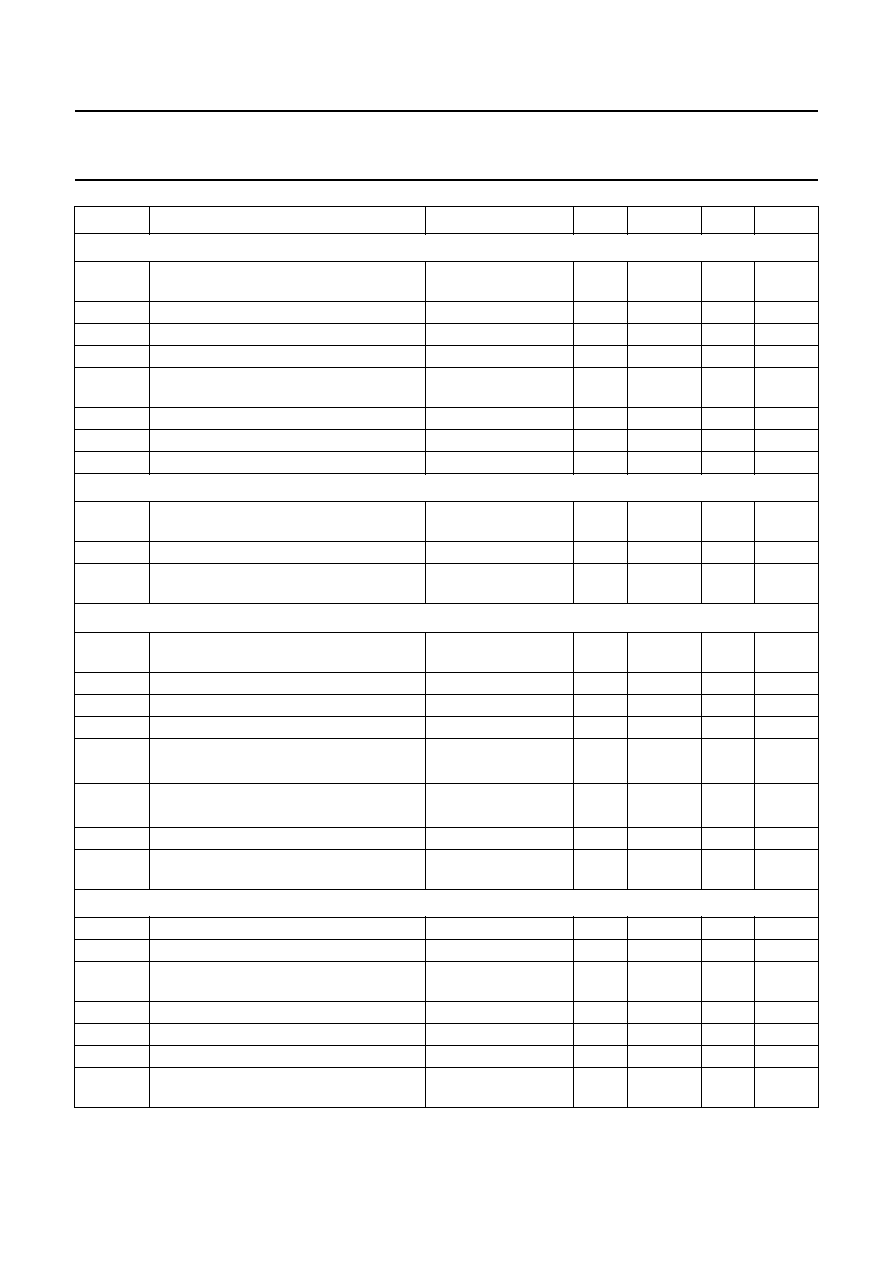
LIMITING VALUES
Limiting values in accordance with the Absolute Maximum System (IEC 134).
Note
1. Equivalent to discharging a 200 pF capacitor through a 0
series resistor.
THERMAL RESISTANCE
SYMBOL
PARAMETER
MIN.
MAX.
UNIT
V
P1
supply voltage 1 (pin 12)
0
6
V
V
P2
supply voltage 2 (pin 47)
0
6
V
V
P3
supply voltage 3 (pin 30)
0
6
V
V
n
voltage on all pins except ground pins
0
V
P
V
P
tot
total power dissipation
0
360
mW
T
stg
storage temperature range
-
25
+
150
∞
C
T
amb
operating ambient temperature range
0
+
70
∞
C
V
ESD
electrostatic handling
(1)
for all pins
±
400
-
V
SYMBOL
PARAMETER
MIN.
MAX.
UNIT
R
th j-a
from junction to ambient in free air
-
92
K/W

September 1990
10
Philips Semiconductors
Preliminary specification
Video signal processor for CD-video/laser vision
TEA7650H
CHARACTERISTICS
V
P1
= V
P2
= V
P3
= 5 V, T
amb
= 25
∞
C, measurements taken in Fig.1-2 ; unless otherwise specified.
Voltages referred to
GND1 (pin 19):
V
P1
and voltage at pins 6 to 15, 18
GND2 (pin 43):
V
P2
and voltage at pins 1 to 4, 16, 37, 44 to 48
GND3 (pin 28):
V
P3
and voltage at pins 5, 17, 20 to 36, 38 to 42
SYMBOL
PARAMETER
CONDITIONS
MIN.
TYP.
MAX.
UNIT
V
P1
supply voltage 1 (pin 12)
4.5
5
5.5
V
V
P2
supply voltage 2 (pin 47)
4.5
5
5.5
V
V
P3
supply voltage 3 (pin 30)
4.5
5
5.5
V
I
12
+
30
+
47
total supply current
-
-
65
mA
Standard select input (pin 37)
V
IL
input voltage for standard PAL (LOW)
0
-
1
V
V
IH
input voltage for standard NTSC (HIGH),
alternative measure for standard NTSC
pin connected
3
-
V
P2
V
pin open-circuit
-
-
-
I
IL
input current (LOW)
V
37
= 1 V
-
-
-
100
µ
A
I
IH
input current (HIGH)
V
37
= 4 V
-
-
20
µ
A
Modulation transfer function MTF (referred to GND1, pin 19)
V
i (p-p)
FM input signal at pin 7
(peak-to-peak value)
50
-
300
mV
for proper MTF correction
50
-
200
mV
Z
7
input impedance
-
5
-
k
MTF control signal
I
(p-p)
output current for storage of the burst
amplitude at pin 5 (peak-to-peak value)
-
200
-
µ
A
I
6
burst amplitude integrator,
charging current (pin 6)
-
±
50
-
µ
A
g
conductance g = dI
6
/ dV
5
-
-
1
-
mS
MTF frequency selection (pins 8 and 9)
pin 8 active for PAL;
pin 9 active for NTSC
V
o (p-p)
output signal
-
V
7 (p-p)
-
mV
Z
output impedance
-
-
10
I
o (p-p)
output current
-
-
4.5
mA
V
o (p-p)
MTF output signal (pin 10)
-
-
300
mV
Z
10
MTF output impedance
-
-
100
G
v
signal gain
G
v
= V
10
/ V
7
G
o
G
v
= G
o
+
20 log G
r
(V
6
)
-
0
-
dB
G
r
minimum gain
V
6
= 0
-
0
-
dB
maximum gain
V
6
= 2.6 V
-
300
/R8
-
maximum gain
V
6
= 2.6 V
-
300
/R9
-
B
bandwidth
-
3 dB; G
r
= 0
15
-
-
MHz
2H
second harmonic suppression
f = 8 MHz
40
-
-
dB
September 1990
11
Philips Semiconductors
Preliminary specification
Video signal processor for CD-video/laser vision
TEA7650H
MTF following amplifier (pins 11 and 13)
V
i (p-p)
FM input signal at pin 11
(peak-to-peak value)
-
-
300
mV
Z
11
input impedance
10
-
-
k
R
E
internal emitter resistor to ground
-
1.8
-
k
Z
13
output impedance (pin 13)
-
-
50
I
o (p-p)
output current at pin 13
(peak-to-peak value)
-
-
1
mA
G
v
voltage gain (pins 13-11)
-
8
-
dB
B
bandwidth (pin 13)
-
3 dB
15
-
-
MHz
2H
second harmonic suppression
40
-
-
dB
Limiting amplifier for demodulator
V
i (p-p)
input signal for proper demodulation
at pin 14 (peak-to-peak value)
0.1
-
1
V
Z
14
input impedance
10
-
-
k
I
(p-p)
charging current of 2nd harmonic control
at pin 15 (peak-to-peak value)
-
200
-
µ
A
FM demodulator with pulswidth-modulated current output (f = 2 f
in
). Referred to GND1, pin 19
I
(p-p)
output current pulse at pin 18
(peak-to-peak value)
-
-
3.2
-
mA
I
18
mean (average) DC current
for top sync
-
-
1.75
-
mA
Z
18
output impedance
30
-
-
k
V
18
DC output voltage range
0
-
2
V
S
transconductance
at PAL
-
-
210
-
µ
A/MHz
at NTSC
-
-
185
-
µ
A/MHz
N
static non-linearity
-
-
10
%
B
bandwidth
±
1 dB
5
-
-
MHz
main carrier suppression
V
14 (p-p)
= 100 mV
35
-
-
dB
I
(p-p)
charging current at pin 16 (amplitude
storage for top sync, peak-to-peak value)
-
26
-
µ
A
De-emphasis amplifier (output pin 21 only for NTSC active). Referred to GND3, pin 28
Z
23
input impedance (pin 23)
10
-
-
k
I
23
DC input current
-
-
2
µ
A
I
(p-p)
charging current for black clamping
capacitor at pin 22 (peak-to-peak value)
-
3
-
µ
A
R
20, 21
output impedance (pins 20 and 21)
-
-
100
V
20, 21
DC output voltage (black level)
-
2.2
-
V
BW
g
gain bandwidth product
40
-
-
MHz
I
24 (p-p)
charging current for AGC capacitor
at pin 24 (peak-to-peak current)
-
11
-
µ
A
SYMBOL
PARAMETER
CONDITIONS
MIN.
TYP.
MAX.
UNIT

September 1990
12
Philips Semiconductors
Preliminary specification
Video signal processor for CD-video/laser vision
TEA7650H
Composite sync output CS1 (pin 2; referred to GND2, pin 43)
V
oH
sync output voltage (active HIGH)
I
2
=
-
0.5 mA
4
-
-
V
V
oL
sync output voltage (LOW)
I
2
= 0.5 mA
-
-
0.4
V
t
d
delay of positive going sync edge
-
-
300
ns
t
d
jitter of positive going sync edge
-
-
40
ns
t
r
, t
f
rise and fall time
C
L
= 22 pF
-
-
200
ns
Vertical sync output (VS), open collector output with 500
internal series resistor, referred to GND2, pin 43
V
4
sync output voltage active LOW (pin 4)
I
4
=
-
0.5 mA
-
-
0,7
V
t
d
delay time
-
18
-
µ
s
t
e
elongation time
-
70
-
µ
s
Drop out processing. (referred to GND3, pin 28)
f
i
frequency range for no drop out
recognition
f
1
minimum value at PAL
-
5.6
-
MHz
f
2
maximum value at PAL
-
9.7
-
MHz
f
1
minimum value at NTSC
-
6.97
-
MHz
f
2
maximum value at NTSC
-
11.1
-
MHz
t
d
delay time on negative going edge
for an abrupt drop out with
f < 0.5 f
1
or f > 1.5 f
2
-
-
250
ns
t
e
drop out elongation time
C3 = 47 pF;
R3 = 100 k
-
3.5
-
µ
s
V
3
output voltage during drop out
internal R
S
= 500
;
I
3
=
-
0.5 mA
-
-
0.7
V
V
3 thr
threshold voltage of drop out switch
-
2
-
V
V
3 DO
input voltage for forced drop out switching
0
0.7
V
V
i (p-p)
delayed video input signal at pin 27
(peak-to-peak value)
R
G
1 k
-
700
-
mV
V
27
DC input voltage (black level)
-
2.2
-
V
Z
27
input impedance
10
-
-
k
I
(p-p)
charging current for coupling capacitor
at pin 27 (peak-to-peak value)
-
3
-
µ
A
I
(p-p)
charging current for AGC of the delayed
signal at pin 26 (peak-to-peak value)
-
11
-
µ
A
SYMBOL
PARAMETER
CONDITIONS
MIN.
TYP.
MAX.
UNIT

September 1990
13
Philips Semiconductors
Preliminary specification
Video signal processor for CD-video/laser vision
TEA7650H
Chrominance output for purpose of ETBC, with R
L
= 5 k
(pin 48) and nominal input signal. Resonant circuit at pin
1 tuned to 4.43 MHz for PAL (3.58 MHz for NTSC). Referred to GND2, pin 43. See previous comment to
characteristics.
V
o (p-p)
burst amplitude (peak-to-peak value)
at pin 48
PAL; f = 4.43 MHz
-
760
-
mV
NTSC; f = 3.58 MHz
-
725
-
mV
Z
48
output impedance
-
-
250
I
o (p-p)
output current (peak-to-peak value)
-
-
700
µ
A
CR
crosstalk attenuation from pin 44
32
-
-
dB
R
1
output impedance for resonant circuit
-
1.4
-
k
Electronic time base control ETBC and CCD delay (external). Referred to GND3, pin 28.
V
o (p-p)
CVBS output signal of emitter output
at pin 29 (peak-to-peak value)
V
20 (p-p)
= 0.5 V
±
3 dB
(peak-to-peak value)
-
850
-
mV
burst amplitude in signal
for PAL
-
230
-
mV
for NTSC
-
219
-
mV
V
29
DC output voltage (black level)
-
1.85
-
V
Z
29
output impedance
-
-
V
t
/ I
29
-
I
29
output current (source)
-
-
-
3
mA
S/N
signal-to-noise ratio from pin 7 to pin 29
5 MHz unweighted
50
-
-
dB
V
o (p-p)
difference of CVBS amplitude
(peak-to-peak value)
switching from main
to delayed signal;
V
27 (p-p)
= 0.7 V
at pin 29 referred to 0 dB level
0 dB
-
±
2
%
at pin 29 referred to
±
4 dB level
±
4 dB
-
-
±
6
%
CR
crosstalk attenuation
f = 2 MHz
35
-
-
dB
V
29
offset voltage after switching
-
-
10
mV
V
S
spike amplitude at switching (pin 29)
t
S
> 50 ns
-
-
15
mV
Chrominance and luminance amplifier (referred to GND3, pin 28).
V
i (p-p)
delayed CVBS input signal (pin 31)
R
G
1 k
-
600
-
mV
V
31
DC input voltage (black level)
-
2.2
-
V
Z
31
input impedance
10
-
-
k
I
(p-p)
charging current for coupling capacitor
at pin 31 (peak-to-peak value)
-
3
-
µ
A
I
(p-p)
charging current for AGC
at pin 32 (peak-to-peak value)
-
11
-
µ
A
SYMBOL
PARAMETER
CONDITIONS
MIN.
TYP.
MAX.
UNIT

September 1990
14
Philips Semiconductors
Preliminary specification
Video signal processor for CD-video/laser vision
TEA7650H
Chrominance output for purpose of ETBC, with R
L
= 5 k
(pin 44) and nominal input signal. Resonant circuit at pin
45 tuned to 4.43 MHz for PAL (3.58 MHz for NTSC). Referred to GND2, pin 43. See previous comment to
characteristics.
V
o (p-p)
burst amplitude (peak-to-peak value)
at pins 44
for PAL
f = 4.43 MHz
-
760
-
mV
for NTSC
f = 3.58 MHz
-
725
-
mV
Z
44
output impedance
-
-
250
I
o (p-p)
output current (peak-to-peak value)
-
-
700
µ
A
CR
crosstalk attenuation from pin 48
32
-
-
dB
R
45
output impedance for resonant circuit
-
1.4
-
k
Luminance noise reduction (referred to GND3, pin 28)
V
(p-p)
output signal at pin 33
(peak-to-peak value)
V
i (p-p)
= 0.6 V
±
3 dB
at pin 31
-
1
-
V
V
33
DC output voltage (black level)
-
2.2
-
V
I
E
internal emitter current to ground
of emitter follower
-
1
-
mA
Z
33
output impedance
-
-
100
I
o (p-p)
AC output current at pin 33
(peak-to-peak value)
-
-
1.5
mA
I
(p-p)
chroma trap switch, active for NTSC
input current (peak-to-peak value)
-
-
350
µ
A
Z
34
input impedance (pin 34)
-
-
50
V
i (p-p)
limiter amplifier input signal at pin 35
(peak-to-peak value)
-
1
-
V
input signal for start of limiting
0
-
100
mV
Z
35
input impedance
-
2
-
k
V
36
voltage range or limiter control (pin 36)
0.1
-
1.5
V
voltage for control-off
-
0
-
V
I
36
DC output current
-
-
100
-
µ
A
Main CVBS output (referred to GND3, pin 28).
V
o (p-p)
CVBS output signal of emitter output
at pin 42 (peak-to-peak value)
V
i (p-p)
= 0.6 V
±
0 dB
at pin 31
-
1
-
V
V
o (p-p)
residual variation of output voltage
at pin 42 (peak-to-peak value)
V
i (p-p)
= 0.6 V
±
3 dB
at pin 31
-
-
±
3
%
V
42
DC output voltage (black level)
-
2.2
-
V
I
E
internal emitter current to ground
of emitter follower
-
300
-
µ
A
Z
42
output impedance
-
-
100
I
o
output source current
-
-
-
5
mA
B
video bandwidth
-
3 dB
5
MHz
S/N
signal-to-noise ratio from pin 31 to pin 42
5 MHz unweighted
60
-
-
dB
SYMBOL
PARAMETER
CONDITIONS
MIN.
TYP.
MAX.
UNIT

September 1990
15
Philips Semiconductors
Preliminary specification
Video signal processor for CD-video/laser vision
TEA7650H
CR
crosstalk attenuation between main
and inserted signal
f = 5 MHz
45
-
-
dB
differences at output due to switching
from main to inserted signal (pin 42)
burst
suppression of special burst
35
-
-
dB
V
42
offset voltage after switching
-
-
50
mV
V
S
spike amplitude at switching
t
S
> 50 ns
-
-
20
mV
V
VID
video attenuation for internal signal
V
39
= HIGH
-
6
-
dB
External video insertion input and switching control
V
i (p-p)
input signal at pin 40 (peak-to-peak value) R
G
1 k
-
1
-
V
V
40
DC voltage (black level)
-
2.9
-
V
G
v
voltage gain (pins 42-40)
-
0
-
dB
Z
40
input impedance
10
-
-
k
I
(p-p)
charging current at pin 40
(peak-to-peak value)
-
3
-
µ
A
B
video bandwidth
-
3 dB
8
-
-
MHz
V
38
voltage for insertion-on (HIGH)
3
-
V
P
V
voltage for insertion-off (LOW)
0
-
1
V
I
38
input current (HIGH)
V
38
= 4 V
-
-
2
µ
A
input current (LOW)
V
38
= 1 V
-
-
-
10
µ
A
t
d
switchover delay time
-
-
50
ns
V
39
voltage for video attenuation-on (HIGH)
-
6 dB video
3
-
V
P
V
voltage for video attenuation-off (LOW)
0 dB video
0
-
1
V
I
39
input current (HIGH)
V
39
= 4 V
-
-
2
µ
A
I
39
input current (LOW)
V
39
= 1 V
-
-
-
10
µ
A
t
d
switchover delay time
-
-
100
ns
Data output and data request input (pins 25 and 17)
V
25
output voltage HIGH-level (pin 25)
I
25
=
-
0.5 mA
3.5
-
-
V
output voltage LOW-level
I
25
= 0.5 mA
-
-
0.8
V
t
p
duty factor (t
p
/ T)
-
50
-
%
t
r
and t
f
rise and fall time
C
L
= 22 pF
-
-
150
ns
t
d
delay time
-
-
200
ns
V
17
voltage for data request-on (HIGH)
at pin 17
3
-
V
P
V
voltage for data request-off (LOW)
0
-
1
V
I
17
input current (HIGH)
V
17
= 4 V
-
-
20
µ
A
input current (LOW)
V
17
= 1 V
-
-
-
100
µ
A
t
d
data delay time
-
-
200
ns
SYMBOL
PARAMETER
CONDITIONS
MIN.
TYP.
MAX.
UNIT

September 1990
16
Philips Semiconductors
Preliminary specification
Video signal processor for CD-video/laser vision
TEA7650H
Composite sync output CS2 (referred to GND2, pin 43)
V
46
sync output voltage (active HIGH)
I
46
=
-
0.5 mA
4
-
-
V
sync output voltage at pin 46 (LOW)
I
46
= 0.5 mA
-
-
0.4
V
t
d
delay of positive going sync edge
-
-
300
ns
t
d
jitter of positive going sync edge
-
-
40
ns
t
r
rise time
C
L 46
= 22 pF
-
-
150
ns
t
f
fall time
C
L 46
= 22 pF
-
-
200
ns
Reference output voltage (referred to GND3, pin 28)
V
ref
reference output voltage (pin 41)
-
1.6
-
V
R
41
output resistance
-
-
5
k
I
ref
output current (used for CCD reference)
-
-
±
10
µ
A
dV
41
/dV
P
supply voltage dependence
-
-
-
20
dB
dV
41
dependence of junction temperature
T
j
= 20 to 120
∞
C
-
-
±
30
mV
SYMBOL
PARAMETER
CONDITIONS
MIN.
TYP.
MAX.
UNIT

September 1990
17
Philips Semiconductors
Preliminary specification
Video signal processor for CD-video/laser vision
TEA7650H
APPLICATION INFORMATION
Fig.4 Internal circuits; (continued in Fig.5).

September 1990
18
Philips Semiconductors
Preliminary specification
Video signal processor for CD-video/laser vision
TEA7650H
Fig.5 Internal circuits; (continued from Fig.4).

September 1990
19
Philips Semiconductors
Preliminary specification
Video signal processor for CD-video/laser vision
TEA7650H
Fig.6 Internal circuits; (continued from Fig.5).

September 1990
20
Philips Semiconductors
Preliminary specification
Video signal processor for CD-video/laser vision
TEA7650H
Fig.7 Internal circuits; (continued from Fig.6).

September 1990
21
Philips Semiconductors
Preliminary specification
Video signal processor for CD-video/laser vision
TEA7650H
PACKAGE OUTLINE
UNIT
A
1
A
2
A
3
b
p
c
E
(1)
e
H
E
L
L
p
Q
Z
y
w
v
REFERENCES
OUTLINE
VERSION
EUROPEAN
PROJECTION
ISSUE DATE
IEC
JEDEC
EIAJ
mm
0.3
0.1
1.85
1.65
0.25
0.42
0.28
0.25
0.14
10.1
9.9
0.75
15.5
14.5
1.05
0.75
1.05
0.70
7
0
o
o
0.15
0.1
0.3
2.5
DIMENSIONS (mm are the original dimensions)
Note
1. Plastic or metal protrusions of 0.25 mm maximum per side are not included.
2.4
1.6
SOT196-1
92-11-17
95-02-04
D
(1)
(1)
(1)
10.1
9.9
H
D
15.5
14.5
E
Z
1.05
0.70
D
b
p
e
E
A
1
A
L
p
Q
detail X
L
(A )
3
B
12
c
D
H
b
p
E
H
A
2
v
M
B
D
Z D
A
Z E
e
v
M
A
X
1
48
37
36
25
24
13
y
pin 1 index
w
M
w
M
0
2.5
5 mm
scale
QFP48: plastic quad flat package; 48 leads (lead length 2.5 mm); body 10 x 10 x 1.75 mm
SOT196-1
A
max.
2.20

September 1990
22
Philips Semiconductors
Preliminary specification
Video signal processor for CD-video/laser vision
TEA7650H
SOLDERING
Introduction
There is no soldering method that is ideal for all IC
packages. Wave soldering is often preferred when
through-hole and surface mounted components are mixed
on one printed-circuit board. However, wave soldering is
not always suitable for surface mounted ICs, or for
printed-circuits with high population densities. In these
situations reflow soldering is often used.
This text gives a very brief insight to a complex technology.
A more in-depth account of soldering ICs can be found in
our
"IC Package Databook" (order code 9398 652 90011).
Reflow soldering
Reflow soldering techniques are suitable for all QFP
packages.
The choice of heating method may be influenced by larger
plastic QFP packages (44 leads, or more). If infrared or
vapour phase heating is used and the large packages are
not absolutely dry (less than 0.1% moisture content by
weight), vaporization of the small amount of moisture in
them can cause cracking of the plastic body. For more
information, refer to the Drypack chapter in our
"Quality
Reference Handbook" (order code 9397 750 00192).
Reflow soldering requires solder paste (a suspension of
fine solder particles, flux and binding agent) to be applied
to the printed-circuit board by screen printing, stencilling or
pressure-syringe dispensing before package placement.
Several techniques exist for reflowing; for example,
thermal conduction by heated belt. Dwell times vary
between 50 and 300 seconds depending on heating
method. Typical reflow temperatures range from
215 to 250
∞
C.
Preheating is necessary to dry the paste and evaporate
the binding agent. Preheating duration: 45 minutes at
45
∞
C.
Wave soldering
Wave soldering is not recommended for QFP packages.
This is because of the likelihood of solder bridging due to
closely-spaced leads and the possibility of incomplete
solder penetration in multi-lead devices.
If wave soldering cannot be avoided, the following
conditions must be observed:
∑
A double-wave (a turbulent wave with high upward
pressure followed by a smooth laminar wave)
soldering technique should be used.
∑
The footprint must be at an angle of 45
∞
to the board
direction and must incorporate solder thieves
downstream and at the side corners.
Even with these conditions, do not consider wave
soldering the following packages: QFP52 (SOT379-1),
QFP100 (SOT317-1), QFP100 (SOT317-2),
QFP100 (SOT382-1) or QFP160 (SOT322-1).
During placement and before soldering, the package must
be fixed with a droplet of adhesive. The adhesive can be
applied by screen printing, pin transfer or syringe
dispensing. The package can be soldered after the
adhesive is cured.
Maximum permissible solder temperature is 260
∞
C, and
maximum duration of package immersion in solder is
10 seconds, if cooled to less than 150
∞
C within
6 seconds. Typical dwell time is 4 seconds at 250
∞
C.
A mildly-activated flux will eliminate the need for removal
of corrosive residues in most applications.
Repairing soldered joints
Fix the component by first soldering two diagonally-
opposite end leads. Use only a low voltage soldering iron
(less than 24 V) applied to the flat part of the lead. Contact
time must be limited to 10 seconds at up to 300
∞
C. When
using a dedicated tool, all other leads can be soldered in
one operation within 2 to 5 seconds between
270 and 320
∞
C.

September 1990
23
Philips Semiconductors
Preliminary specification
Video signal processor for CD-video/laser
vision
TEA7650H
DEFINITIONS
LIFE SUPPORT APPLICATIONS
These products are not designed for use in life support appliances, devices, or systems where malfunction of these
products can reasonably be expected to result in personal injury. Philips customers using or selling these products for
use in such applications do so at their own risk and agree to fully indemnify Philips for any damages resulting from such
improper use or sale.
Data sheet status
Objective specification
This data sheet contains target or goal specifications for product development.
Preliminary specification
This data sheet contains preliminary data; supplementary data may be published later.
Product specification
This data sheet contains final product specifications.
Limiting values
Limiting values given are in accordance with the Absolute Maximum Rating System (IEC 134). Stress above one or
more of the limiting values may cause permanent damage to the device. These are stress ratings only and operation
of the device at these or at any other conditions above those given in the Characteristics sections of the specification
is not implied. Exposure to limiting values for extended periods may affect device reliability.
Application information
Where application information is given, it is advisory and does not form part of the specification.