Document Outline
- FEATURES
- APPLICATIONS
- GENERAL DESCRIPTION
- ORDERING INFORMATION
- BLOCK DIAGRAM
- PINNING
- FUNCTIONAL DESCRIPTION
- AGC
- LIMITING VALUES
- HANDLING
- THERMAL CHARACTERISTICS
- CHARACTERISTICS
- TYPICAL PERFORMANCE CHARACTERISTICS
- APPLICATION INFORMATION
- BONDING PAD LOCATIONS
- PACKAGE OUTLINE
- SOLDERING
- DATA SHEET STATUS
- DEFINITIONS
- DISCLAIMERS

DATA SHEET
Product specification
Supersedes data of 2000 Sep 29
2002 Sep 06
INTEGRATED CIRCUITS
TZA3033
SDH/SONET STM1/OC3
transimpedance amplifier

2002 Sep 06
2
Philips Semiconductors
Product specification
SDH/SONET STM1/OC3
transimpedance amplifier
TZA3033
FEATURES
∑
Low equivalent input noise of 1 pA/
Hz (typical)
∑
Wide dynamic range from 0.25
µ
A to 1.6 mA (typical)
∑
Differential transimpedance of 44 k
∑
Bandwidth typical 130 MHz
∑
Differential outputs
∑
On-chip Automatic Gain Control (AGC)
∑
No external components required
∑
Single supply voltage from 3.0 to 5.5 V
∑
Bias voltage for PIN diode
∑
Pin compatible with SA5223
∑
Goldplated version available for direct placement of
photodiode on die.
APPLICATIONS
∑
Digital fibre optic receiver in short, medium and long
haul optical telecommunications transmission systems
or in high speed data networks
∑
Wideband RF gain block.
GENERAL DESCRIPTION
The TZA3033 is a low-noise transimpedance amplifier with
AGC designed to be used in STM1/OC3 fibre optic links.
It amplifies the current generated by a photo detector
(PIN diode or avalanche photodiode) and converts it to a
differential output voltage.
ORDERING INFORMATION
TYPE
NUMBER
PACKAGE
NAME
DESCRIPTION
VERSION
TZA3033T
SO8
plastic small outline package; 8 leads; body width 3.9 mm
SOT96-1
TZA3033U
-
bare die in waffle pack carriers; die dimensions 1.030
◊
1.300 mm
-
TZA3033U/G
-
bare die with goldplating in waffle pack carriers; die dimensions
1.030
◊
1.300 mm
-
2002 Sep 06
3
Philips Semiconductors
Product specification
SDH/SONET STM1/OC3
transimpedance amplifier
TZA3033
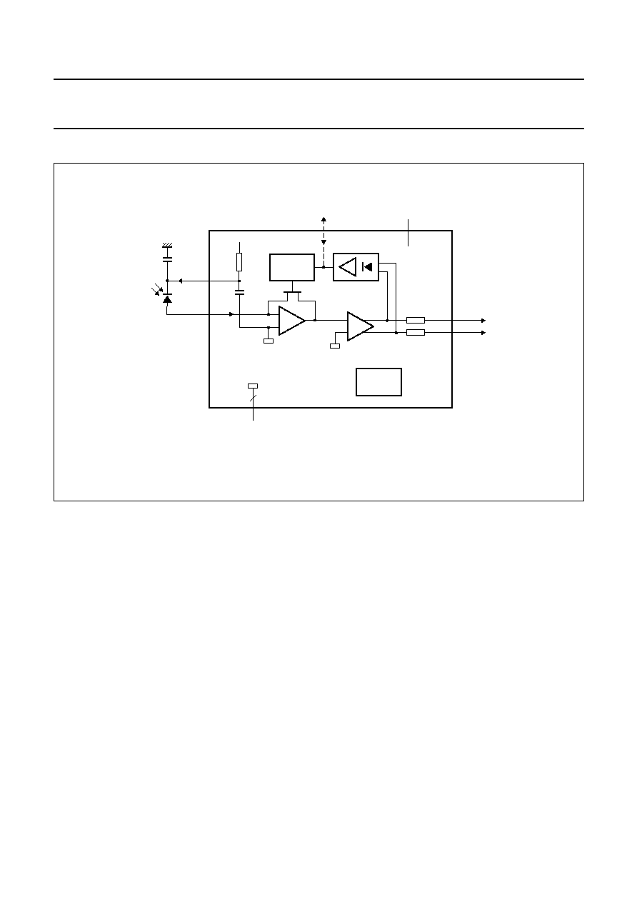
BLOCK DIAGRAM
handbook, full pagewidth
GAIN
CONTROL
BIASING
A2
A1
1 (1)
1 nF
DREF
3 (5)
IPhoto
low noise
amplifier
single-ended to
differential converter
VCC
8 (13, 14)
(15)
VCC
3
2, 4, 5 (3, 4, 7, 8, 9, 10)
GND
AGC
(1)
peak detector
TZA3033
(11) 6
OUT
(12) 7
OUTQ
MGR368
65 pF
250
Fig.1 Block diagram.
The numbers in brackets refer to the pad numbers of the bare die version.
(1) AGC analog I/O is only available on the TZA3033U (pad 15).

2002 Sep 06
4
Philips Semiconductors
Product specification
SDH/SONET STM1/OC3
transimpedance amplifier
TZA3033
PINNING
Note
1. For the TZA3033U/G this pad is connected to the gold layer on top of the passivation layer.
SYMBOL
PIN
TZA3033T
PAD
TZA3033U
TYPE
DESCRIPTION
DREF
1
1
analog output
bias voltage for PIN diode; cathode should be connected to
this pin; note 1
TESTA
-
2
-
for test purposes only; to be left open in application
GND
2
3, 4
ground
ground
IPhoto
3
5
analog input
current input; anode of PIN diode should be connected to this
pin; DC bias voltage is 1048 mV
TESTB
-
6
-
for test purposes only; to be left open in application
GND
4
7, 8
ground
ground
GND
5
9, 10
ground
ground
OUT
6
11
output
data output; pin OUT goes HIGH when current flows into
pin IPhoto
OUTQ
7
12
output
data output; compliment of pin OUT
V
CC
8
13, 14
supply
supply voltage
AGC
-
15
input/output
AGC analog I/O
handbook, halfpage
1
2
3
4
8
7
6
5
MGR369
TZA3033T
VCC
OUTQ
GND
OUT
GND
GND
IPhoto
DREF
Fig.2 Pin configuration.
2002 Sep 06
5
Philips Semiconductors
Product specification
SDH/SONET STM1/OC3
transimpedance amplifier
TZA3033
FUNCTIONAL DESCRIPTION
The TZA3033 is a transimpedance amplifier intended for
use in fibre optic links for signal recovery in STM1/OC3
applications. It amplifies the current generated by a photo
detector (PIN diode or avalanche photodiode) and
transforms it into a differential output voltage. The most
important characteristics of the TZA3033 are high receiver
sensitivity and wide dynamic range.
High receiver sensitivity is achieved by minimizing noise in
the transimpedance amplifier. The signal current
generated by a PIN diode can vary between
0.25
µ
A to 1.6 mA (p-p). An AGC loop (see Fig.1) is
implemented to make it possible to handle such a wide
dynamic range. The AGC loop increases the dynamic
range of the receiver by reducing the feedback resistance
of the preamplifier.
The AGC loop hold capacitor is integrated on-chip, so an
external capacitor is not needed for AGC. The AGC
voltage can be monitored at pad 15 on the bare die
(TZA3033U). Pad 15 is not bonded in the packaged device
(TZA3033T). This pad can be left unconnected during
normal operation. It can also be used to force an external
AGC voltage. If pad 15 (AGC) is connected to V
CC
, the
internal AGC loop is disabled and the receiver gain is at a
maximum. The maximum input current is then
approximately 10
µ
A.
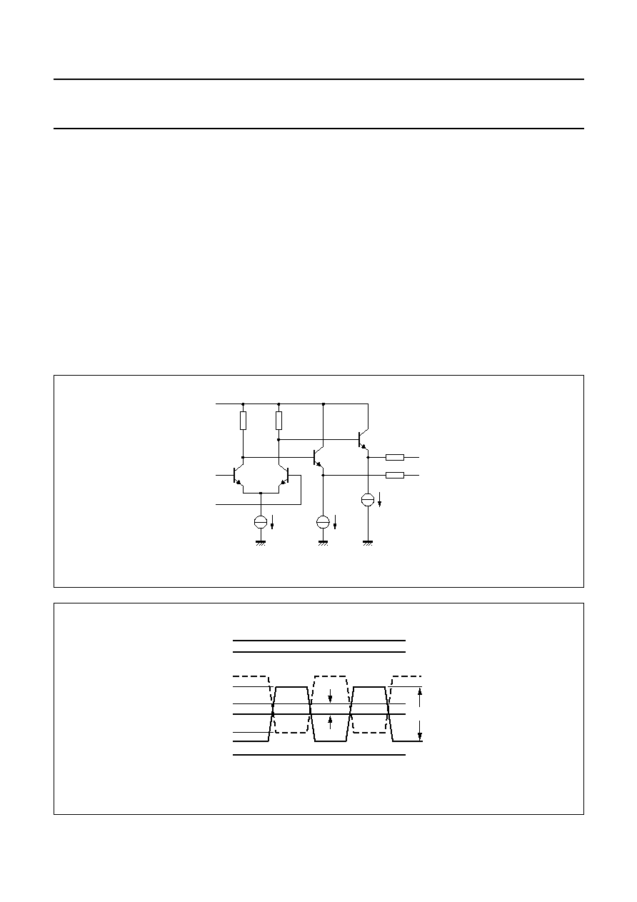
A differential amplifier converts the output of the
preamplifier to a differential voltage (see Fig.3).
The logic level symbol definitions are shown in Fig.4.
handbook, full pagewidth
MGT547
266
266
30
VCC
OUTQ
OUT
4.5 mA
2 mA
4.5 mA
30
Fig.3 Data output circuit.
handbook, full pagewidth
MGR243
VOO
VO(max)
VOQH
VOH
VOQL
VOL
VO(min)
Vo(p-p)
VCC
Fig.4 Logic level symbol definitions for data outputs OUT and OUTQ.
2002 Sep 06
6
Philips Semiconductors
Product specification
SDH/SONET STM1/OC3
transimpedance amplifier
TZA3033
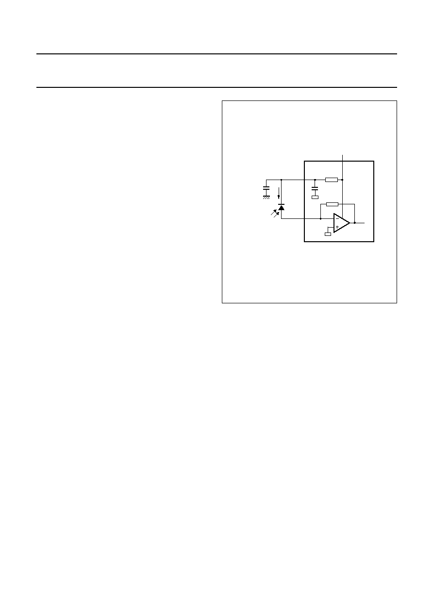
PIN diode bias voltage DREF
The transimpedance amplifier together with the PIN diode
determine to a large extent the performance of an optical
receiver. The key parameters of a transimpedance
amplifier like sensitivity, bandwidth, and the Power Supply
Rejection Ratio (PSSR), are especially influenced by how
the PIN diode is connected to the input and the layout
around the input pin. The total capacitance at the input pin
is critical to obtain the highest sensitivity. It should be kept
to a minimum by reducing the capacitor of the PIN diode
and the parasitics around the input pin. The PIN diode
should be placed very close to the IC to reduce the
parasitics. Because the capacitance of the PIN diode
depends on the reverse voltage across it, the reverse
voltage should be selected as high as possible.
The PIN diode can be connected to the input as shown in
Fig.5. In Fig.5 the PIN diode is connected between DREF
and IPhoto. Pin DREF provides an easy bias voltage for
the PIN diode. The voltage at DREF is derived from V
CC
by
a low-pass filter. The low-pass filter consisting of the
internal resistor R1, the internal capacitor C1 and the
external capacitor C2 rejects the supply voltage noise. The
external capacitor C2 should be equal to or larger than
1 nF for a high PSRR.
It is preferable to connect the cathode of the PIN diode to
a voltage higher than V
CC
when such a voltage source is
available on the board. In this case the DREF pin can be
left unconnected.
The reverse voltage across the PIN diode is 3.95 V
(5
-
1.05 V) for a 5 V supply and 2.25 V (3.3
-
1.05 V) for
a 3.3 V supply.
MGT548
R1
250
C1
65 pF
C2
1 nF
VCC
Ii
1
8
TZA3033
3
IPhoto
DREF
Fig.5 Connecting the PIN diode to the input.
2002 Sep 06
7
Philips Semiconductors
Product specification
SDH/SONET STM1/OC3
transimpedance amplifier
TZA3033
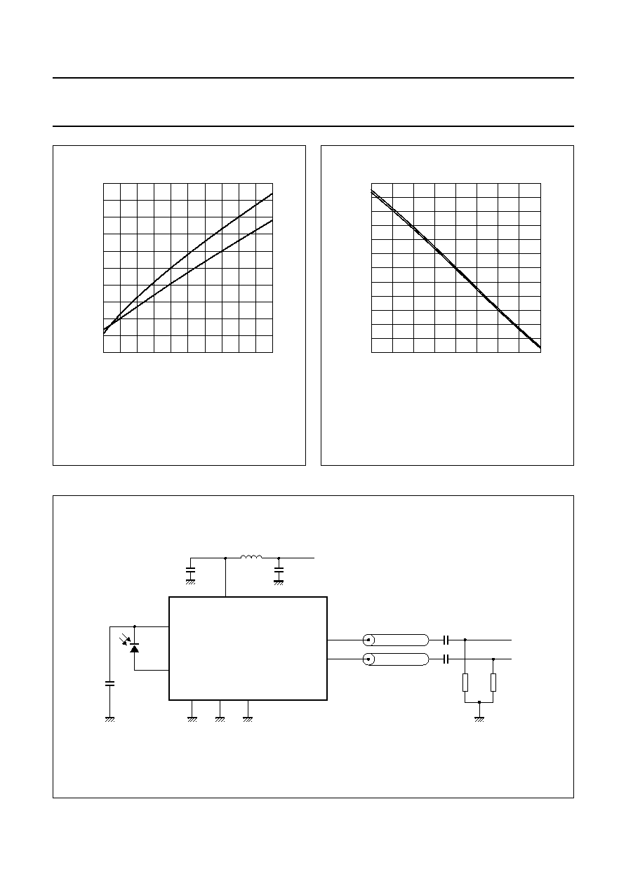
AGC
The TZA3033 transimpedance amplifier can handle input
currents from 0.25
µ
A to 1.6 mA. This means a dynamic
range of 79 dB. At low input currents, the transimpedance
must be high to obtain an adequate output voltage, and the
noise should be suitably low to guarantee minimum bit
error rate. At high input currents however, the
transimpedance should be low to avoid pulse width
distortion. This means that the gain of the amplifier has to
vary depending on the input signal level to handle such a
wide dynamic range. This is achieved in the TZA3033 by
implementing an Automatic Gain Control (AGC) loop.
The AGC loop consists of a peak detector, a hold capacitor
and a gain control circuit. The peak amplitude of the signal
is detected by the peak detector and stored on the hold
capacitor. The voltage across the hold capacitor is
compared to a threshold level. The threshold level is set at
an input current of 2.5
µ
A (p-p). AGC becomes active only
for input signals larger than the threshold level. It is
disabled for smaller signals. The transimpedance is then
at its maximum value (44 k
differential).
When the AGC is active, the feedback resistance of the
transimpedance amplifier is reduced to keep the output
voltage constant. The transimpedance is regulated from
44 k
at low currents (I < 2.5
µ
A) to 200
at high currents
(I < 500
µ
A). Above 500
µ
A the transimpedance is at its
minimum and can not be reduced further but the front-end
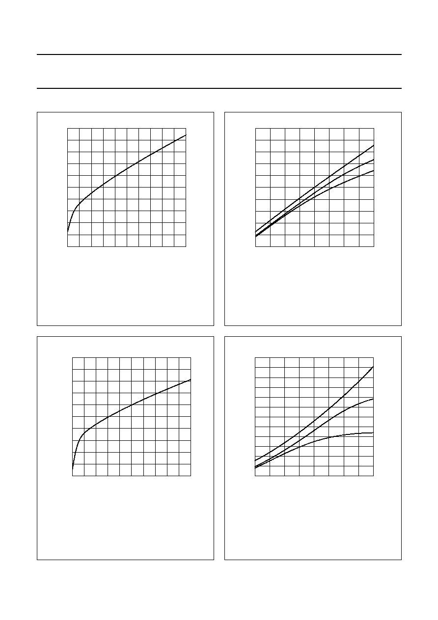
remains linear until input currents of 1.6 mA (p-p).
The upper graph of Fig.6 shows the output voltages V
OUT
and V
OUTQ
of the TZA3033 as a function of the DC input
current for a supply voltage of 3 V. In the lower graph the
difference between both output voltages, V
o(dif)
, is shown
for supply voltages of 3, 3.3 and 5 V. It can seen from the
graph that the output changes linearly up to an input
current of 2.5
µ
A where the AGC becomes active. From
this point on, the AGC tries to keep the differential output
voltage constant around 110 mV for medium range input
currents (input currents < 200
µ
A). The AGC can not
regulate for input currents above 500
µ
A, and the output
voltage rises again with the input current.
handbook, full pagewidth
2.05
300
0
10
-
1
1
10
10
2
10
3
10
4
MGT562
1.85
1.75
1.65
200
100
1.95
Ii (
µ
A)
Vo
(V)
Vo(dif)
(mV)
(1)
(2)
(3)
VOUT
VCC = 3 V
VOUTQ
Fig.6 AGC characteristics.
(1) V
CC
= 3.0 V.
(2) V
CC
= 3.3 V.
(3) V
CC
= 5.0 V.
2002 Sep 06
8
Philips Semiconductors
Product specification
SDH/SONET STM1/OC3
transimpedance amplifier
TZA3033
LIMITING VALUES
In accordance with the Absolute Maximum Rating System (IEC 60134).
HANDLING
Precautions should be taken to avoid damage through electrostatic discharge. This is particularly important during
assembly and handling of the bare die. Additional safety can be obtained by bonding the V
CC
and GND pads first, the
remaining pads may then be bonded to their external connections in any order.
THERMAL CHARACTERISTICS
SYMBOL
PARAMETER
MIN.
MAX.
UNIT
V
CC
supply voltage
-
0.5
+5.5
V
V
n
DC voltage
pin 3/pad 5: IPhoto
-
0.5
+2
V
pins 6 and 7/pads 11 and 12: OUT and OUTQ
-
0.5
V
CC
+ 0.5
V
pad 15: AGC (TZA3033U only)
-
0.5
V
CC
+ 0.5
V
pin 1/pad 1: DREF
-
0.5
V
CC
+ 0.5
V
I
n
DC current
pin 3/pad 5: IPhoto
-
1
+2.5
mA
pins 6 and 7/pads 11 and 12: OUT and OUTQ
-
15
+15
mA
pad 15: AGC (TZA3033U only)
-
0.2
+0.2
mA
pin 1/pad 1: DREF
-
2.5
+2.5
mA
P
tot
total power dissipation
-
300
mW
T
stg
storage temperature
-
65
+150
∞
C
T
j
junction temperature
-
150
∞
C
T
amb
ambient temperature
-
40
+85
∞
C
SYMBOL
PARAMETER
VALUE
UNIT
R
th(j-s)
thermal resistance from junction to solder point
160
K/W
2002 Sep 06
9
Philips Semiconductors
Product specification
SDH/SONET STM1/OC3
transimpedance amplifier
TZA3033
CHARACTERISTICS
For typical values T
amb
= 25
∞
C and V
CC
= 5 V; minimum and maximum values are valid over the entire ambient
temperature range and process spread; all voltages are measured with respect to ground; unless otherwise specified.
SYMBOL
PARAMETER
CONDITIONS
MIN.
TYP.
MAX.
UNIT
V
CC
supply voltage
3
5
5.5
V
I
CC
supply current
AC coupled; R
L
= 50
V
CC
= 5 V
20
38
60
mA
V
CC
= 3.3 V
20
35
50
mA
P
tot
total power dissipation
V
CC
= 5 V
100
190
330
mW
V
CC
= 3.3 V
60
116
180
mW
T
j
junction temperature
-
40
-
+125
∞
C
T
amb
ambient temperature
-
40
+25
+85
∞
C
R
tr
small-signal transresistance
of the receiver
AC coupled; measured
differentially
R
L
=
42
90
112
k
R
L
= 50
21
45
66
k
f
-
3dB(h)
high frequency
-
3 dB point
AC coupled; measured
differentially; C
i
= 0.7 pF;
R
L
= 50
T
j
= 125
∞
C
90
130
-
MHz
T
j
= 100
∞
C
100
130
-
MHz
PSRR
power supply rejection ratio
measured differentially;
note 1
f = 100 kHz to 10 MHz
-
0.5
-
µ
A/V
f = 100 MHz
-
10
-
µ
A/V
Bias voltage: pin DREF
R
DREF
resistance between pins
DREF and V
CC
DC tested
210
245
290
Input: pin IPhoto
V
bias(IPhoto)
input bias voltage on
pin IPhoto
800
1050
1300
mV
I
i(IPhoto)(p-p)
input current on pin IPhoto
(peak-to-peak value)
note 2
V
CC
= 5 V
0
1
1800
µ
A
V
CC
= 3.3 V
0
1
1600
µ
A
R
i
small-signal input resistance
f
i
= 1 MHz;
input current < 0.5
µ
A
-
330
-
I
n(tot)
total integrated RMS noise
current over bandwidth
(referenced to input)
f = 90 MHz; note 3
-
16
-
nA
2002 Sep 06
10
Philips Semiconductors
Product specification
SDH/SONET STM1/OC3
transimpedance amplifier
TZA3033
Notes
1. PSRR is defined as the ratio of the equivalent current change at the input (
I
IPhoto
) to a change in supply voltage:
For example, a + 4 mV disturbance on V
CC
at 10 MHz will typically add an extra 2 nA to the photodiode current. The
external capacitor between DREF and GND has a large impact on PSRR. The specification is valid with an external
capacitor of 1 nF. The PSSR is guaranteed by design.
2. The Pulse Width Distortion (PWD) is <5% over the whole input current range. The PWD is defined as:
where T is the clock period. The PWD is measured differentially with
PRBS pattern of 10
-
23
.
3. All I
n(tot)
measurements were made with an input capacitance of C
i
= 1 pF. This was comprised of 0.5 pF for the
photodiode itself, with 0.3 pF allowed for the printed-circuit board layout and 0.2 pF intrinsic to the package. Noise
performance is measured differentially.
Data outputs: OUT and OUTQ
V
o(cm)
common mode output voltage AC coupled; R
L
= 50
V
CC
-
1.34
V
CC
-
1.15
V
CC
-
0.96
V
V
o(se)(p-p)
single-ended output voltage
(peak-to-peak value)
AC coupled; R
L
= 50
;
input current = 100
µ
A
(p-p)
40
110
200
mV
V
OO
differential output offset
voltage
V
CC
= 5 V
-
50
+55
+150
mV
V
CC
= 3.3 V
-
50
+35
+100
mV
R
o(se)
single-ended output
resistance
DC tested
36
44
57
t
r
rise time
20% to 80%
-
2.3
3.9
ns
t
f
fall time
80% to 20%
-
2.3
3.9
ns
Automatic gain control loop: pad AGC
I
th(AGC)
AGC threshold current
referred to the peak input
current; tested at 10 MHz
-
2.5
-
µ
A
t
att(AGC)
AGC attack time
-
5
-
µ
s
t
decay(AGC)
AGC decay time
-
10
-
ms
SYMBOL
PARAMETER
CONDITIONS
MIN.
TYP.
MAX.
UNIT
PSRR
I
IPhoto
V
CC
-------------------
=
PWD
pulse width
T
------------------------------
1
≠
100%
◊
=
2002 Sep 06
11
Philips Semiconductors
Product specification
SDH/SONET STM1/OC3
transimpedance amplifier
TZA3033
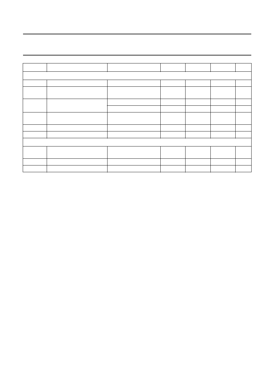
TYPICAL PERFORMANCE CHARACTERISTICS
handbook, halfpage
3.0
5.5
36.5
34.0
34.5
MGT549
35.0
35.5
36.0
ICC
(mA)
3.5
4.0
4.5
5.0
VCC (V)
Fig.7
Supply current as a function of the supply
voltage.
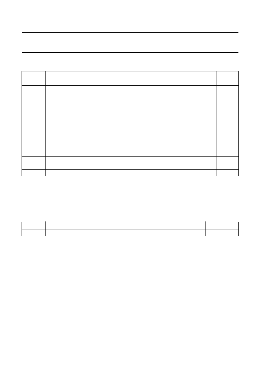
handbook, halfpage
-
40
0
40
120
50
25
40
45
MGT550
80
(3)
(2)
(1)
Tj (
∞
C)
35
30
ICC
(mA)
Fig.8
Supply current as a function of the junction
temperature.
(1) V
CC
= 5 V.
(2) V
CC
= 3.3 V.
(3) V
CC
= 3 V.
handbook, halfpage
3.0
5.5
1.055
1.030
1.035
MGT551
1.040
1.045
1.050
Vi
(V)
3.5
4.0
4.5
5.0
VCC (V)
Fig.9
Input voltage as a function of the supply
voltage.
handbook, halfpage
-
40
0
40
120
1.12
1.00
1.08
1.10
MGT552
80
(3)
(2)
(1)
Tj (
∞
C)
1.06
1.04
1.02
Vi
(V)
Fig.10 Input voltage as a function of the junction
temperature.
(1) V
CC
= 5 V.
(2) V
CC
= 3.3 V.
(3) V
CC
= 3 V.
2002 Sep 06
12
Philips Semiconductors
Product specification
SDH/SONET STM1/OC3
transimpedance amplifier
TZA3033
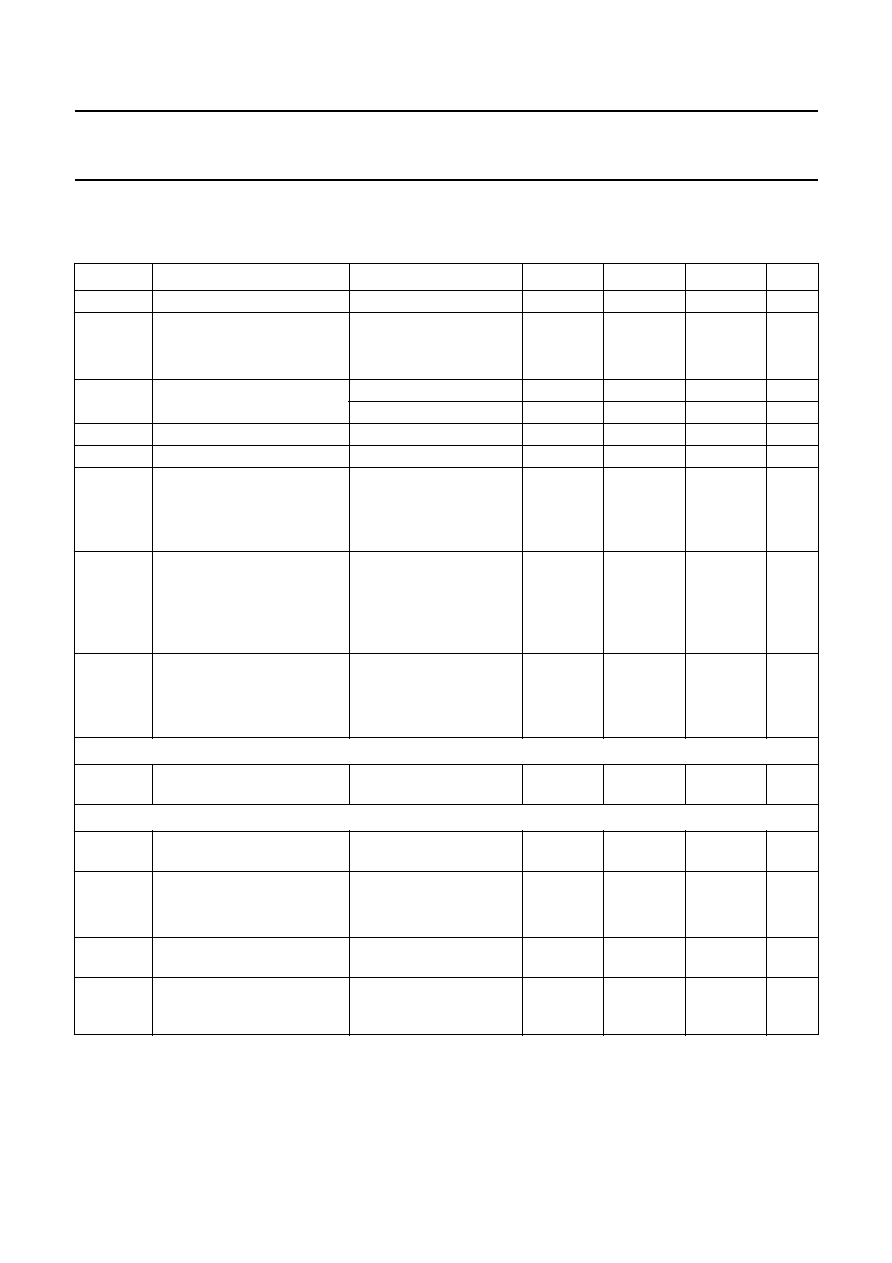
handbook, halfpage
3.0
5.5
1.130
1.127
MGT553
1.128
1.129
Vo(cm)
(V)
3.5
4.0
4.5
5.0
(1)
(2)
VCC (V)
Fig.11 Common mode voltage at the output as a
function of supply voltage.
(1) V
CC
-
V
OUT
.
(2) V
CC
-
V
OUTQ
.
handbook, halfpage
-
40
0
40
120
1.155
1.095
1.135
1.145
MGT554
80
(1)
(2)
Tj (
∞
C)
1.125
1.115
1.105
Vo(cm)
(V)
Fig.12 The common mode voltage at the output as
a function of the junction temperature.
V
CC
= 5 V.
(1) V
CC
-
V
OUT
.
(2) V
CC
-
V
OUTQ
.
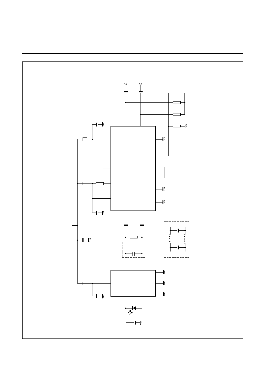
APPLICATION INFORMATION
handbook, full pagewidth
2
MGR370
1
8
VCC
DREF
3
IPhoto
GND
4
GND
5
GND
TZA3033T
7
OUTQ
6
OUT
R4
50
R3
50
Zo = 50
Zo = 50
22 nF
1 nF
680 nF
10
µ
H
VP
100 nF
100 nF
Fig.13 Application diagram.
2002
Sep
06
13
Philips Semiconductors
Product specification
SDH/SONET STM1/OC3
tr
ansimpedance amplifier
TZA3033
This text is here in white to force landscape pages to be rotated correctly when browsing through the pdf in the Acrobat reader.This text is here in
_
white to force landscape pages to be rotated correctly when browsing through the pdf in the Acrobat reader.This text is here inThis text is here in
white to force landscape pages to be rotated correctly when browsing through the pdf in the Acrobat reader. white to force landscape pages to be ...
handbook, full pagewidth
MGT555
(23) 12
DOUTQ
6
OUT
7
OUTQ
(24) 13
DOUT
1 k
50
50
10 nF
10 nF
100 nF
100 nF
100 nF
31 pF
noise filter:
1-pole, 100 MHz
100
135 k
TZA3033T
TZA3034
(1, 14)
1
(19, 20, 22, 25)
11
SUB
(16)
8
JAM
(17)
9
STQ
(18)
10
ST
(3, 4, 6, 9)
3
AGND
8
VCC
VCC
6
(11, 12)
VCCA
16
(30)
RSET
7
(13)
CF
15
(29)
Vref
14
(27, 28)
VCCD
DGND
data out
level detect
status
VCC
-
2 V
5 (8)
DINQ
4 (7)
DIN
3
1
22 nF
680 nF
100 nF
29.2
pF
4.5
pF
64.4 nH
64.4 nH
optional noise filter:
3-pole, 120 MHz Bessel
(1)
(1)
(1)
2
GND
4
GND
5
GND
100
nF
IPhoto
DREF
Fig.14 STM1/OC3 receiver using the TZA3033 and TZA3034.
(1) Ferrite bead e.g. Murata BLM10A700S.
2002 Sep 06
14
Philips Semiconductors
Product specification
SDH/SONET STM1/OC3
transimpedance amplifier
TZA3033
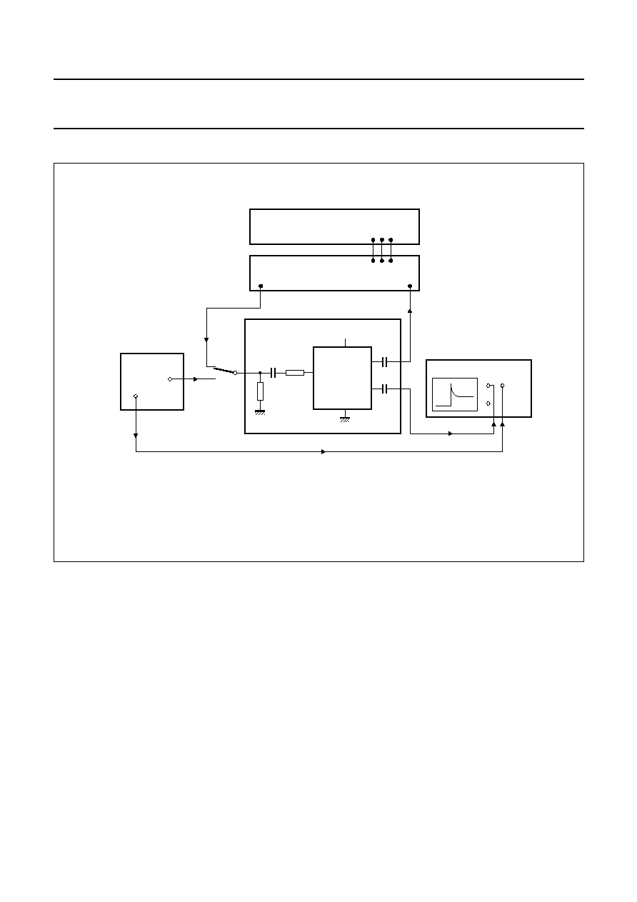
Test circuits
handbook, full pagewidth
MGT556
1 k
R
51
Zo = 50
Zo = 50
Zo = 50
IN
GND
OUT
OUTQ
10 nF
VCC
100 nF
trigger
input
1
SAMPLING OSC
2
PORT 1
PORT 2
NETWORK ANALYZER
S-PARAMETER TEST SET
100 nF
TZA3033T
PATTERN
GENERATOR
2
23
-
1 PRBS
DATA
2
23
-
1 PRBS CLOCK
Fig.15 Test circuit.
Total impedance of the test circuit is Z
T
and is calculated by the equation Z
T
= S
21
x (R + Z
IN
) x 2
where S
21
is the insertion loss of ports 1 and 2.
Typical values: R = 1 k
, Z
IN
= 330
.
2002 Sep 06
15
Philips Semiconductors
Product specification
SDH/SONET STM1/OC3
transimpedance amplifier
TZA3033
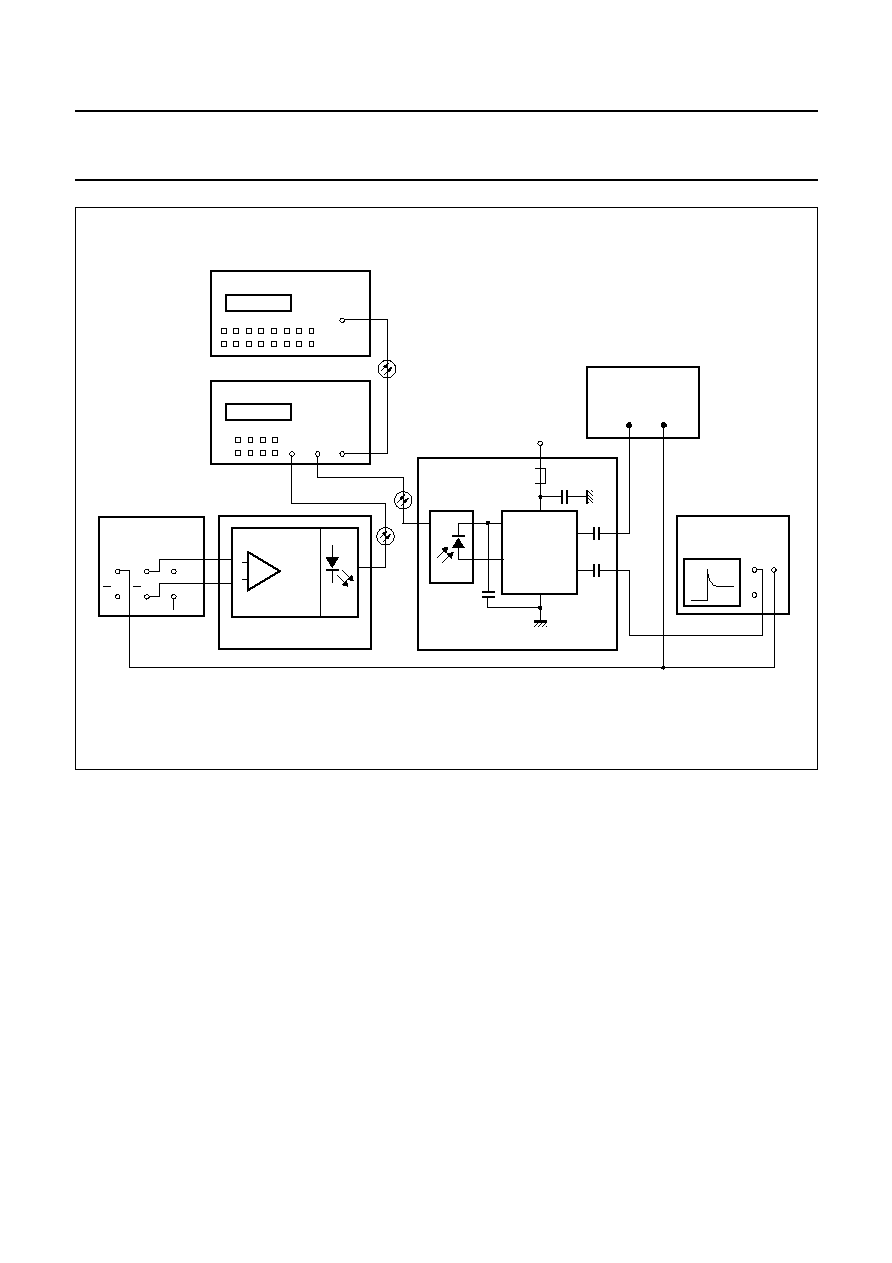
handbook, full pagewidth
MGT557
Zo = 50
Zo =
50
IPhoto
PIN
DREF
DIN
DINQ
0 dBm/1300
Laser
IN
OUT
OPTICAL
INPUT
OUT
OUTQ
TR
D
VCC
100 nF
BLM
22 nF
10 nF
10%
90%
Data
in
Clock
in
ERROR DETECTOR
TR
1
2
100 nF
TZA3033
TZA3041
OM5804
OM5802
PATTERN
GENERATOR
LASER DRIVER
OPTICAL ATTENUATOR
LIGHTWAVE MULTIMETER
155.520 Mb/s
2
23
-1 PRBS
C IN
D
C
C
-
9.54 dBm
SAMPLING
OSCILLOSCOPE/
TDR/TDT
Fig.16 Optical test circuit.
2002 Sep 06
16
Philips Semiconductors
Product specification
SDH/SONET STM1/OC3
transimpedance amplifier
TZA3033
handbook, full pagewidth
MGT558
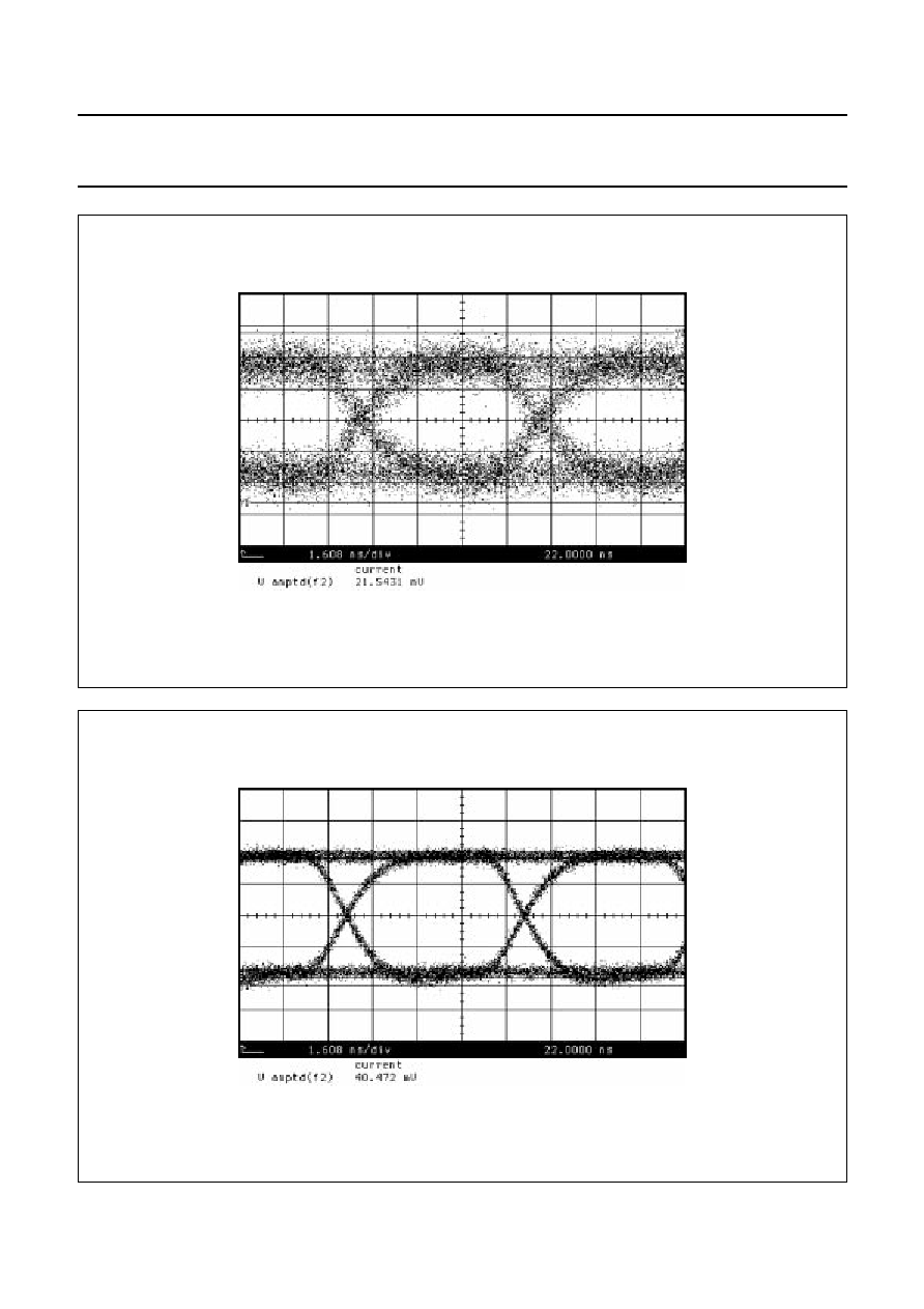
Fig.17 Differential output with
-
35 dBm optical input power [input current of 0.517
µ
A (p-p)].
handbook, full pagewidth
MGT559
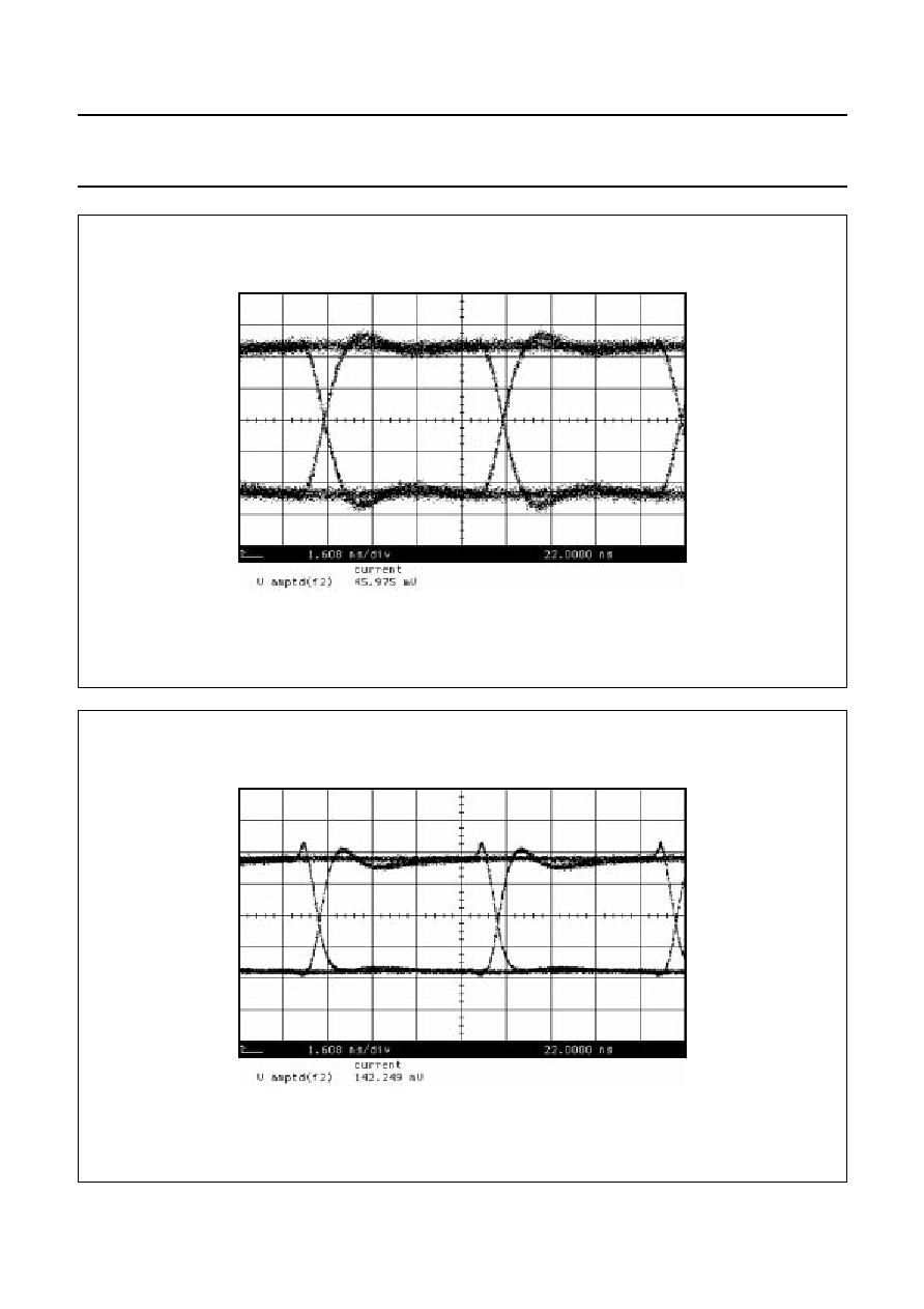
Fig.18 Differential output with
-
25 dBm optical input power [input current of 5.17
µ
A (p-p)].
2002 Sep 06
17
Philips Semiconductors
Product specification
SDH/SONET STM1/OC3
transimpedance amplifier
TZA3033
handbook, full pagewidth
MGT560
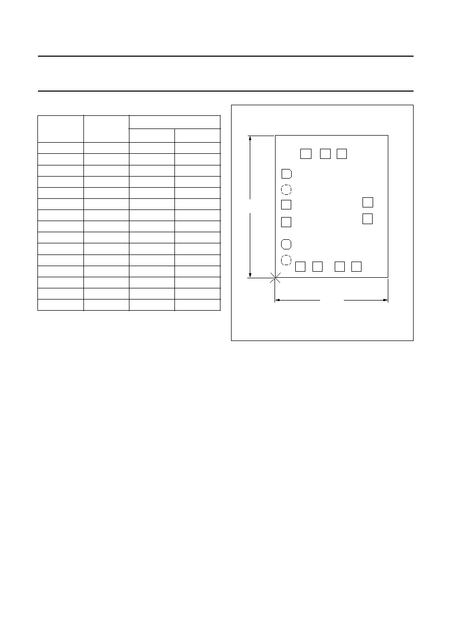
Fig.19 Differential output with
-
15 dBm optical input power [input current of 51.7
µ
A (p-p)].
handbook, full pagewidth
MGT561
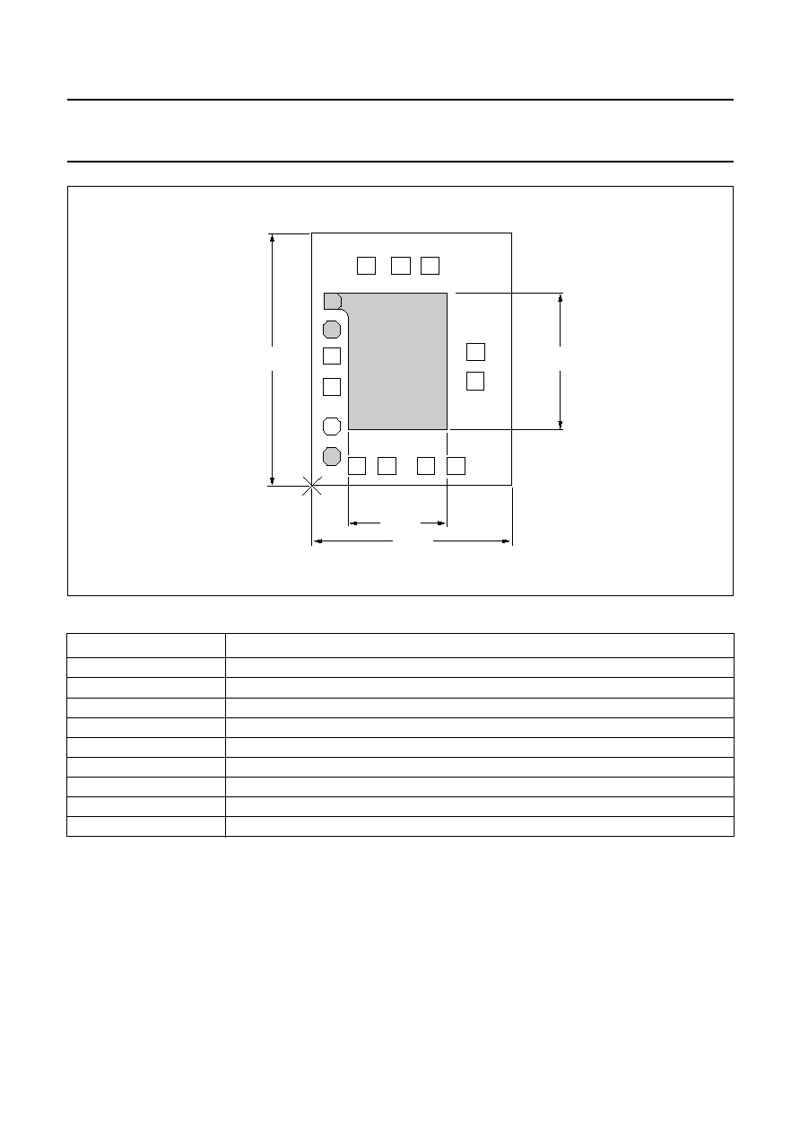
Fig.20 Differential output with
-
2 dBm optical input power [input current of 1030
µ
A (p-p)].
2002 Sep 06
18
Philips Semiconductors
Product specification
SDH/SONET STM1/OC3
transimpedance amplifier
TZA3033
BONDING PAD LOCATIONS
Note
1. All coordinates are referenced, in
µ
m, to the bottom
left-hand corner of the die.
SYMBOL
PAD
COORDINATES
(1)
x
y
DREF
1
95
881
TESTA
2
95
735
GND
3
95
618
GND
4
95
473
IPhoto
5
95
285
TESTB
6
95
147
GND
7
215
95
GND
8
360
95
GND
9
549
95
GND
10
691
95
OUT
11
785
501
OUTQ
12
785
641
V
CC
13
567
1055
V
CC
14
424
1055
AGC
15
259
1055
TZA3033U
1
12
11
3
4
5
7
0
x
y
0
15
14
13
8
9
10
1300
µ
m
1030
µ
m
DREF
IPhoto
GND
2
TESTA
6
TESTB
GND
OUTQ
OUT
MGT563
GND
GND
AGC
V
CC
V
CC
GND
GND
Fig.21 Bonding pad locations of the TZA3033U.
2002 Sep 06
19
Philips Semiconductors
Product specification
SDH/SONET STM1/OC3
transimpedance amplifier
TZA3033
handbook, full pagewidth
1
12
11
3
2
4
5
7
0
x
y
0
15
14
13
8
6
9
10
1300
µ
m
725
µ
m
1030
µ
m
455
µ
m
DREF
IPhoto
GND
GND
OUTQ
OUT
MCE068
GND
GND
AGC
V
CC
V
CC
GND
GND
TZA3033U/G
Fig.22 Bonding pad plus gold plate locations of the TZA3033U/G.
Physical characteristics of the bare die
Note
1. For the TZA3033U/G version only.
PARAMETER
VALUE
Gold layer
(1)
2.8
µ
m Au + 3.2
µ
m TiW
Glass passivation
2.1
µ
m PhosphoSilicate Glass (PSG) on top of 0.65
µ
m oxynitride
Bonding pad dimension
minimum dimension of exposed metallization is 90
◊
90
µ
m (pad size = 100
◊
100
µ
m)
Metallization
1.22
µ
m W/AlCu/TiW
Thickness
380
µ
m nominal
Size
1.03
◊
1.30 mm (1.34 mm
2
)
Backing
silicon; electrically connected to GND potential through substrate contacts
Attach temperature
<440
∞
C; recommended die attach is glue
Attach time
<15 s
2002 Sep 06
20
Philips Semiconductors
Product specification
SDH/SONET STM1/OC3
transimpedance amplifier
TZA3033
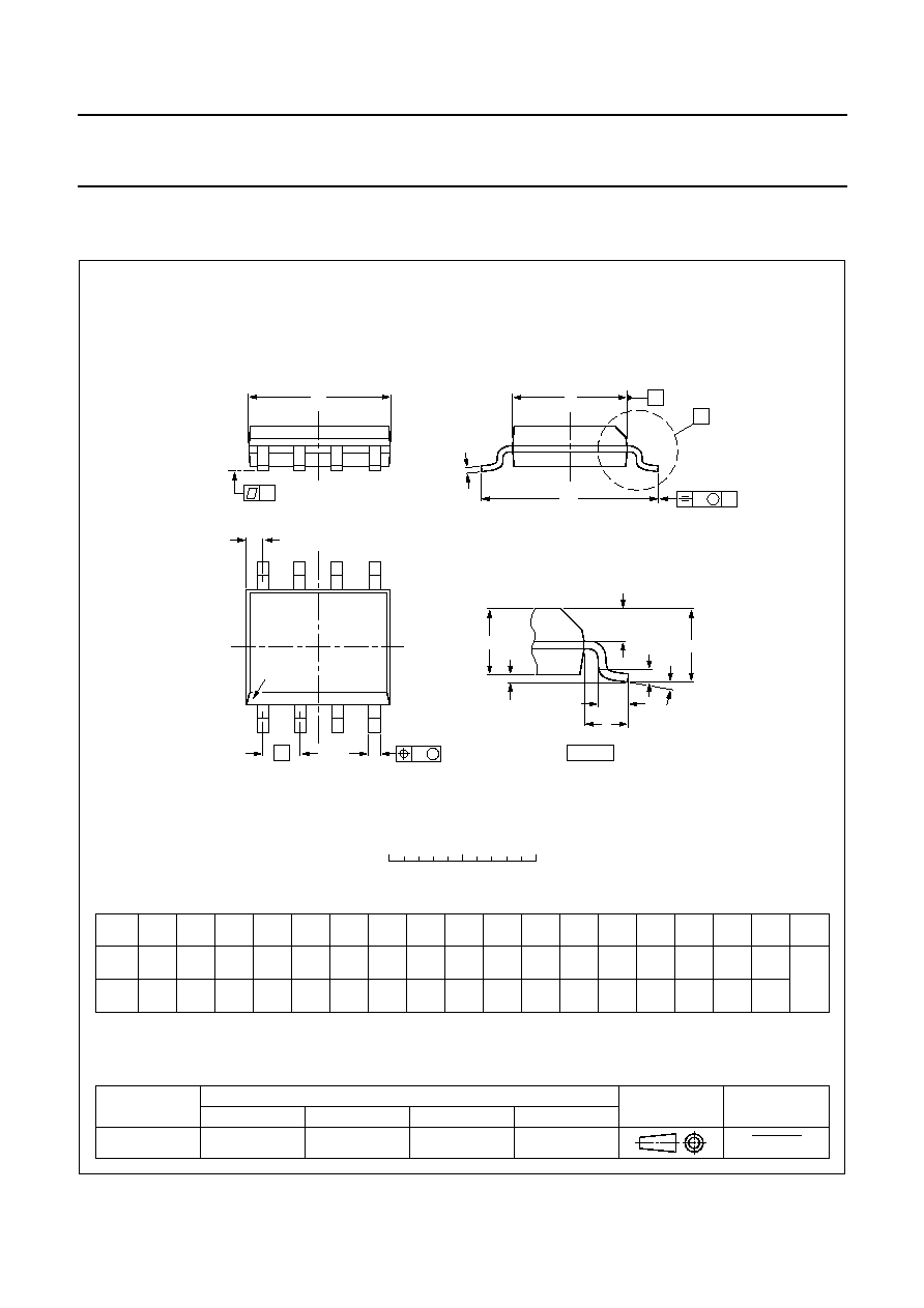
PACKAGE OUTLINE
UNIT
A
max.
A
1
A
2
A
3
b
p
c
D
(1)
E
(2)
(1)
e
H
E
L
L
p
Q
Z
y
w
v
REFERENCES
OUTLINE
VERSION
EUROPEAN
PROJECTION
ISSUE DATE
IEC
JEDEC
EIAJ
mm
inches
1.75
0.25
0.10
1.45
1.25
0.25
0.49
0.36
0.25
0.19
5.0
4.8
4.0
3.8
1.27
6.2
5.8
1.05
0.7
0.6
0.7
0.3
8
0
o
o
0.25
0.1
0.25
DIMENSIONS (inch dimensions are derived from the original mm dimensions)
Notes
1. Plastic or metal protrusions of 0.15 mm maximum per side are not included.
2. Plastic or metal protrusions of 0.25 mm maximum per side are not included.
1.0
0.4
SOT96-1
X
w
M
A
A
1
A
2
b
p
D
H
E
L
p
Q
detail X
E
Z
e
c
L
v
M
A
(A )
3
A
4
5
pin 1 index
1
8
y
076E03
MS-012
0.069
0.010
0.004
0.057
0.049
0.01
0.019
0.014
0.0100
0.0075
0.20
0.19
0.16
0.15
0.050
0.244
0.228
0.028
0.024
0.028
0.012
0.01
0.01
0.041
0.004
0.039
0.016
0
2.5
5 mm
scale
SO8: plastic small outline package; 8 leads; body width 3.9 mm
SOT96-1
97-05-22
99-12-27

2002 Sep 06
21
Philips Semiconductors
Product specification
SDH/SONET STM1/OC3
transimpedance amplifier
TZA3033
SOLDERING
Introduction to soldering surface mount packages
This text gives a very brief insight to a complex technology.
A more in-depth account of soldering ICs can be found in
our
"Data Handbook IC26; Integrated Circuit Packages"
(document order number 9398 652 90011).
There is no soldering method that is ideal for all surface
mount IC packages. Wave soldering can still be used for
certain surface mount ICs, but it is not suitable for fine pitch
SMDs. In these situations reflow soldering is
recommended.
Reflow soldering
Reflow soldering requires solder paste (a suspension of
fine solder particles, flux and binding agent) to be applied
to the printed-circuit board by screen printing, stencilling or
pressure-syringe dispensing before package placement.
Several methods exist for reflowing; for example,
convection or convection/infrared heating in a conveyor
type oven. Throughput times (preheating, soldering and
cooling) vary between 100 and 200 seconds depending
on heating method.
Typical reflow peak temperatures range from
215 to 250
∞
C. The top-surface temperature of the
packages should preferable be kept below 220
∞
C for
thick/large packages, and below 235
∞
C for small/thin
packages.
Wave soldering
Conventional single wave soldering is not recommended
for surface mount devices (SMDs) or printed-circuit boards
with a high component density, as solder bridging and
non-wetting can present major problems.
To overcome these problems the double-wave soldering
method was specifically developed.
If wave soldering is used the following conditions must be
observed for optimal results:
∑
Use a double-wave soldering method comprising a
turbulent wave with high upward pressure followed by a
smooth laminar wave.
∑
For packages with leads on two sides and a pitch (e):
≠ larger than or equal to 1.27 mm, the footprint
longitudinal axis is preferred to be parallel to the
transport direction of the printed-circuit board;
≠ smaller than 1.27 mm, the footprint longitudinal axis
must be parallel to the transport direction of the
printed-circuit board.
The footprint must incorporate solder thieves at the
downstream end.
∑
For packages with leads on four sides, the footprint must
be placed at a 45
∞
angle to the transport direction of the
printed-circuit board. The footprint must incorporate
solder thieves downstream and at the side corners.
During placement and before soldering, the package must
be fixed with a droplet of adhesive. The adhesive can be
applied by screen printing, pin transfer or syringe
dispensing. The package can be soldered after the
adhesive is cured.
Typical dwell time is 4 seconds at 250
∞
C.
A mildly-activated flux will eliminate the need for removal
of corrosive residues in most applications.
Manual soldering
Fix the component by first soldering two
diagonally-opposite end leads. Use a low voltage (24 V or
less) soldering iron applied to the flat part of the lead.
Contact time must be limited to 10 seconds at up to
300
∞
C.
When using a dedicated tool, all other leads can be
soldered in one operation within 2 to 5 seconds between
270 and 320
∞
C.

2002 Sep 06
22
Philips Semiconductors
Product specification
SDH/SONET STM1/OC3
transimpedance amplifier
TZA3033
Suitability of surface mount IC packages for wave and reflow soldering methods
Notes
1. For more detailed information on the BGA packages refer to the
"(LF)BGA Application Note" (AN01026); order a copy
from your Philips Semiconductors sales office.
2. All surface mount (SMD) packages are moisture sensitive. Depending upon the moisture content, the maximum
temperature (with respect to time) and body size of the package, there is a risk that internal or external package
cracks may occur due to vaporization of the moisture in them (the so called popcorn effect). For details, refer to the
Drypack information in the
"Data Handbook IC26; Integrated Circuit Packages; Section: Packing Methods".
3. These packages are not suitable for wave soldering. On versions with the heatsink on the bottom side, the solder
cannot penetrate between the printed-circuit board and the heatsink. On versions with the heatsink on the top side,
the solder might be deposited on the heatsink surface.
4. If wave soldering is considered, then the package must be placed at a 45
∞
angle to the solder wave direction.
The package footprint must incorporate solder thieves downstream and at the side corners.
5. Wave soldering is suitable for LQFP, TQFP and QFP packages with a pitch (e) larger than 0.8 mm; it is definitely not
suitable for packages with a pitch (e) equal to or smaller than 0.65 mm.
6. Wave soldering is suitable for SSOP and TSSOP packages with a pitch (e) equal to or larger than 0.65 mm; it is
definitely not suitable for packages with a pitch (e) equal to or smaller than 0.5 mm.
PACKAGE
(1)
SOLDERING METHOD
WAVE
REFLOW
(2)
BGA, LBGA, LFBGA, SQFP, TFBGA, VFBGA
not suitable
suitable
HBCC, HBGA, HLQFP, HSQFP, HSOP, HTQFP, HTSSOP, HVQFN,
HVSON, SMS
not suitable
(3)
suitable
PLCC
(4)
, SO, SOJ
suitable
suitable
LQFP, QFP, TQFP
not recommended
(4)(5)
suitable
SSOP, TSSOP, VSO
not recommended
(6)
suitable

2002 Sep 06
23
Philips Semiconductors
Product specification
SDH/SONET STM1/OC3
transimpedance amplifier
TZA3033
DATA SHEET STATUS
Notes
1. Please consult the most recently issued data sheet before initiating or completing a design.
2. The product status of the device(s) described in this data sheet may have changed since this data sheet was
published. The latest information is available on the Internet at URL http://www.semiconductors.philips.com.
DATA SHEET STATUS
(1)
PRODUCT
STATUS
(2)
DEFINITIONS
Objective data
Development
This data sheet contains data from the objective specification for product
development. Philips Semiconductors reserves the right to change the
specification in any manner without notice.
Preliminary data
Qualification
This data sheet contains data from the preliminary specification.
Supplementary data will be published at a later date. Philips
Semiconductors reserves the right to change the specification without
notice, in order to improve the design and supply the best possible
product.
Product data
Production
This data sheet contains data from the product specification. Philips
Semiconductors reserves the right to make changes at any time in order
to improve the design, manufacturing and supply. Changes will be
communicated according to the Customer Product/Process Change
Notification (CPCN) procedure SNW-SQ-650A.

2002 Sep 06
24
Philips Semiconductors
Product specification
SDH/SONET STM1/OC3
transimpedance amplifier
TZA3033
DEFINITIONS
Short-form specification
The data in a short-form
specification is extracted from a full data sheet with the
same type number and title. For detailed information see
the relevant data sheet or data handbook.
Limiting values definition
Limiting values given are in
accordance with the Absolute Maximum Rating System
(IEC 60134). Stress above one or more of the limiting
values may cause permanent damage to the device.
These are stress ratings only and operation of the device
at these or at any other conditions above those given in the
Characteristics sections of the specification is not implied.
Exposure to limiting values for extended periods may
affect device reliability.
Application information
Applications that are
described herein for any of these products are for
illustrative purposes only. Philips Semiconductors make
no representation or warranty that such applications will be
suitable for the specified use without further testing or
modification.
DISCLAIMERS
Life support applications
These products are not
designed for use in life support appliances, devices, or
systems where malfunction of these products can
reasonably be expected to result in personal injury. Philips
Semiconductors customers using or selling these products
for use in such applications do so at their own risk and
agree to fully indemnify Philips Semiconductors for any
damages resulting from such application.
Right to make changes
Philips Semiconductors
reserves the right to make changes, without notice, in the
products, including circuits, standard cells, and/or
software, described or contained herein in order to
improve design and/or performance. Philips
Semiconductors assumes no responsibility or liability for
the use of any of these products, conveys no licence or title
under any patent, copyright, or mask work right to these
products, and makes no representations or warranties that
these products are free from patent, copyright, or mask
work right infringement, unless otherwise specified.
Bare die
All die are tested and are guaranteed to
comply with all data sheet limits up to the point of wafer
sawing for a period of ninety (90) days from the date of
Philips' delivery. If there are data sheet limits not
guaranteed, these will be separately indicated in the data
sheet. There are no post packing tests performed on
individual die or wafer. Philips Semiconductors has no
control of third party procedures in the sawing, handling,
packing or assembly of the die. Accordingly, Philips
Semiconductors assumes no liability for device
functionality or performance of the die or systems after
third party sawing, handling, packing or assembly of the
die. It is the responsibility of the customer to test and
qualify their application in which the die is used.

2002 Sep 06
25
Philips Semiconductors
Product specification
SDH/SONET STM1/OC3
transimpedance amplifier
TZA3033
NOTES

2002 Sep 06
26
Philips Semiconductors
Product specification
SDH/SONET STM1/OC3
transimpedance amplifier
TZA3033
NOTES

2002 Sep 06
27
Philips Semiconductors
Product specification
SDH/SONET STM1/OC3
transimpedance amplifier
TZA3033
NOTES

© Koninklijke Philips Electronics N.V. 2002
SCA74
All rights are reserved. Reproduction in whole or in part is prohibited without the prior written consent of the copyright owner.
The information presented in this document does not form part of any quotation or contract, is believed to be accurate and reliable and may be changed
without notice. No liability will be accepted by the publisher for any consequence of its use. Publication thereof does not convey nor imply any license
under patent- or other industrial or intellectual property rights.
Philips Semiconductors ≠ a worldwide company
Contact information
For additional information please visit http://www.semiconductors.philips.com.
Fax: +31 40 27 24825
For sales offices addresses send e-mail to: sales.addresses@www.semiconductors.philips.com.
Printed in The Netherlands
403510/03/pp
28
Date of release:
2002 Sep 06
Document order number:
9397 750 10127