 | –≠–ª–µ–∫—Ç—Ä–æ–Ω–Ω—ã–π –∫–æ–º–ø–æ–Ω–µ–Ω—Ç: UAA3500HL | –°–∫–∞—á–∞—Ç—å:  PDF PDF  ZIP ZIP |

DATA SHEET
Preliminary specification
Supersedes data of 1999 Mar 30
File under Integrated Circuits, IC17
2000 Jan 18
INTEGRATED CIRCUITS
UAA3500HL
Pager receiver

2000 Jan 18
2
Philips Semiconductors
Preliminary specification
Pager receiver
UAA3500HL
FEATURES
∑
Double frequency conversion, zero-IF receiver with:
≠ Configurable in all paging bands (130 to 930 MHz)
≠ Low noise amplifier featured with four step Automatic
Gain Control (AGC)
≠ Down-conversion mixers
≠ On-chip, zero-IF channel filter
≠ I/Q, non-demodulated outputs
≠ Highpass filters to remove DC offsets.
∑
External Voltage Controlled Oscillator (VCO):
≠ Both Local Oscillators (LOs) derived from the VCO.
APPLICATIONS
∑
FLEX
TM
, ERMES and POCSAG pagers
∑
Remote control terminals.
GENERAL DESCRIPTION
The UAA3500HL is a one-chip pager receiver complying
with POCSAG, FLEX
TM
and ERMES standards. The IC
performs in accordance with specifications in the
-
10 to +55
∞
C temperature range.
The UAA3500HL contains a front-end receiver, which can
be configured through external components for any
frequency band between 130 and 930 MHz. The back-end
receiver consists of the channel filter and limiters. An
external VCO ensures the Local Oscillator (LO) for the
front-end. Designed in an advanced BiCMOS process, it
combines high performance with low-power consumption
and a high degree of integration, thus reducing external
component costs and total radio size.
Its first advantage is to remove the expensive SAW filter
necessary in a superhet architecture, replacing it by an
integrated, elliptic channel filter that provides 70 dB
adjacent channel rejection. The receive front-end section
consists of a low-noise amplifier that drives mixers through
an external LC image rejection filter. The output drives the
I and Q second mixers, whose outputs are at zero
frequency. The receiver back-end section consists of
filters (channel filtering), limiters (limited output required)
and high-pass filters (DC block) to remove DC offsets.
Outputs are I and Q, undemodulated signals.
Its second advantage is to provide the two LO signals from
one VCO only, tuned by a PLL. An on-chip frequency
divider-by-2 and buffers provide the LO sources.
Its third advantage is to provide two voltage regulators,
allowing to obtain 1.0 and 1.8 V regulated voltages.
ORDERING INFORMATION
TYPE NUMBER
PACKAGE
NAME
DESCRIPTION
VERSION
UAA3500HL
LQFP48
plastic low profile quad flat package; 48 leads; body 7
◊
7
◊
1.4 mm
SOT313-2

2000 Jan 18
3
Philips Semiconductors
Preliminary specification
Pager receiver
UAA3500HL
QUICK REFERENCE DATA
Notes
1. For 930 MHz band; for other conditions see Chapters "DC characteristics" and "AC characteristics".
2. For B+ and B++, see Fig.3.
SYMBOL
PARAMETER
CONDITIONS
(1)
MIN.
TYP.
MAX. UNIT
V
CC1
supply voltage 1
(B++;see note 2)
1.85
2.1
3.3
V
V
CC2
supply voltage 2
(B+; see note 2)
1.05
1.4
1.5
V
I
CC1(RX)
supply current from B++
RX section on; DC tested
f
RF
= 160 MHz
-
2.4
-
mA
f
RF
= 280 MHz
-
2.4
-
mA
f
RF
= 930 MHz
2.35
2.7
3
mA
I
CC2(RX)
supply current from B+
RX section on; DC tested
f
RF
= 160 MHz
-
1.3
-
mA
f
RF
= 280 MHz
-
1.4
-
mA
f
RF
= 930 MHz
1.85
2.3
2.45
mA
NF
RX
receiver noise figure
from RF input to 2nd mixer input
f
RF
= 160 MHz
-
2.7
-
dB
f
RF
= 280 MHz
-
3.1
-
dB
f
RF
= 930 MHz
-
4.4
-
dB
P
i(ref)
RF input sensitivity
3% BER
f
RF
= 160 MHz; 1600 bits/s 2-level FSK
-
-
128.5
-
dBm
f
RF
= 280 MHz; 1600 bits/s 2-level FSK
-
-
128
-
dBm
f
RF
= 930 MHz; 6400 bits/s 2-level FSK
-
-
126.5
-
dBm
f
RF
= 930 MHz; 6400 bits/s 4-level FSK
-
-
123
-
dBm
ACR
adjacent channel rejection
65
70
-
dB
T
amb
ambient temperature
-
10
+25
+55
∞
C
2000
Jan
18
4
Philips Semiconductors
Preliminar
y specification
P
ager receiv
er
U
AA3500HL
This text is here in white to force landscape pages to be rotated correctly when browsing through the pdf in the Acrobat reader.This text is here in
_
white to force landscape pages to be rotated correctly when browsing through the pdf in the Acrobat reader.This text is here inThis text is here in
white to force landscape pages to be rotated correctly when browsing through the pdf in the Acrobat reader. white to force landscape pages to be ...
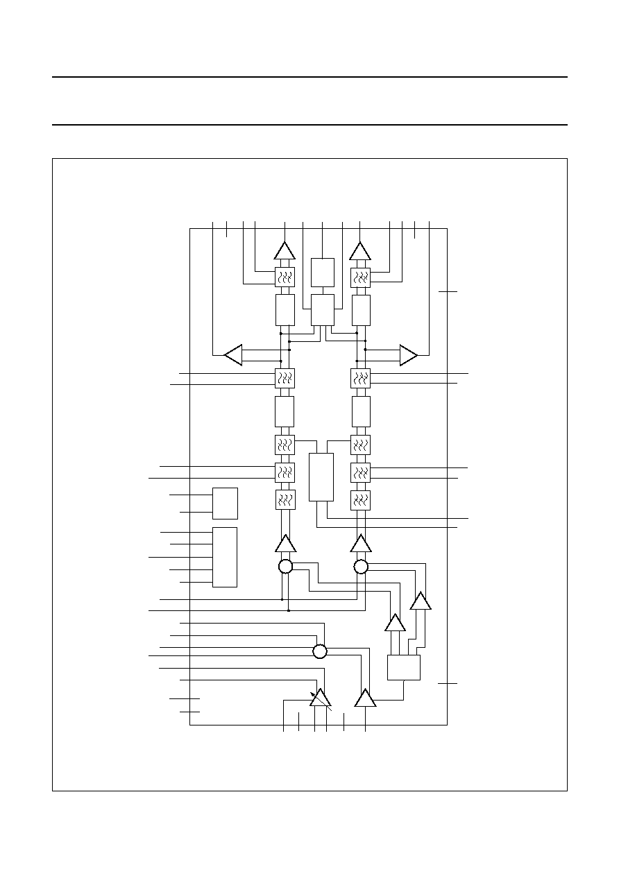
BLOCK DIA
GRAM
handbook, full pagewidth
VOLTAGE
REGULATOR
LNA
AGC
RSSI
RSSI
FCA022
OUTPUT
OUTPUT
2
0
PMA
LIMITER
PMA
BIAS
LIMITER
LIMITER
LIMITER
OUTI
OUTQ
◊
◊
◊
RSET
LNAGND1
LNAGND2
RFINA
RFINB
LOIN
LOGND
BEGND
OGND
VCC(O)
UAA3500HL
IMINA
IMINB
IMOUTA
IMOUTB
FILINA
FILINB
FILOUTA
FILOUTB
DRV1
VCC(FE)
VCC(DC)
DRV2
VCC(LO)
FASTON
CAPI2B
CAPI1B
CAPI2A
CAPI1A
RXON
M2GND
40
37
33
32
31
30
29
21
42 41 46 47
16 17 18 25 24
28
23
43 44
3
4
45
5
2
1
6
26
34
27
7
11
12
8
15
39
38
36
35
22
14
13
20
19
10
9
48
M1GND
GYROUTI
GYROUTQ
BUFFER
BUFFER
BUFFER
BUFFER
BUFFER
90
AGCADJ
AGCTAU
CAPI3A
CAPI3B
CAPQ3A
CAPQ3B
CAPQ2A
CAPQ1A
CAPQ2B
CAPQ1B
GYRATOR
REGULATOR
GYRCO1
GYRCO2
Fig.1 Block diagram.

2000 Jan 18
5
Philips Semiconductors
Preliminary specification
Pager receiver
UAA3500HL
PINNING
SYMBOL
PIN
DESCRIPTION
CAPI3B
1
3rd DC filter (I path) external capacitor B (I path)
CAPI3A
2
3rd DC filter (I path) external capacitor A (I path)
CAPI2A
3
2nd DC filter (I path) external capacitor A (I path)
CAPI2B
4
2nd DC filter (I path) external capacitor A (I path)
V
CC(O)
5
output stage supply voltage B++ (I path)
OUTI
6
output I and Q signals (I path)
OUTQ
7
output I and Q signals (Q path)
OGND
8
output stage ground
CAPQ2B
9
2nd DC filter external capacitor B (Q path)
CAPQ2A
10
2nd DC filter external capacitor A (Q path)
CAPQ3A
11
3rd DC filter external capacitor A (Q path)
CAPQ3B
12
3rd DC filter external capacitor B (Q path)
GYRCO2
13
external resistor to set-up gyrator filter cut-off frequency
GYRCO1
14
external resistor to set-up gyrator filter cut-off frequency
GYROUTQ
15
Q-gyrator output
DRV1
16
regulator driver (1.8 V)
V
CC(FE)
17
regulated voltage for front-end (1.8 V)
V
CC(DC)
18
input voltage from DC-to-DC converter (2.1 V)
CAPQ1B
19
1st DC filter external capacitor (Q path)
CAPQ1A
20
1st DC filter external capacitor (Q path)
LOIN
21
LO input
LOGND
22
LO strip ground
FASTON
23
fast mode enable
V
CC(LO)
24
regulated voltage for LO strip (1.0 V)
DRV2
25
regulator driver (1.0)
AGCADJ
26
AGC loop gain control
AGCTAU
27
AGC loop time constant
RXON
28
receiver mode enable
LNAGND1
29
receiver LNA (Low Noise Amplifier) ground 1
RFINB
30
LNA input B
RFINA
31
LNA input A
LNAGND2
32
receiver LNA ground 2
RSET
33
LNA current setup
RSSI
34
received signal strength indicator
IMINA
35
image rejection filter input A
IMINB
36
image rejection filter input B
M1GND
37
first mixer ground
IMOUTA
38
image rejection filter output A
IMOUTB
39
image rejection filter output B
M2GND
40
second mixers ground
2000 Jan 18
6
Philips Semiconductors
Preliminary specification
Pager receiver
UAA3500HL
FILINB
41
band filter input B
FILINA
42
band filter input A
CAPI1A
43
1st DC filter external capacitor (I path)
CAPI1B
44
1st DC filter external capacitor (I path)
GYROUTI
45
I-gyrator output
FILOUTA
46
band filter output to second mixers
FILOUTB
47
band filter output to second mixers
BEGND
48
receiver back-end ground
SYMBOL
PIN
DESCRIPTION
handbook, full pagewidth
UAA3500HL
FCA023
1
2
3
4
5
6
7
8
9
10
11
12
36
35
34
33
32
31
30
29
28
27
26
25
13
14
15
16
17
18
19
20
21
22
23
24
48
47
46
45
44
43
42
41
40
39
38
37
BEGND
FILOUTB
FILOUTA
GYROUTI
CAPI1B
CAPI1A
FILINA
FILINB
IMOUTB
M2GND
IMOUTA
M1GND
GYRCO2
GYRCO1
GYROUTQ
DRV1
V
CC(FE)
V
CC(DC)
CAPQ1B
CAPQ1A
LOIN
LOGND
FASTON
V
CC(LO)
CAPI3B
CAPI3A
CAPI2A
CAPI2B
VCC(O)
OUTI
OUTQ
OGND
CAPQ2B
CAPQ2A
CAPQ3A
CAPQ3B
IMINB
IMINA
RSSI
RSET
LNAGND2
RFINA
RFINB
LNAGND1
RXON
AGCTAU
AGCADJ
DRV2
Fig.2 Pin configuration.

2000 Jan 18
7
Philips Semiconductors
Preliminary specification
Pager receiver
UAA3500HL
FUNCTIONAL DESCRIPTION
Receiver front-end section
The receiver front-end consists of an LNA, followed by the
first and the second mixers. For operation at low frequency
(160 and 280 MHz, for instance), the first mixer can be
bypassed, saving some current. The image rejection is
done by an external LC filter placed between the LNA, the
first mixer and the antenna selectivity. The IF band is
filtered by an external filter placed between the first mixer
and the second mixers for the I and Q paths. The
RF signals are in phase, and the LO signals are shifted
by 90
∞
. The output signals are at zero frequency.
To increase the immunity to interferers, an AGC loop
controls the LNA gain by attenuating the RF input signal.
Four steps of attenuation are possible (each having 8 dB),
ranging therefore from 0 to 32 dB. The AGC loop
threshold level and time constant may be controlled
externally at pins AGCADJ and AGCTAU. The second
LO I/Q phase shift is made by a quadrature divider, whose
input is the VCO oscillating signal.
The LNA current is setup by an external resistor. All the
receivers (front-end and back-end) are turned on by
pin RXON.
Receiver back-end section
The down-converted signal is amplified and then filtered
by a Sallen-Key filter, which shows a notch at 15 kHz and
about 6 dB rejection out-of-band. Then comes the first
high-pass filter (DC block), followed by the gyrator filter,
which performs an elliptic, 7-pole low-pass filtering. The
signal is then amplified by the first limiter, filtered by the
second DC block, amplified again, and filtered again by
the third DC block. Finally, an output stage delivers the
signal with rail-to-rail logic levels.
The first, second and third DC block frequencies are set at
4, 8 and 12 Hz respectively by external 330 nF capacitors.
The two voltage regulators are also activated by RXON.
At the output of the gyrator filter, the signal is buffered and
logarithmically converted. It then controls the AGC loop.
To rapidly reach the DC operating point, a fast mode is
built into the three DC blocks.
LO
The external VCO is AC-coupled at input LOIN. It is then
buffered to drive the first mixer. LOIN also enters a
quadrature divider-by-2, whose output signals are also
buffered to drive the second mixers. The VCO frequency
should be
2
/
3
of the input RF signal.
The LO signal must be generated with an external
frequency synthesizer and VCO or with a crystal oscillator.
OPERATING MODES
To use the IC, all V
CC
pins must be connected to the
supply voltage B++ (2.1 V). The 1.8 V regulated voltage
sinks current from B++ and the 1.0 V regulated voltage
from B+ (1.4 V). In a typical application, the B+ supply is
the battery and the B++ supply is the DC/DC converter
located in the baseband chip.
In normal operating mode, the receiver should be
powered-on in fast mode. The fast mode can be turned off
after several milliseconds.
Table 1 gives the definition of the polarity of the switching
signals on the receive section.
Table 1
Switching signals on the receiver
SIGNAL
SECTION
LEVEL
ON/OFF
RXON
receive section powered-on
HIGH
on
receive section powered-off
LOW
off
FASTON
fast mode powered-on
HIGH
on
fast mode powered-off
LOW
off

2000 Jan 18
8
Philips Semiconductors
Preliminary specification
Pager receiver
UAA3500HL
LIMITING VALUES
In accordance with the Absolute Maximum Rating System (IEC 134).
Note
1. Pins short circuited internally must be short circuited externally.
THERMAL CHARACTERISTICS
HANDLING
All pins withstand the ESD test in accordance with
"MIL-STD-883C class 2 (method 3015.5)".
DC CHARACTERISTICS
V
CC
= 2.1 V; T
amb
= 25
∞
C; 930 MHz band application, 3% BER and 1600 bits/s 2 level; unless otherwise specified.
SYMBOL
PARAMETER
CONDITIONS
MIN.
MAX.
UNIT
V
CC
supply voltage
-
6
V
GND
difference in ground supply voltage applied between
all grounds
note 1
-
0.3
V
P
l(max)
maximum power input
-
20
dBm
T
j(max)
maximum operating junction temperature
-
150
∞
C
P
(max)
maximum power dissipation
in stagnant air at 25
∞
C
-
500
mW
T
stg
storage temperature
-
65
+150
∞
C
SYMBOL
PARAMETER
CONDITIONS
VALUE
UNIT
R
th(j-a)
thermal resistance from junction to ambient
in free air
90
K/W
SYMBOL
PARAMETER
CONDITIONS
MIN.
TYP.
MAX.
UNIT
Pins: V
CC(O)
, DRV1, V
CC(FE)
, V
CC(DC)
, V
CC(LO)
and DRV2
V
CC1
supply voltage 1
(B++; see note 1)
over full temperature range
1.85
2.1
3.3
V
V
CC2
supply voltage 2
(B+; see note 1)
over full temperature range
1.05
1.4
1.5
V
I
CC1(RX)
supply current from B++
RX section on; DC tested
f
RF
= 160 MHz
-
2.4
-
mA
f
RF
= 280 MHz
-
2.4
-
mA
f
RF
= 930 MHz
2.35
2.7
3
mA
I
CC2(RX)
supply current from B+
RX section on; DC tested
f
RF
= 160 MHz
-
1.3
-
mA
f
RF
= 280 MHz
-
1.4
-
mA
f
RF
= 930 MHz
1.85
2.3
2.45
mA
I
CC1(pd)
standby current from B++
Power-down mode; DC tested
0
0.01
1
µ
A
I
CC2(pd)
standby current from B+
Power-down mode; DC tested
0
0.01
0.5
µ
A

2000 Jan 18
9
Philips Semiconductors
Preliminary specification
Pager receiver
UAA3500HL
Note
1. For B+ and B++, see Fig.3.
Pins: RXON, FASTON, OUTI and OUTQ
V
IH
HIGH-level voltage
V
CC
-
0.3 V
CC
V
CC
+ 0.3
V
V
IL
LOW-level voltage
-
0.3
-
+0.4
V
I
IH
HIGH-level static current
V
CC
-
0.4 V
-
1
-
+1
µ
A
I
IL
LOW-level static current
pin at 0.4 V
-
1
-
+1
µ
A
Pins: CAPI1A, CAPI1B, CAPQ1A and CAPQ1B
V
CAP
DC level
RX section on
1.20
1.40
1.60
V
Pins: CAPI2A, CAPI2B, CAPQ2A, CAPQ2B
V
CAP
DC level
RX section on
1.40
1.57
1.80
V
Pins: CAPI3A, CAPI3B, CAPQ3A, CAPQ3B
V
CAP
DC level
RX section on
1.30
1.57
1.90
V
Pins: RFINA and RFINB
V
RF
DC level
RX section on
-
0.92
-
V
Pins: IMOUTA and IMOUTB
V
IMOUT
DC level
RX section on
-
0.17
-
V
Pins: V
CC(LO)
V
Vcc(lo)
DC level
RX section on
0.95
1.00
1.05
V
Pins: V
CC(FE)
V
Vcc(fe)
DC level
RX section on
1.75
1.80
1.85
V
Pins: FILOUTA and FILOUTB
V
FILOUT
DC level
RX section on
-
0.24
-
V
Pins: AGCTAU and RSSI
V
RSSI
DC level
RX section on; FASTON is LOW
-
0
0.30
V
RX section on;
FASTON is HIGH
V
CC
-
0.3 V
CC
-
V
V
AGCTAU
DC level
RX section on;
FASTON is HIGH
1.50
1.60
1.70
V
Pins: GYROUTI and GYROUTQ
V
GYROUT
DC level
RX section on
1.37
1.42
1.47
V
Output stage
V
OH
HIGH-level output voltage
I
o
=
-
5
µ
A
-
V
CC
-
0.2
-
V
V
OL
LOW-level output voltage
I
o
= 5
µ
A
-
0.2
-
V
SYMBOL
PARAMETER
CONDITIONS
MIN.
TYP.
MAX.
UNIT
2000 Jan 18
10
Philips Semiconductors
Preliminary specification
Pager receiver
UAA3500HL
AC CHARACTERISTICS
V
CC
= 2.1 V; T
amb
= 25
∞
C; 930 MHz band application, 3% BER and 1600 bits/s 2 level; on evaluation board according
to Fig.3; system measurement done using PCD5009, PCD5010 baseband; unless otherwise specified.
SYMBOL
PARAMETER
CONDITIONS
MIN.
TYP.
MAX. UNIT
Receiver
P
i(ref)
RF input sensitivity
3% BER
f
RF
= 160 MHz; 1600 bits/s 2-level FSK
-
-
128.5
-
dBm
f
RF
= 280 MHz; 1600 bits/s 2-level FSK
-
-
128
-
dBm
f
RF
= 930 MHz; 6400 bits/s 2-level FSK
-
-
126.5
-
dBm
f
RF
= 930 MHz; 6400 bits/s 4-level FSK
-
-
123
-
dBm
G
(PCFE)
front-end conversion power
gain
from RF input to 2nd mixer input
f
RF
= 160 MHz
-
20
-
dB
f
RF
= 280 MHz
-
12.8
-
dB
f
RF
= 930 MHz
-
12.7
-
dB
NF
RX
receiver noise figure
from RF input to 2nd mixer input
f
RF
= 160 MHz
-
2.7
-
dB
f
RF
= 280 MHz
-
3.1
-
dB
f
RF
= 930 MHz
-
4.4
-
dB
IP1
1 dB input compression point
from RF input to 2nd mixer input
-
-
38
-
dBm
IP2
2nd order intercept point
from 2nd mixer input to gyrator output
45
-
-
dBm
IP3
3rd order intercept point
from RF input to 2nd mixer input; note 1
-
-
33
-
dBm
IM3
3rd order intermodulation
3 signal measurement
55
-
-
dB
CCR
co-channel rejection
threshold +3 dB
-
5
-
dB
ACR
adjacent channel rejection
channel spacing = 25 kHz; from RF input
to gyrator output
65
70
-
dB
bl
blocking immunity
frequency offset >1 MHz
75
80
-
dB
G
AGC
front-end gain reduction by
AGC step
7
8
9
dB
AGC
th
AGC threshold
above sensitivity
20
25
30
dB
t
on
establishment time
until sensitivity +3 dB is reached
-
-
30
ms
IQ
IQ channel unbalance
-
-
2
dB
R
LNA
LNA current set resistor
160 MHz
-
56
-
k
280 MHz
-
47
-
k
930 MHz
-
27
-
k
R
gyr
gyrator cut-off frequency set
resistor
cut-off frequency = 8.5 kHz
-
47
-
k
LO
f
VCO
VCO frequency
-
2
/
3
f
RF
-
MHz
2000 Jan 18
11
Philips Semiconductors
Preliminary specification
Pager receiver
UAA3500HL
Note
1. The two tones for intermodulation test would normally be set at 2 and 4 or 4 and 8 channels for type approval tests
i.e 930 and 930.1 or 930.1 and 930.2 MHz.
LNA
G
LNA
RF amplifier power gain
from RF input to image filter output
f
RF
= 160 MHz
-
20
-
dB
f
RF
= 280 MHz
-
16.2
-
dB
f
RF
= 930 MHz
12.5
14.2
-
dB
NF
LNA
RF amplifier noise figure
from RF input to image filter output
f
RF
= 160 MHz
-
1.8
-
dB
f
RF
= 280 MHz
-
1.9
-
dB
f
RF
= 930 MHz
-
2.2
2.5
dB
IP1
LNA
1 dB input compression point
from RF input to image filter output
-
-
27
-
dBm
IP3
LNA
3rd order intercept point
from RF input to image filter output
-
21
-
17.6
-
dBm
First mixer
G
FM
1st mixer power gain
-
0.5
0
-
dB
NF
FM
1st mixer noise figure
-
10.2
13
dB
IP1
FM
1 dB input compression point
-
-
22
-
dBm
IP3
FM
3rd order intercept point
-
12.5
-
11
-
dBm
Second mixer, PMA, Sallen-Key, 1st DC block and gyrator filter
Gv
BE
voltage gain
from 2nd mixer input to gyrator output
42
45
-
dB
IP3
BE
3rd order intercept point
from 2nd mixer input to gyrator output
-
-
59
-
dBm
1st DC block
f
cut-off
cut-off frequency
measured at gyrator output;
FASTON is LOW
-
4
-
Hz
f
cut-off
cut-off frequency
measured at gyrator output;
FASTON is HIGH
150
400
-
Hz
SYMBOL
PARAMETER
CONDITIONS
MIN.
TYP.
MAX. UNIT
2000 Jan 18
12
Philips Semiconductors
Preliminary specification
Pager receiver
UAA3500HL
APPLICATION INFORMATION
handbook, full pagewidth
UAA3500HL
FCA024
1
CAP13B
CAP13A
CAP12A
IMINB
IMINA
RSSI
RSET
LNAGND2
RFINA
RFINB
RXON
AGCTAU
AGCADJ
DRV2
LNAGND1
CAP12B
VCC(O)
OUTI
OUTQ
OGND
CAPQ2B
CAPQ2A
CAPQ3A
CAPQ3B
GYRCO2
BEGND
FILOUTB
FILOUTA
GYROUTI
CAPI1B
CAPI1A
FILINA
FILINB
M2GND
IMOUTB
IMOUTA
M1GND
GYRCO1
GYROUTQ
DRV1
V
CC(FE)
V
CC(DC)
CAPQ1B
CAPQ1A
LOIN
LOGND
FASTON
V
CC(LO)
48
47
46
45
44
43
42
41
40
38
39
37
2
3
4
5
6
7
8
9
10
11
12
13
14
15
24
23
22
21
20
19
18
17
16
36
35
34
33
32
31
30
29
28
27
26
25
IMAGE
FILTER
BAND
FILTER
VCO
330 nF
330 nF
330 nF
330 nF
330 nF
B++
B++
330 nF
47 k
15
k
100 k
100
k
10
µ
F
10
µ
F
10 nF
10 nF
100 pF
GYROUTQ
FASTON
100 pF
B+
RXON
RLNA
RSSI
RFIN
GYROUTI
B++
OUTI
OUTQ
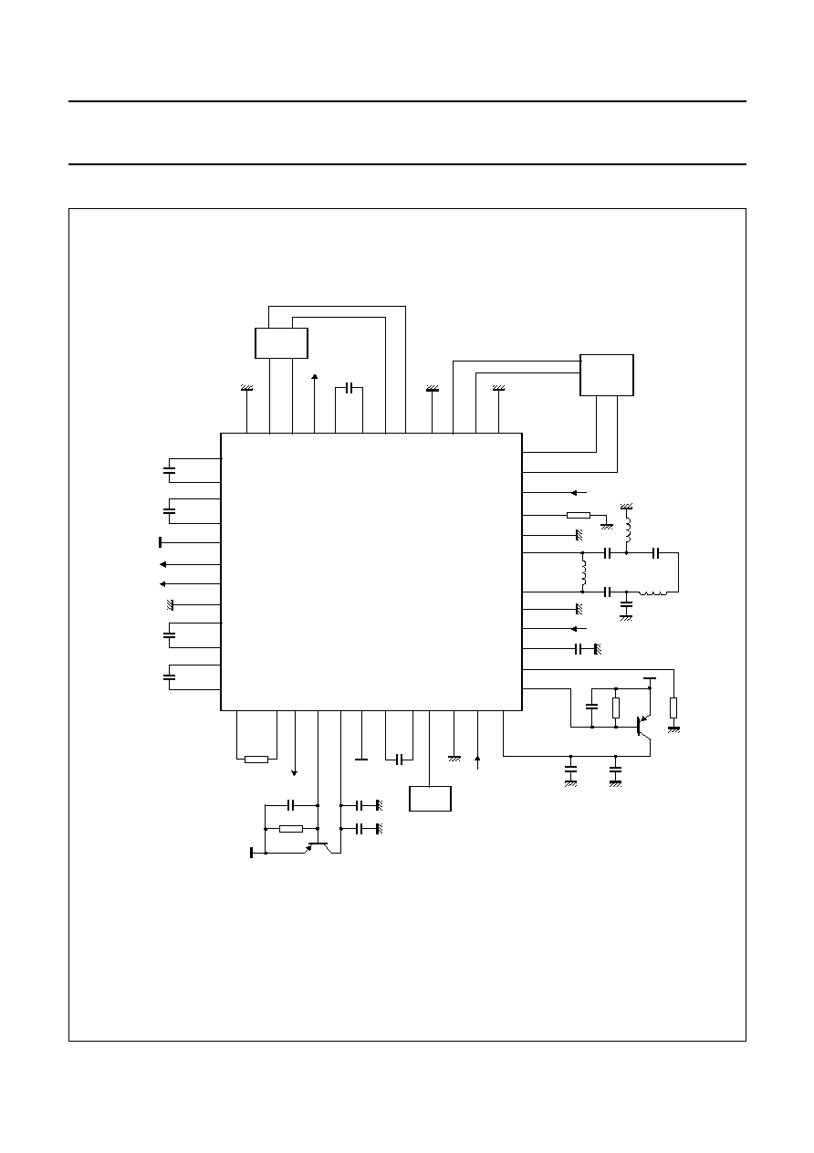
Fig.3 Demonstration board diagram.
Electrical diagram of the UAA3500HL demonstration board for FLEX
TM
applications. All matching is to 50
for measurement purposes.
B+ = 1.4 V; B++ = 2.1 V.

2000 Jan 18
13
Philips Semiconductors
Preliminary specification
Pager receiver
UAA3500HL
PACKAGE OUTLINE
UNIT
A
max.
A
1
A
2
A
3
b
p
c
E
(1)
e
H
E
L
L
p
Z
y
w
v
REFERENCES
OUTLINE
VERSION
EUROPEAN
PROJECTION
ISSUE DATE
IEC
JEDEC
EIAJ
mm
1.60
0.20
0.05
1.45
1.35
0.25
0.27
0.17
0.18
0.12
7.1
6.9
0.5
9.15
8.85
0.95
0.55
7
0
o
o
0.12
0.1
0.2
1.0
DIMENSIONS (mm are the original dimensions)
Note
1. Plastic or metal protrusions of 0.25 mm maximum per side are not included.
0.75
0.45
SOT313-2
MS-026
97-08-01
99-12-27
D
(1)
(1)
(1)
7.1
6.9
H
D
9.15
8.85
E
Z
0.95
0.55
D
b
p
e
E
B
12
D
H
b
p
E
H
v
M
B
D
ZD
A
Z E
e
v
M
A
1
48
37
36
25
24
13
A
1
A
L
p
detail X
L
(A )
3
A
2
X
y
c
w
M
w
M
0
2.5
5 mm
scale
pin 1 index
LQFP48: plastic low profile quad flat package; 48 leads; body 7 x 7 x 1.4 mm
SOT313-2

2000 Jan 18
14
Philips Semiconductors
Preliminary specification
Pager receiver
UAA3500HL
SOLDERING
Introduction to soldering surface mount packages
This text gives a very brief insight to a complex technology.
A more in-depth account of soldering ICs can be found in
our
"Data Handbook IC26; Integrated Circuit Packages"
(document order number 9398 652 90011).
There is no soldering method that is ideal for all surface
mount IC packages. Wave soldering is not always suitable
for surface mount ICs, or for printed-circuit boards with
high population densities. In these situations reflow
soldering is often used.
Reflow soldering
Reflow soldering requires solder paste (a suspension of
fine solder particles, flux and binding agent) to be applied
to the printed-circuit board by screen printing, stencilling or
pressure-syringe dispensing before package placement.
Several methods exist for reflowing; for example,
infrared/convection heating in a conveyor type oven.
Throughput times (preheating, soldering and cooling) vary
between 100 and 200 seconds depending on heating
method.
Typical reflow peak temperatures range from
215 to 250
∞
C. The top-surface temperature of the
packages should preferable be kept below 230
∞
C.
Wave soldering
Conventional single wave soldering is not recommended
for surface mount devices (SMDs) or printed-circuit boards
with a high component density, as solder bridging and
non-wetting can present major problems.
To overcome these problems the double-wave soldering
method was specifically developed.
If wave soldering is used the following conditions must be
observed for optimal results:
∑
Use a double-wave soldering method comprising a
turbulent wave with high upward pressure followed by a
smooth laminar wave.
∑
For packages with leads on two sides and a pitch (e):
≠ larger than or equal to 1.27 mm, the footprint
longitudinal axis is preferred to be parallel to the
transport direction of the printed-circuit board;
≠ smaller than 1.27 mm, the footprint longitudinal axis
must be parallel to the transport direction of the
printed-circuit board.
The footprint must incorporate solder thieves at the
downstream end.
∑
For packages with leads on four sides, the footprint must
be placed at a 45
∞
angle to the transport direction of the
printed-circuit board. The footprint must incorporate
solder thieves downstream and at the side corners.
During placement and before soldering, the package must
be fixed with a droplet of adhesive. The adhesive can be
applied by screen printing, pin transfer or syringe
dispensing. The package can be soldered after the
adhesive is cured.
Typical dwell time is 4 seconds at 250
∞
C. A
mildly-activated flux will eliminate the need for removal of
corrosive residues in most applications.
Manual soldering
Fix the component by first soldering two
diagonally-opposite end leads. Use a low voltage (24 V or
less) soldering iron applied to the flat part of the lead.
Contact time must be limited to 10 seconds at up to
300
∞
C.
When using a dedicated tool, all other leads can be
soldered in one operation within 2 to 5 seconds between
270 and 320
∞
C.

2000 Jan 18
15
Philips Semiconductors
Preliminary specification
Pager receiver
UAA3500HL
Suitability of surface mount IC packages for wave and reflow soldering methods
Notes
1. All surface mount (SMD) packages are moisture sensitive. Depending upon the moisture content, the maximum
temperature (with respect to time) and body size of the package, there is a risk that internal or external package
cracks may occur due to vaporization of the moisture in them (the so called popcorn effect). For details, refer to the
Drypack information in the
"Data Handbook IC26; Integrated Circuit Packages; Section: Packing Methods".
2. These packages are not suitable for wave soldering as a solder joint between the printed-circuit board and heatsink
(at bottom version) can not be achieved, and as solder may stick to the heatsink (on top version).
3. If wave soldering is considered, then the package must be placed at a 45
∞
angle to the solder wave direction.
The package footprint must incorporate solder thieves downstream and at the side corners.
4. Wave soldering is only suitable for LQFP, TQFP and QFP packages with a pitch (e) equal to or larger than 0.8 mm;
it is definitely not suitable for packages with a pitch (e) equal to or smaller than 0.65 mm.
5. Wave soldering is only suitable for SSOP and TSSOP packages with a pitch (e) equal to or larger than 0.65 mm; it is
definitely not suitable for packages with a pitch (e) equal to or smaller than 0.5 mm.
DEFINITIONS
LIFE SUPPORT APPLICATIONS
These products are not designed for use in life support appliances, devices, or systems where malfunction of these
products can reasonably be expected to result in personal injury. Philips customers using or selling these products for
use in such applications do so at their own risk and agree to fully indemnify Philips for any damages resulting from such
improper use or sale.
PACKAGE
SOLDERING METHOD
WAVE
REFLOW
(1)
BGA, SQFP
not suitable
suitable
HLQFP, HSQFP, HSOP, HTSSOP, SMS
not suitable
(2)
suitable
PLCC
(3)
, SO, SOJ
suitable
suitable
LQFP, QFP, TQFP
not recommended
(3)(4)
suitable
SSOP, TSSOP, VSO
not recommended
(5)
suitable
Data sheet status
Objective specification
This data sheet contains target or goal specifications for product development.
Preliminary specification
This data sheet contains preliminary data; supplementary data may be published later.
Product specification
This data sheet contains final product specifications.
Limiting values
Limiting values given are in accordance with the Absolute Maximum Rating System (IEC 134). Stress above one or
more of the limiting values may cause permanent damage to the device. These are stress ratings only and operation
of the device at these or at any other conditions above those given in the Characteristics sections of the specification
is not implied. Exposure to limiting values for extended periods may affect device reliability.
Application information
Where application information is given, it is advisory and does not form part of the specification.

© Philips Electronics N.V.
SCA
All rights are reserved. Reproduction in whole or in part is prohibited without the prior written consent of the copyright owner.
The information presented in this document does not form part of any quotation or contract, is believed to be accurate and reliable and may be changed
without notice. No liability will be accepted by the publisher for any consequence of its use. Publication thereof does not convey nor imply any license
under patent- or other industrial or intellectual property rights.
Internet: http://www.semiconductors.philips.com
2000
69
Philips Semiconductors ≠ a worldwide company
For all other countries apply to: Philips Semiconductors,
International Marketing & Sales Communications, Building BE-p, P.O. Box 218,
5600 MD EINDHOVEN, The Netherlands, Fax. +31 40 27 24825
Argentina: see South America
Australia: 3 Figtree Drive, HOMEBUSH, NSW 2140,
Tel. +61 2 9704 8141, Fax. +61 2 9704 8139
Austria: Computerstr. 6, A-1101 WIEN, P.O. Box 213,
Tel. +43 1 60 101 1248, Fax. +43 1 60 101 1210
Belarus: Hotel Minsk Business Center, Bld. 3, r. 1211, Volodarski Str. 6,
220050 MINSK, Tel. +375 172 20 0733, Fax. +375 172 20 0773
Belgium: see The Netherlands
Brazil: see South America
Bulgaria: Philips Bulgaria Ltd., Energoproject, 15th floor,
51 James Bourchier Blvd., 1407 SOFIA,
Tel. +359 2 68 9211, Fax. +359 2 68 9102
Canada: PHILIPS SEMICONDUCTORS/COMPONENTS,
Tel. +1 800 234 7381, Fax. +1 800 943 0087
China/Hong Kong: 501 Hong Kong Industrial Technology Centre,
72 Tat Chee Avenue, Kowloon Tong, HONG KONG,
Tel. +852 2319 7888, Fax. +852 2319 7700
Colombia: see South America
Czech Republic: see Austria
Denmark: Sydhavnsgade 23, 1780 COPENHAGEN V,
Tel. +45 33 29 3333, Fax. +45 33 29 3905
Finland: Sinikalliontie 3, FIN-02630 ESPOO,
Tel. +358 9 615 800, Fax. +358 9 6158 0920
France: 51 Rue Carnot, BP317, 92156 SURESNES Cedex,
Tel. +33 1 4099 6161, Fax. +33 1 4099 6427
Germany: Hammerbrookstraþe 69, D-20097 HAMBURG,
Tel. +49 40 2353 60, Fax. +49 40 2353 6300
Hungary: see Austria
India: Philips INDIA Ltd, Band Box Building, 2nd floor,
254-D, Dr. Annie Besant Road, Worli, MUMBAI 400 025,
Tel. +91 22 493 8541, Fax. +91 22 493 0966
Indonesia: PT Philips Development Corporation, Semiconductors Division,
Gedung Philips, Jl. Buncit Raya Kav.99-100, JAKARTA 12510,
Tel. +62 21 794 0040 ext. 2501, Fax. +62 21 794 0080
Ireland: Newstead, Clonskeagh, DUBLIN 14,
Tel. +353 1 7640 000, Fax. +353 1 7640 200
Israel: RAPAC Electronics, 7 Kehilat Saloniki St, PO Box 18053,
TEL AVIV 61180, Tel. +972 3 645 0444, Fax. +972 3 649 1007
Italy: PHILIPS SEMICONDUCTORS, Via Casati, 23 - 20052 MONZA (MI),
Tel. +39 039 203 6838, Fax +39 039 203 6800
Japan: Philips Bldg 13-37, Kohnan 2-chome, Minato-ku,
TOKYO 108-8507, Tel. +81 3 3740 5130, Fax. +81 3 3740 5057
Korea: Philips House, 260-199 Itaewon-dong, Yongsan-ku, SEOUL,
Tel. +82 2 709 1412, Fax. +82 2 709 1415
Malaysia: No. 76 Jalan Universiti, 46200 PETALING JAYA, SELANGOR,
Tel. +60 3 750 5214, Fax. +60 3 757 4880
Mexico: 5900 Gateway East, Suite 200, EL PASO, TEXAS 79905,
Tel. +9-5 800 234 7381, Fax +9-5 800 943 0087
Middle East: see Italy
Netherlands: Postbus 90050, 5600 PB EINDHOVEN, Bldg. VB,
Tel. +31 40 27 82785, Fax. +31 40 27 88399
New Zealand: 2 Wagener Place, C.P.O. Box 1041, AUCKLAND,
Tel. +64 9 849 4160, Fax. +64 9 849 7811
Norway: Box 1, Manglerud 0612, OSLO,
Tel. +47 22 74 8000, Fax. +47 22 74 8341
Pakistan: see Singapore
Philippines: Philips Semiconductors Philippines Inc.,
106 Valero St. Salcedo Village, P.O. Box 2108 MCC, MAKATI,
Metro MANILA, Tel. +63 2 816 6380, Fax. +63 2 817 3474
Poland: Al.Jerozolimskie 195 B, 02-222 WARSAW,
Tel. +48 22 5710 000, Fax. +48 22 5710 001
Portugal: see Spain
Romania: see Italy
Russia: Philips Russia, Ul. Usatcheva 35A, 119048 MOSCOW,
Tel. +7 095 755 6918, Fax. +7 095 755 6919
Singapore: Lorong 1, Toa Payoh, SINGAPORE 319762,
Tel. +65 350 2538, Fax. +65 251 6500
Slovakia: see Austria
Slovenia: see Italy
South Africa: S.A. PHILIPS Pty Ltd., 195-215 Main Road Martindale,
2092 JOHANNESBURG, P.O. Box 58088 Newville 2114,
Tel. +27 11 471 5401, Fax. +27 11 471 5398
South America: Al. Vicente Pinzon, 173, 6th floor,
04547-130 S√O PAULO, SP, Brazil,
Tel. +55 11 821 2333, Fax. +55 11 821 2382
Spain: Balmes 22, 08007 BARCELONA,
Tel. +34 93 301 6312, Fax. +34 93 301 4107
Sweden: Kottbygatan 7, Akalla, S-16485 STOCKHOLM,
Tel. +46 8 5985 2000, Fax. +46 8 5985 2745
Switzerland: Allmendstrasse 140, CH-8027 ZÐRICH,
Tel. +41 1 488 2741 Fax. +41 1 488 3263
Taiwan: Philips Semiconductors, 6F, No. 96, Chien Kuo N. Rd., Sec. 1,
TAIPEI, Taiwan Tel. +886 2 2134 2886, Fax. +886 2 2134 2874
Thailand: PHILIPS ELECTRONICS (THAILAND) Ltd.,
209/2 Sanpavuth-Bangna Road Prakanong, BANGKOK 10260,
Tel. +66 2 745 4090, Fax. +66 2 398 0793
Turkey: Yukari Dudullu, Org. San. Blg., 2.Cad. Nr. 28 81260 Umraniye,
ISTANBUL, Tel. +90 216 522 1500, Fax. +90 216 522 1813
Ukraine: PHILIPS UKRAINE, 4 Patrice Lumumba str., Building B, Floor 7,
252042 KIEV, Tel. +380 44 264 2776, Fax. +380 44 268 0461
United Kingdom: Philips Semiconductors Ltd., 276 Bath Road, Hayes,
MIDDLESEX UB3 5BX, Tel. +44 208 730 5000, Fax. +44 208 754 8421
United States: 811 East Arques Avenue, SUNNYVALE, CA 94088-3409,
Tel. +1 800 234 7381, Fax. +1 800 943 0087
Uruguay: see South America
Vietnam: see Singapore
Yugoslavia: PHILIPS, Trg N. Pasica 5/v, 11000 BEOGRAD,
Tel. +381 11 3341 299, Fax.+381 11 3342 553
Printed in The Netherlands
465008/02/pp
16
Date of release:
2000 Jan 18
Document order number:
9397 750 06478