2000 Feb 17
2
Philips Semiconductors
Objective specification
Low power GSM/DCS/PCS multi-band transceiver
UAA3535HL
FEATURES
∑
Multi-band application for GSM, DCS and PCS cellular
phone systems
∑
Low noise and wide dynamic range low IF receiver
∑
More than 35 dB on-chip image rejection in receive
mode
∑
More than 64 dB gain control range in receive mode
∑
Integrated channel filter
∑
Integrated TX low-pass filter
∑
High precision I/Q modulator
∑
Multi-band TX modulation loop architecture including
offset mixer and phase-frequency detector
∑
Dual PLL with on-chip fully integrated IF VCO
∑
Fully differential design minimizing crosstalk and
spurious signals
∑
Functional down to 2.4 V and up to 3.6 V
∑
3-wire serial bus interface
∑
LQFP48 package.
APPLICATIONS
∑
GSM 900 MHz, DCS 1800 MHz and PCS 1900 MHz
hand-held transceivers.
GENERAL DESCRIPTION
The UAA3535HL is intended for Global Systems for
Mobile communication (GSM), Digital Cellular
communication Systems (DCS) and Personal
Communication Services (PCS). The circuit integrates the
receiver and most of the transmitter section of hand-held
transceivers for these applications.
The receiver consists of two sections. The first section is
the RF receiver front-end, which amplifies the GSM, DCS
or PCS aerial signal, then converts the chosen channel
down to a low Intermediate Frequency (IF) of 100 kHz,
and also provides more than 35 dB image suppression.
Some selectivity is provided at this stage by an on-chip
low-pass filter and channel selectivity is provided by a high
performance integrated band-pass filter.
The second section is the IF section, which further
amplifies the chosen channel and performs gain control to
adjust the output level to the desired value. The IF gain
can be varied over more than 64 dB gain range.
The transmitter also consists of two sections. The first is a
high precision I/Q modulator which converts the baseband
modulation up to the transmit IF. The second is a
modulation loop architecture which converts the signal
to RF.
The Local Oscillator (LO) signals are provided by an
on-chip Voltage Controlled Oscillator (VCO) for operation
of the IF section and are provided externally for operation
of the RF section. The frequencies of the RF and IF VCOs
are set by internal PLL circuits, which are programmable
via a 3-wire serial bus. Comparison frequencies are
200 kHz (100 kHz step programmability) and 13 MHz for
the RF and IF PLL respectively, and are derived from a
13 MHz reference signal which has to be supplied
externally. The quadrature-phase RF LO signals required
for I/Q mixers in reception are generated internally.
The quadrature LO signals required for operation of the
I/Q modulator are generated inside the IF VCO.
The circuit can be powered-up into one of three different
modes: RX, TX or SYN mode, depending on the logic
state of pins RXON, TXON and SYNON, respectively. It is
also possible to set the IC in one of these modes by
software, using the 3-wire bus serial programming.
In RX (TX) mode, all sections required for receive
(transmit) are turned on. The SYN mode is used to
power-up the synthesizers prior to the RX or TX mode.
In the SYN mode, some internal LO buffers are also
powered-up in such a way that VCO pulling is minimized
when switching on the receiver or the transmitter.
Additional band selection is done using the 3-wire bus
serial programming, allowing the required enabling of the
Low Noise Amplifiers (LNAs) and charge pumps current
programming.
ORDERING INFORMATION
TYPE
NUMBER
PACKAGE
NAME
DESCRIPTION
VERSION
UAA3535HL
LQFP48
plastic low profile quad flat package; 48 leads; body 7
◊
7
◊
1.4 mm
SOT313-2
2000 Feb 17
4
Philips Semiconductors
Objective specification
Low power GSM/DCS/PCS multi-band transceiver
UAA3535HL
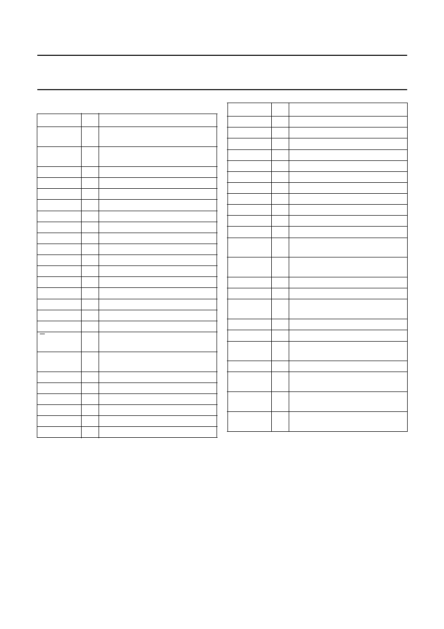
PINNING
SYMBOL
PIN
DESCRIPTION
TXCPO
1
transmit modulation loop GSM
charge pump output
V
CC(TXCP)
2
transmit modulation loop charge
pump supply voltage
TXIFA
3
transmit IF test pin
IFGND1
4
IF ground 1
TSTO
5
test mode output
V
CC1(IF)
6
IF supply voltage 1
IA
7
I path A baseband input/output
IB
8
I path B baseband input/output
QA
9
Q path A baseband input/output
QB
10
Q path B baseband input/output
RXON
11
RX mode control input
TXON
12
TX mode control input
IFTUNE
13
transmit IF VCO tune input
V
CC2(IF)
14
IF supply voltage 2
IFGND2
15
IF ground 2
DATA
16
3-wire bus data input
CLK
17
3-wire bus clock input
E
18
3-wire bus enable control input
(active LOW)
V
CC(IFCP)
19
transmit IF charge pump supply
voltage
IFCPO
20
transmit IF charge pump output
IFCPGND
21
transmit IF charge pump ground
REFIN
22
synthesizers reference input
RFCPGND
23
RF charge pump ground
RFCPO
24
RF charge pump output
SYNON
25
SYN mode control input
V
CC(RFCP)
26
RF charge pump supply voltage
V
CC(SYN)
27
synthesizers supply voltage
SYNGND
28
synthesizers ground
RFLOGND
29
RF LO ground
RFLOIA
30
RF LO input A
RFLOIB
31
RF LO input B
V
CC(RFLO)
32
RF LO supply voltage
IFCQB
33
RX IF Q test pin B
IFCQA
34
RX IF Q test pin A
IFCIB
35
RX IF I test pin B
IFCIA
36
RX IF I test pin A
V
CC(RF)
37
RF front-end and transmit
modulation loop supply voltage
RFGND1
38
RF front-end and transmit
modulation loop ground 1
GSMIA
39
receiver GSM RF input A
GSMIB
40
receiver GSM RF input B
RFGND2
41
RF front-end and transmit
modulation loop ground 2
DCSPCSIA
42
receiver DCS/PCS RF input A
DCSPCSIB
43
receiver DCS/PCS RF input B
RFGND3
44
RF front-end and transmit
modulation loop ground 3
TXRFI
45
input from RF transmit VCOs
RFGND4
46
RF front-end and transmit
modulation loop ground 4
EXTRES
47
reference resistor for transmit
modulation loop
TXCPGND
48
transmit modulation loop charge
pump ground
SYMBOL
PIN
DESCRIPTION
2000 Feb 17
5
Philips Semiconductors
Objective specification
Low power GSM/DCS/PCS multi-band transceiver
UAA3535HL
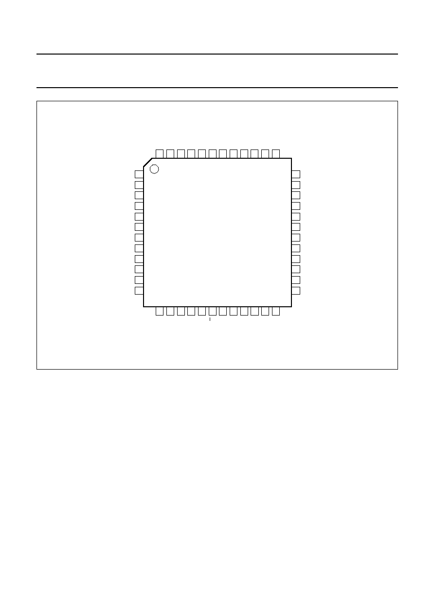
handbook, full pagewidth
1
2
3
4
5
6
7
8
9
10
11
36
35
34
33
32
31
30
29
28
27
26
13
14
15
16
17
18
19
20
21
22
23
48
47
46
45
44
43
42
41
40
39
38
12
24
37
25
UAA3535HL
FCA068
IFCIA
IFCIB
IFCQA
IFCQB
RFLOIB
RFLOIA
RFLOGND
SYNGND
VCC(SYN)
VCC(RFCP)
SYNON
VCC(RFLO)
EXTRES
RFGND4
TXRFI
RFGND3
DCSPCSIB
DCSPCSIA
GSMIB
GSMIA
RFGND1
V
CC(RF)
TXCPGND
RFGND2
TXCPO
VCC(TXCP)
TXIFA
IFGND1
TSTO
VCC1(IF)
IB
QA
RXON
TXON
IA
QB
V
CC2(IF)
IFGND2
DATA
V
CC(IFCP)
IFCPO
REFIN
RFCPGND
RFCPO
IFTUNE
IFCPGND
CLK
E
Fig.2 Pin configuration.
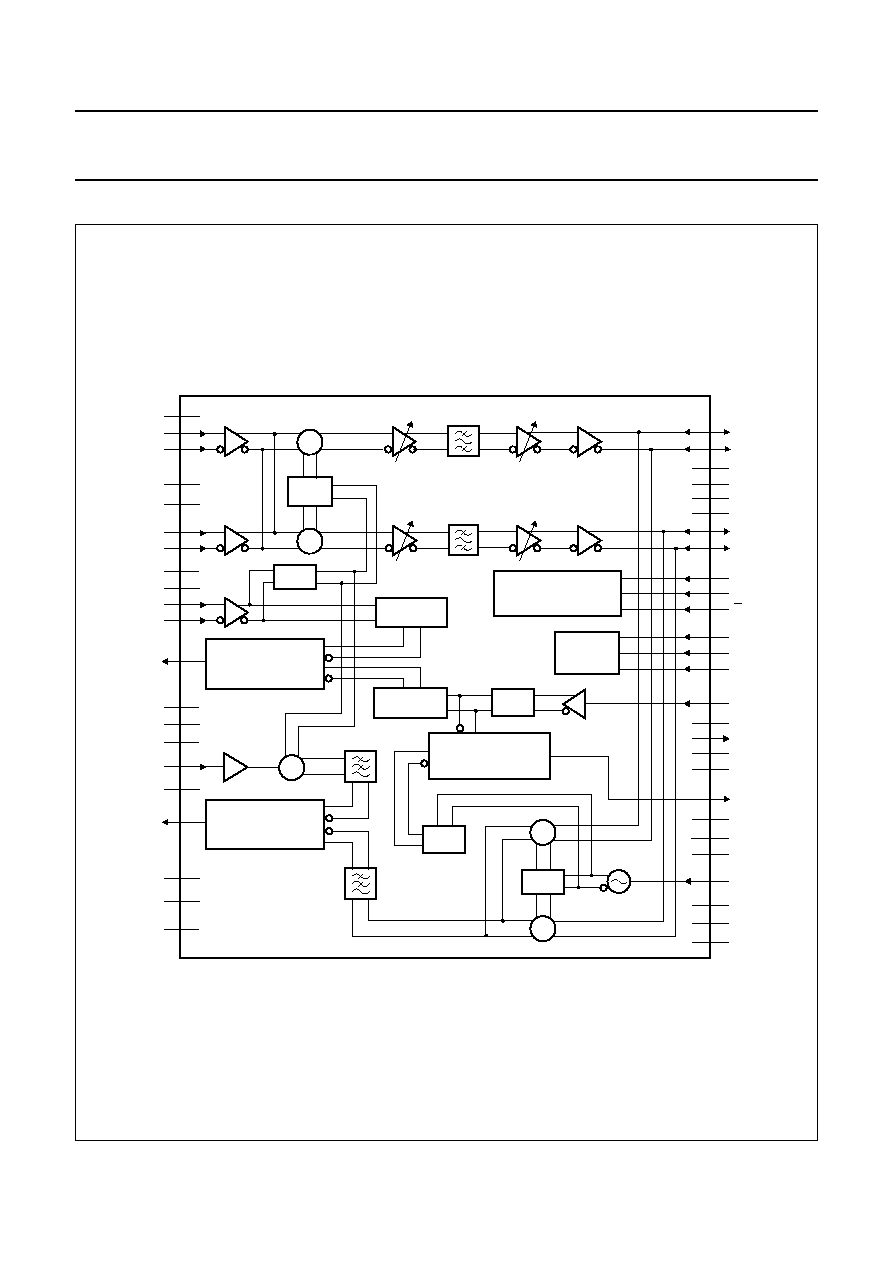
FUNCTIONAL DESCRIPTION
RF receiver
The receiver front-end converts the aerial RF signal from
EGSM (Extended GSM; 925 to 960 MHz), DCS
(1805 to 1880 MHz) or PCS (1930 to 1990 MHz) bands
down to an IF signal of 100 kHz. The first stages are
symmetrical LNAs that are matched to 50
using external
baluns. The LNAs are followed by an I/Q down-mixer.
The I/Q down-mixer consists of two mixers in parallel but
driven by quadrature out of phase LO signals.
The In-phase (I) and Quadrature- phase (Q) IF signals are
then low-pass filtered to provide protection from high
frequency offset interferers. The IF I and Q signals are
then fed into the channel filter.
Channel filter and AGC
The front-end IF I and Q outputs are first applied to an
amplifier circuit with provision for three 8 dB gain step
adjustment possibilities and then to an integrated
band-pass channel filter. The filter is a fifth-order
band-pass filter centred around 100 with 220 kHz
bandwidth. After filtering the IF I and Q signals are further
amplified with provision for eleven 4 dB gain steps and
DC offset compensation.
I/Q modulator
I and Q baseband signals are applied to the I/Q modulator
where the modulation spectrum is shifted up to the
transmit IF frequency. For low harmonic distortion, low
carrier leakage and high image rejection, the phase error
must be kept as small as possible. The IF output of the
modulator is fed to an integrated low-pass filter where
unwanted spurious signals are suppressed, prior to being
fed to the phase detector.