 | –≠–ª–µ–∫—Ç—Ä–æ–Ω–Ω—ã–π –∫–æ–º–ø–æ–Ω–µ–Ω—Ç: UAA3545HL | –°–∫–∞—á–∞—Ç—å:  PDF PDF  ZIP ZIP |
Document Outline
- FEATURES
- APPLICATIONS
- GENERAL DESCRIPTION
- ORDERING INFORMATION
- QUICK REFERENCE DATA
- BLOCK DIAGRAM
- PINNING
- FUNCTIONAL DESCRIPTION
- LIMITING VALUES
- HANDLING
- LATCH-UP
- THERMAL CHARACTERISTICS
- CHARACTERISTICS
- PACKAGE OUTLINE
- SOLDERING
- DATA SHEET STATUS
- DEFINITIONS
- DISCLAIMERS

DATA SHEET
Product specification
File under Integrated Circuits, IC17
2001 Sep 06
INTEGRATED CIRCUITS
UAA3545
Fully integrated DECT transceiver

2001 Sep 06
2
Philips Semiconductors
Product specification
Fully integrated DECT transceiver
UAA3545
FEATURES
∑
Economical solution for a radio in DECT cordless
telephones
∑
Integrated low phase noise VCO with no production
tuning required
∑
Fully integrated receiver with high sensitivity
∑
Dedicated DECT PLL synthesizer
∑
3 dBm output preamplifier with an integrated switch
∑
3-line serial interface bus
∑
Low current consumption from a 3.2 V supply
∑
Compatible with Philips Semiconductors baseband
chips (PCD509xx and PCD80xxx)
∑
Reduced number of control signals.
APPLICATIONS
∑
DECT cordless telephones: 1880 to 1930 MHz.
GENERAL DESCRIPTION
The UAA3545 BiCMOS device is a low power, highly
integrated circuit, for Digital Enhanced Cordless
Telecommunication (DECT) applications.
It features a fully integrated receiver, from antenna filter
output to the demodulated data output, a fully integrated
VCO, a synthesizer to implement a phase-locked loop for
DECT channel frequencies and a TX preamplifier to drive
the external transmit power amplifier (CGY20xx series or
UAA359x series of Philips integrated circuits).
The synthesizer's main divider is driven by the prescaler
output in the range of 1880 to 1930 MHz and is
programmed via a 3-wire serial bus. The reference divider
ratio is programmable to 4, 8, 12 or 16. Outputs of the
main and reference dividers drive a phase comparator
where a charge pump produces phase error current pulses
for integration in an external loop filter (only a passive loop
filter is necessary). The charge-pump current is set to
4 mA for fast switching.
The VCO is powered from an internally regulated voltage
source and includes integrated variable capacitance
diodes and integrated coils. Its tuning range is guaranteed.
The VCO and the synthesizer are switched-on one slot
before the active slot to lock the VCO to the required
channel frequency. Immediately before the active slot, the
synthesizer is switched-off to allow open loop modulation
of the VCO during transmission. When opening the loop,
frequency pulling (due to switching-off the synthesizer)
can be maintained within the DECT specification.
The device is designed to operate from a 3.2 V nominal
supply. Separate power and ground pins are provided for
the different sections of the circuit. Ground leads should be
short-circuited externally to prevent large currents flowing
across the die and causing damage. All V
CC
supplies
(V
CC(REG)
, V
CC(SYN)
, V
CC(RX)
and V
CC(TX)
) must be at the
same potential (V
CC
).
ORDERING INFORMATION
TYPE
NUMBER
PACKAGE
NAME
DESCRIPTION
VERSION
UAA3545HL
LQFP32
plastic low profile quad flat package; 32 leads; body 5
◊
5
◊
1.4 mm
SOT401-1

2001 Sep 06
3
Philips Semiconductors
Product specification
Fully integrated DECT transceiver
UAA3545
QUICK REFERENCE DATA
V
CC
= 3.2 V; T
amb
= 25
∞
C; characteristics with a typical value only are not tested; unless otherwise specified.
SYMBOL
PARAMETER
CONDITIONS
MIN.
TYP.
MAX.
UNIT
V
CC(syn)
,
V
CC(reg)
,
V
CC(RX)
,
V
CC(TX)
supply voltage
All V
CC
supplies
must be at the
same potential
(V
CC
)
3.0
3.2
3.6
V
I
CC(SYN)
synthesizer supply current
synthesizer ON
-
5
7
mA
I
CC(REG)
VCO, buffer and prescaler regulator
supply current
VCO ON
-
14
17
mA
I
CC(RX)
receiver supply current
-
36
44
mA
I
CC(TX)
transmit preamplifier supply current
-
12
15
mA
I
CC(pd)
total supply current in Power-down mode
-
10
100
µ
A
f
o(RF)
RF output frequency
1880
-
1930
MHz
f
(i)XTAL
crystal reference input frequency
-
3.456,
6.912,
10.368 or
13.824
-
MHz
f
PC
phase comparator frequency
-
864
-
kHz
T
amb
ambient temperature
-
10
-
+60
∞
C

2001 Sep 06
4
Philips Semiconductors
Product specification
Fully integrated DECT transceiver
UAA3545
BLOCK DIAGRAM
handbook, full pagewidth
MGW108
◊
LNA
AMP
RFA
RFB
TXA
TXB
R_ON
VCO_ON
CP/VCOtune
RDATAP
SLCCTR
DATAM
VMOD
VCC(SYN)
VCC(REG)
VCC(RX)
RSSI
12
16
VCC(TX)
22
TXGND
UAA3545
19
RXGND
13
SLICER
15
14
20
21
17
1
S_CLK
8
S_EN
6
S_DATA
4
5
TEST2
29
TEST3
XTAL
18
DIVGND
23
VREGDIV
24
3
TEST1
28
32
25
7
11
9
SYNGND
10
REGGND
30
VCOGND
27
VREGO
31
VREGI
26
2
CONTROL
LOGIC
SYNTHESIZER
PRESCALER
VCO
REGULATOR
DEMODULATOR
LIMITER
SLIC = 1
SLIC = 1
SLIC = 1
0
0
0
1 k
(1)
Fig.1 Block diagram.
(1) SLCCTR `switches' shown in position SLCCTR = LOW.

2001 Sep 06
5
Philips Semiconductors
Product specification
Fully integrated DECT transceiver
UAA3545
PINNING
Notes
1. Corresponds to the S_PWR of the baseband chip (see Section "Operating modes" for more details).
2. Corresponds to the REF_CLK of the baseband chip.
3. See Section "Operating modes" for more details.
SYMBOL
PIN
DESCRIPTION
VCO_ON
1
VCO section power-on control; note 1
V
CC(REG)
2
regulator positive supply voltage
V
CC(SYN)
3
synthesizer positive supply voltage
S_DATA
4
3-wire bus data signal input
XTAL
5
reference frequency input; note 2
S_EN
6
3-wire bus enable signal input
RDATAP
7
demodulator output voltage
S_CLK
8
3-wire bus clock signal input
DATAM
9
switched demodulator output voltage
SYNGND
10
synthesizer ground
SLCCTR
11
DATAM switch control signal (see Fig.1)
RSSI
12
received signal strength intensity voltage output
RXGND
13
receiver ground
RFB
14
received signal input B
RFA
15
received signal input A
V
CC(RX)
16
receiver positive supply voltage
R_ON
17
receiver power-on control; note 3
TEST3
18
TEST input 3 (must be connected to GND)
TXGND
19
transmitter ground
TXA
20
transmit amplifier output A
TXB
21
transmit amplifier output B
V
CC(TX)
22
transmitter positive supply voltage
DIVGND
23
divider ground
VREGDIV
24
divider regulated supply voltage
V
MOD
25
VCO analog modulation voltage input
VREGI
26
VCO regulated voltage input
VCOGND
27
VCO ground
TEST1
28
TEST input 1 (must not be connected)
TEST2
29
TEST input 2 (must not be connected)
REGGND
30
regulator ground
VREGO
31
VCO section regulated voltage output
CP/VCO
tune
32
charge-pump output/VCO tuning input
2001 Sep 06
6
Philips Semiconductors
Product specification
Fully integrated DECT transceiver
UAA3545
handbook, full pagewidth
1
2
3
4
5
6
7
8
24
23
22
21
20
19
18
17
9
10
11
12
13
14
15
16
32
31
30
29
28
27
26
25
UAA3545HL
FCA242
CP/
VCO
tune
VREGO
REGGND
TEST2
TEST1
VCOGND
VREGI
V
MOD
DATAM
SYNGND
SLCCTR
RSSI
RXGND
RFB
RFA
V
CC(RX)
VCO_ON
VCC(REG)
VCC(SYN)
S_DATA
XTAL
S_EN
RDATAP
S_CLK
VREGDIV
DIVGND
VCC(TX)
TXB
TXA
TXGND
TEST3
R_ON
Fig.2 Pin configuration.

2001 Sep 06
7
Philips Semiconductors
Product specification
Fully integrated DECT transceiver
UAA3545
FUNCTIONAL DESCRIPTION
Transmit chain
VCO
AND PRESCALER
The fully integrated VCO operates at a multiple of the
DECT frequency. It is supplied by an on-chip voltage
regulator to minimize frequency disturbances due to
supply voltage variations. The VCO signal is fed into a
prescaler. A large difference between transmitted and
VCO frequencies reduces transmitter-oscillator coupling
problems.
The output of the prescaler drives the synthesizer main
divider. The divider output can also be switched to either
the TX preamplifier or the RX LO output buffer. The high
isolation obtained from the prescaler ensures very small
frequency changes when turning-on the TX preamplifier or
the RX section. In TX mode, the oscillator can be
modulated directly with GFSK-filtered data at pin V
MOD
.
TX
PREAMPLIFIER
The TX preamplifier amplifies the RF signal to a level of
3 dBm (typical) which is suitable for use with Philips
Semiconductors DECT power amplifiers.
Synthesizer
M
AIN DIVIDER
The main divider is clocked by the RF signal from the
prescaler at frequencies from 1880 to 1930 MHz. Any
main divider ratio from 2176 to 2303 inclusive can be
programmed.
R
EFERENCE DIVIDER
The reference divider is clocked by the signal at pin XTAL.
The circuit operates with levels from 1.2 to 1.8 V (p-p) at a
frequency of 3.456 MHz. By programming the `REFD' bits
of the serial input register (see Table 1) the reference
frequency can be set for 6.912, 10.368 or 13.864 MHz.
P
HASE COMPARATOR
The phase comparator is driven by the output of the main
and reference dividers. It produces current pulses at
pin CP/VCO
tune
, the pulse duration being the difference in
arrival time of current pulse edges from the two dividers.
If the main divider edge arrives first, pin CP sinks current.
If the reference divider edge arrives first, pin CP sources
current. The DC value of the charge-pump current is
defined by an internal resistor. Additional circuitry is
included to ensure the gain of the phase detector remains
linear even for small phase errors.
Serial programming bus
A simple 3-line unidirectional serial bus is used to
program the circuit. The three lines are data (S_DATA),
serial clock (S_CLK) and serial bus enable (S_EN). Data
sent to the device are loaded in bursts framed by S_EN.
Programming clock edges and their appropriate data bits
are ignored until S_EN goes active (LOW). The
programmed information is read directly by the main
divider when S_EN returns to HIGH. S_DATA and S_EN
change value on the falling edge of S_CLK.
During synthesizer operation, S_EN should be held
HIGH. Only the last 24 bits clocked into the device are
retained within the serial register. Additional leading bits
are ignored and no check is made on the number of clock
pulses. The data format is shown in Table 1. The first bit
entered is b23, the last bit is b0. For the main divider ratio,
the first bit (b5) is the Most Significant Bit (MSB).
The serial bus enable (S_EN) must be LOW to capture
new programming data and must be HIGH to switch on the
synthesizer.

2001 Sep 06
8
Philips Semiconductors
Product specification
Fully integrated DECT transceiver
UAA3545
Receiver
The receiver is a fully integrated RF + IF strip and
demodulator for DECT. It provides all the required channel
filtering over the DECT band and generates analog RSSI
and a switched output for Philips Semiconductors
baseband chip. Very few off-chip components are required
and all of these can be placed without trimming. The chip
is designed to operate with a power supply voltage that
can fall to 3.0 V. The input is the RF antenna signal
derived from the band filter or the antenna switch. The
outputs are the RSSI voltage, representing the
instantaneous signal strength and two HIGH-level
demodulator output signals RDATAP and DATAM, the
latter being switched by SLCCTR to generate the external
slicer threshold. During the blind slot, while the PLL is
settling, an internal voltage source is activated to
precharge the external capacitor (connected to
pin DATAM) to a voltage close to the required slicer
threshold.
Operating modes
The operating modes available are:
∑
Normal mode (see Fig.3)
∑
Reduced signal mode (see Fig.4)
∑
Advanced signal mode (see Fig.5).
Selection of an operating mode is achieved via the serial
interface register (see Table 3).
N
ORMAL MODE
(
MODE
1)
In the normal mode, the synthesizer is ON when
S_EN = HIGH and VCO_ON = HIGH, and OFF when
S_EN = LOW. When turned ON, the dividers and phase
detector are synchronized to avoid a random initial phase
error. When turned OFF, the phase detector is
synchronized with the dividers to avoid interrupting a
charge-pump pulse. This feature requires a signal to be
present for a few microseconds on the XTAL pin after
S_EN goes LOW.
The VCO is ON when the input signal VCO_ON is HIGH.
The polarity of VCO_ON is chosen for compatibility with
output S_PWR of the baseband chip. When the VCO is
turned ON, it takes 50
µ
s (typical) to reach its steady state.
The TX preamplifier is ON when bit `TRX' is programmed
to `0' and VCO_ON is HIGH. When the TX preamplifier is
turned ON, it takes typically 10
µ
s to be ready. The
receiver is turned ON when R_ON = HIGH and
VCO_ON = HIGH.
R
EDUCED SIGNAL MODE
(
MODE
2)
In the reduced signal mode, the parallel control signals are
replaced by serial bus programming. To select this mode,
the bit `NEW' of the internal register must be set to `1' and
the bit `SPWR' must be reset to `0', timing is then
controlled by the S_EN signal.
After the register programming, the S_EN rising edge
programs the PLL, closes the loop, powers-on the VCO
and, if the `TRX' bit = 0, turns ON the TX preamplifier.
On the falling edge of the first S_EN pulse, the loop is
opened (unless the bit `PLL' is set to 1) and the receiver
switches ON if the `TRX' bit = 1. A second pulse on S_EN
is required at the end of the wanted slot to power-down the
application.
The R_ON pin becomes an output in this mode, drives the
RX PIN diode and corresponds to the internal power-on
signal of the receiver.
A
DVANCED SIGNAL MODE
(
MODE
3)
In the advanced signal mode, the parallel control signals
are partly replaced by serial bus programming. To select
this mode, the bit `NEW' and the bit `SPWR' of the internal
register must be set to `1'. The S_EN signal will then
control the UAA3545 timing (except for timing of a general
power-down as this is controlled by the VCO_ON input).
The VCO_ON signal should rise at the beginning of the
previous slot. After the serial bus has been programmed,
the S_EN rising edge programs the PLL, closes the loop
and, if the `TRX' bit = 0, turns ON the TX preamplifier.
On the falling edge of the first S_EN pulse, the loop is
opened (unless the `PLL' bit is set to 1) and the RX section
switches ON if bit `TRX' = 1. At the end of the wanted slot,
the VCO_ON goes LOW to power-down the whole IC.
In fact, the second pulse of the S_EN signal in mode 2 is
now replaced by the signal VCO_ON.
The R_ON pin becomes an output in this mode, drives the
RX PIN diode and corresponds to the internal power-on
signal of the receiver.

2001 Sep 06
9
Philips Semiconductors
Product specification
Fully integrated DECT transceiver
UAA3545
Programming
Table 1
Serial interface register
Notes
1. Bit b5 is the MSB of the main divider coefficient; this comprises bits b5, b4, b3, b2, b1, b0 and b6 (TRX).
2. Test bits b23, b22, b21, b20, b16, b15, b14, b13, b12, b11, b10 must always be programmed to 0.
3. Bit `SLIC' = 1 forces the internal slicer on. In this mode, pin DATAM is connected to an external capacitor. Together
with an internal 1 k
resistor, it defines the low pass time constant for the slicer threshold voltage. When the
bit `SLIC' = 0, the pin RDATAP is connected directly to the demodulator output and delivers an analog signal.
Pin DATAM also reflects the demodulator voltage without the internal 1 k
resistor when the SLCCTR pin is HIGH.
4. REFD sets the reference divider ratio to 4, 8, 12 or 16 (corresponding respectively to a reference input frequency of
3.456, 6.912, 10.368 or 13.824 MHz) (see Table 4).
5. Bits `NEW', and `SPWR' select the operating mode (see Table 3).
6. Bit `PLL' = 1 forces the PLL to remain on when the VCO is on.
7. The main divider ratio is equal to 2176 + the programmed value (see Table 2).
Table 2
Main divider programming
Table 3
Operating mode selection
Table 4
Reference divider ratio programming
REGISTER BIT ALLOCATION
first in
last in
b23 to b20
b19
b18, b17
b16 to b10
b9
b8
b7
b6
b5 to b0
(1)
TEST
(2)
SLIC
(3)
REFD
(4)
TEST
(2)
SPWR
(5)
PLL
(6)
NEW
(5)
TRX
MAIN DIVIDER
(7)
BIT
MAIN DIVIDER
RATIO
SYNTHESIZED
FREQUENCY (MHz)
b5
b4
b3
b2
b1
b0
b6 (TRX)
Binary equivalent of n
2176 + n
0.864
◊
(2176 + n)
0
0
0
0
0
0
0
2176
1880.064
0
1
0
1
1
1
1
2223
1920.672
BIT
OPERATING MODE
b9 (SPWR)
b7 (NEW)
0
0
normal mode (mode 1)
0
1
reduced signal mode (mode 2)
1
0
do not use
1
1
advanced signal mode (mode 3)
BIT
REFERENCE DIVIDER RATIO
REFERENCE INPUT FREQUENCY
b18
b17
0
0
4
3.456 MHz
0
1
16
13.824 MHz
1
0
8
6.912 MHz
1
1
12
10.368 MHz

2001 Sep 06
10
Philips Semiconductors
Product specification
Fully integrated DECT transceiver
UAA3545
LIMITING VALUES
In accordance with the Absolute Maximum Rating System (IEC 60134).
Note
1. Ground pins must be short-circuited externally (this is in addition to being short-circuited internally.
HANDLING
Inputs and outputs are protected against electrostatic discharge in normal handling. However, to be totally safe, it is
desirable to take normal precautions appropriate to handling MOS devices.
All pins are compatible with
"EIA/JESD22-A114-A Class1 (October 1997)".
LATCH-UP
Pins S_DATA, TXA and TXB are susceptible to latch-up if a negative current greater than 20 mA is drawn from the
respective pin (occurs when the pin voltage is negative with respect to GND).
To avoid latch-up, pins TXA and TXB pins must be connected to V
CC
through coils, and the S_DATA control signal input
from the baseband IC must be kept positive with respect to GND.
THERMAL CHARACTERISTICS
SYMBOL
PARAMETER
CONDITIONS
MIN.
MAX.
UNIT
V
CC(syn)
,
V
CC(reg)
,
V
CC(RX)
,
V
CC(TX)
supply voltage
All V
CC
supplies must be at
the same potential (V
CC
)
-
0.3
+3.6
V
V
n
voltage on any pin
-
0.3
V
CC
V
P
i(RFA)(max)
,
P
i(RFB)(max)
maximum input power at
pins RFA and RFB
-
15
dBm
GND
difference in ground supply voltage
applied between all ground pins
note 1
-
0.01
V
P
tot
total power dissipation
-
300
mW
T
stg
storage temperature
-
55
+125
∞
C
T
amb
ambient temperature
-
10
+60
∞
C
T
j
junction temperature
-
150
∞
C
SYMBOL
PARAMETER
CONDITIONS
VALUE
UNIT
R
th(j-a)
thermal resistance from junction to ambient
in free air
100
K/W

2001 Sep 06
11
Philips Semiconductors
Product specification
Fully integrated DECT transceiver
UAA3545
CHARACTERISTICS
V
CC
= 3.2 V; T
amb
= 25
∞
C; f
dev
= 288 kHz; f
(i)XTAL
= 13.824 MHz; characteristics with a typical value only are not tested;
unless otherwise specified.
SYMBOL
PARAMETER
CONDITIONS
MIN.
TYP.
MAX.
UNIT
Supplies
V
CC(syn)
,
V
CC(reg)
,
V
CC(RX)
,
V
CC(TX)
supply voltage
All V
CC
supplies must be at the
same potential (V
CC
)
3.0
3.2
3.6
V
I
CC(SYN)
synthesizer supply
current
S_EN = HIGH
-
5
7
mA
I
CC(REG)
VCO, buffer and
prescaler regulator
supply current
VCO ON
-
14
17
mA
I
CC(RX)
receiver supply current
RX mode
-
36
44
mA
I
CC(TX)
transmit preamplifier
supply current
TX mode
-
12
15
mA
I
CC(pd)
total supply current in
Power-down mode
-
10
100
µ
A
Synthesizer
M
AIN DIVIDER
f
o(RF)
RF output frequency
1880
-
1930
MHz
R
m
main divider ratio
2176
-
2234
R
EFERENCE DIVIDER
f
(i)XTAL
crystal reference input
frequency
programmed values; see Table 4
-
3.456,
6.912,
10.368
or
13.824
-
MHz
V
(i)XTAL(p-p)
crystal reference input
voltage (peak-to-peak
value)
square wave input;
all f
(i)XTAL
values
1.2
-
1.8
V
R
RD
reference divider ratio
programmed values; see Table 4
-
4, 8, 12
or 16
-
R
i(XTAL)
input resistance (real
part of the parallel input
impedance)
f
(i)XTAL
= 3.456 MHz
-
17
-
k
C
i(XTAL)
input capacitance
(imaginary part of the
parallel input
impedance)
f
(i)XTAL
= 3.456 MHz
-
1.5
-
pF
P
HASE COMPARATOR
f
PC
phase comparator
frequency
-
864
-
kHz

2001 Sep 06
12
Philips Semiconductors
Product specification
Fully integrated DECT transceiver
UAA3545
C
HARGE
-
PUMP OUTPUT
I
o(CP)
charge-pump output
current
V
CP
=
1
/
2
V
CC
-
3.5
-
mA
VCO
f
VCO
oscillator frequency
defined at transmit output,
T
amb
=
-
10 to +60
∞
C; note 1
1880
-
1930
MHz
V
CP/VCOtune
charge pump input
voltage and VCO tuning
output voltage
0.3
-
V
CC
-
0.3 V
G
VCO
VCO tuning input gain
(mean value)
defined at transmit output; note 2
-
70
-
MHz/V
G
MOD
VCO modulation input
gain
defined at transmit output; note 3
-
2.4
-
MHz/V
Transmit preamplifier
P
o(TXA)
,
P
o(TXB)
transmit output power
T
amb
=
-
10 to +60
∞
C; f
VCO
= 1880
to 1930 MHz; note 1
0
3
-
dBm
R
o(TXA)
,
R
o(TXB)
transmit output
resistance (real part of
the parallel output
impedance)
balanced; expressed at high signal
level
-
200
-
C
o(TXA)
,
C
o(TXB)
transmit output
capacitance (imaginary
part of the parallel
output impedance)
balanced; expressed at high signal
level
-
0.3
-
pF
f
VCO(feedthru)
VCO frequency
feedthrough at
transmit output
referred to P
o(TXA),
P
o(TXB)
;
f
VCO
= 1900 MHz; note 1
-
-
20
-
15
dBc
CNR
25
carrier-to-noise ratio at
transmit output
carrier offset in closed loop;
f = 25 kHz
-
-
65
-
56
dBc/Hz
CNR
4686
carrier-to-noise ratio at
transmit output
carrier offset;
f = 4686 kHz
-
-
135
-
129
dBc/Hz
f
o(push)
frequency shift due to
supply voltage drop
measured dynamically;
V
CC
drop = 100 mV;
V
CP/VCOtune
= 1.2 V; V
MOD
= 0;
TX load = 50
; note 1
-
+
10
±
20
kHz
f
o(pull)
frequency shift due to
disabling the synthesizer
frequency pulling measured 20
µ
s
after synthesizer disabled;
V
CP/VCOtune
set by the PLL on
f
VCO
= 1880.064 MHz; V
MOD
= 0;
TX load = 50
; note 1
-
+
5
±
10
kHz
f
o(drift)
transmit output
frequency drift during a
slot
notes 1 and 4
-
-
6
±
12
kHz
SYMBOL
PARAMETER
CONDITIONS
MIN.
TYP.
MAX.
UNIT

2001 Sep 06
13
Philips Semiconductors
Product specification
Fully integrated DECT transceiver
UAA3545
Receiver section
V
RSSI(max)
maximum RSSI output
voltage
under high RX input signal level
-
1.9
-
V
V
RSSI
RSSI output voltage
monotonicity over range
-
96 to
-
36 dBm
P
i(RFA/B)
=
-
33 dBm
-
1.7
2.0
V
P
i(RFA/B)
=
-
36 dBm
-
1.64
-
V
P
i(RFA/B)
=
-
96 dBm
-
0.3
-
V
t
on
wake-up time from the
power-on signal to
correct RSSI output
-
25
40
µ
s
s
B
input sensitivity
BER
10
-
3
; note 1
-
-
96
-
93
dBm
BER
10
-
5
; note 1
-
-
92
-
76
dBm
IM
intermodulation
rejection
BER < 10
-
3
; wanted signal at
-
83 dBm; level of interference in
channels n + 2 and n + 4; note 1
33
42
-
dBc
R
co
co-channel rejection
BER < 10
-
3
; wanted channel at
-
76 dBm; note 1
-
10
-
7.5
-
dBc
R
i(n
-
1)
adjacent channel
rejection
BER < 10
-
3
; wanted channel at
-
76 dBm; adjacent level referred to
wanted channel level; note 1
14
20
-
dBc
R
i(n
-
2)
bi-adjacent channel
rejection
BER < 10
-
3
; wanted channel at
-
76 dBm; bi-adjacent level referred
to wanted channel level; note 1
35
42
-
dBc
R
i(n
-
3)
rejection with
3 channels separation
BER < 10
-
3
; wanted channel at
-
76 dBm; n
3 adjacent level
referred to wanted channel level;
note 1
40
45
-
dBc
RBl
rejection of a blocking
signal
BER < 10
-
3
; wanted signal at
-
83 dBm at channel 5:
f
-
f
c
> 6 MHz; note 2
38
55
-
dBc
(f
RFmax
+ 5 MHz) < f < 2 GHz;
1780 MHz < f < (f
RFmin
-
5 MHz)
; note 1
48
58
-
dBc
2 GHz < f < 4.32 GHz;
notes 1 and 5
38
60
-
dBc
R
o(RF)
RF input resistance (real
part of the parallel input
impedance)
balanced; at 1890 MHz
-
100
-
C
o(RF)
RF input capacitance
(imaginary part of the
parallel input
impedance)
balanced; at 1890 MHz
-
0.8
-
pF
SYMBOL
PARAMETER
CONDITIONS
MIN.
TYP.
MAX.
UNIT

2001 Sep 06
14
Philips Semiconductors
Product specification
Fully integrated DECT transceiver
UAA3545
Notes
1. Measured and guaranteed only on the Philips evaluation board, including Printed-Circuit Board (PCB) and balun filter
with internal slicer.
2. Mean of the values of transmit frequency at V
CP/VCOtune
= 0.3 and 2.7 V.
3. Measured with V
CP/VCOtune
= 1.5 V, mean of the values of transmit frequency at V
MOD
= 0 and 0.5 V.
4. Frequency difference measured during 420
µ
s with V
MOD
= 0 (no modulation applied), at least 20
µ
s after disabling
the synthesizer.
5. Except for three occurrences, as defined in the DECT specification.
6. V
IH
should never exceed 3.6 V.
f
i(RF)(max)
maximum RF input
frequency
-
-
1930
MHz
f
i(RF)(min)
minimum RF input
frequency
1880
-
-
MHz
RL
RF
return loss on matched
RF input
balanced; note 1
11
15
-
dB
G
DEM
demodulator gain
mean value of f
dev
=
±
288 kHz
-
1.6
-
V/MHz
V
DEM
DC level at demodulator
outputs RDATAP and
DATAM
f
LO
= f
RF
+ 864 kHz
-
1.3
-
V
Interface logic input and output pins S_DATA, S_CLK, S_EN, R_ON, VCO_ON, SLCCTR and RDATAP
V
IH
HIGH-level input voltage note 6
1.4
-
V
CC
V
V
IL
LOW-level input voltage)
-
0.3
-
+0.4
V
I
bias
input bias current
HIGH or LOW input levels
-
5
-
+5
µ
A
V
OH(RDATAP)
HIGH-level output
voltage (pin RDATAP)
bit `SLIC' = 1; I
OH
= 500
µ
A
V
CC
-
0.4 V
CC
-
V
V
OL(RDATAP)
LOW-level output
voltage (pin RDATAP)
bit `SLIC' = 1; I
OL
=
-
500
µ
A
-
0
0.4
V
I
O(RON)
output drive current
(pin R_ON)
mode 2 or 3; V
RON
= HIGH level;
V
CC
-
V
RON
= 0.5 V
2.5
5
-
mA
Z
O(RON)
output impedance
(pin R_ON)
mode 2 or 3; V
RON
= LOW level
-
6
-
k
f
SCLK(max)
maximum frequency
(pin S_CLK)
-
10
-
MHz
t
SEN(min)
minimum pulse duration
(pin S_EN)
-
1
-
µ
s
SYMBOL
PARAMETER
CONDITIONS
MIN.
TYP.
MAX.
UNIT

2001 Sep 06
15
Philips Semiconductors
Product specification
Fully integrated DECT transceiver
UAA3545
MODE 1 TIMING
handbook, full pagewidth
RECEIVE MODE
S_DATA
S_CLK
S_EN
EXTERNAL VCO_ON
EXTERNAL R_ON
EXTERNAL XTAL
EXTERNAL R_ON
EXTERNAL XTAL
TRANSMIT
PREAMPLIFIER
STATUS
SIGNAL ON OUTPUTS
TXA, TXB
EXTERNAL VCO_ON
S_DATA
S_CLK
S_EN
TRANSMIT MODE
FCA243
Fig.3 Normal mode timing diagram.

2001 Sep 06
16
Philips Semiconductors
Product specification
Fully integrated DECT transceiver
UAA3545
MODE 2 TIMING
handbook, full pagewidth
RECEIVE MODE
S_DATA
S_CLK
S_EN
INTERNAL VCO_ON
R_ON OUTPUT
EXTERNAL XTAL
EXTERNAL XTAL
SIGNAL ON OUTPUTS
TXA, TXB
INTERNAL VCO_ON
S_DATA
S_CLK
S_EN
TRANSMIT MODE
FCA244
Fig.4 Reduced signal mode timing diagram.

2001 Sep 06
17
Philips Semiconductors
Product specification
Fully integrated DECT transceiver
UAA3545
MODE 3 TIMING
handbook, full pagewidth
RECEIVE MODE
S_DATA
S_CLK
S_EN
EXTERNAL VCO_ON
R_ON OUTPUT
EXTERNAL XTAL
EXTERNAL XTAL
SIGNAL ON OUTPUTS
TXA, TXB
EXTERNAL VCO_ON
S_DATA
S_CLK
S_EN
TRANSMIT MODE
FCA245
Fig.5 Advanced signal mode timing diagram.

2001
Sep
06
18
Philips Semiconductors
Product specification
Fully integ
r
ated DECT tr
ansceiv
er
U
AA3545
This text is here in white to force landscape pages to be rotated correctly when browsing through the pdf in the Acrobat reader.This text is here in
_
white to force landscape pages to be rotated correctly when browsing through the pdf in the Acrobat reader.This text is here inThis text is here in
white to force landscape pages to be rotated correctly when browsing through the pdf in the Acrobat reader. white to force landscape pages to be ...
APPLICA
TION INFORMA
TION
k,
full pagewidth
FCA246
UAA3545
1
2
3
4
5
6
7
8
RFB
TXB
TXA
RFA
9
10
11
12
13
14
15
16
32
31
30
29
28
27
26
25
24
23
22
21
20
19
18
17
R11
2.2 k
C18
8.2 nF
NPO
C13
560 pF
NPO
C22
82 pF
C57
100 nF
C58
10
µ
F
VCC
S_DATA
(1)
S_EN
R_DATAP
S_CLK
XTAL
C31
1 nF
C40
4.7 nF
SLCCTR
RSSI
C44
27 pF
C46
8.2 pF
VCC
L8
6.8 nH
C41
8.2 pF
C40
8.2 pF
L10
6.8 nH
L9
6.8 nH
C43
1.5 pF
C42
1.5 pF
RF input
C33
0.82 pF
C27
0.82 pF
TX output
C28
8.2 pF
C32
8.2 pF
L6
2.7 nH
(2)
L5
2.7 nH
L4
12 nH
L7
12 nH
C70
8.2 pF
C62
1.8 pF
C68
8.2 pF
VCC
C69
8.2 pF
C23
100 nF
C67
6.8 pF
TEST2
TEST1
C65
6.8 pF
C66
100 nF
T_GFSK
VCO_ON
R
470
C
8.2pF
R
470
C
8.2 pF
PA
T_PWR
ADDITIONAL
IMPLEMENTATION
Fig.6 Evaluation board schematic (mode 3 operation).
(1) S_DATA input (pin 4) is subject to latch-up if a negative voltage is applied. The application circuit should be designed to prevent this occurring.
(2) TXA and TXB outputs (pins 20 and 21) are subject to latch-up if a negative output voltage occurs. To prevent this happening, the application circuit should use a DC biasing arrangement
with L5 and L6 connected to V
CC
as shown.

2001 Sep 06
19
Philips Semiconductors
Product specification
Fully integrated DECT transceiver
UAA3545
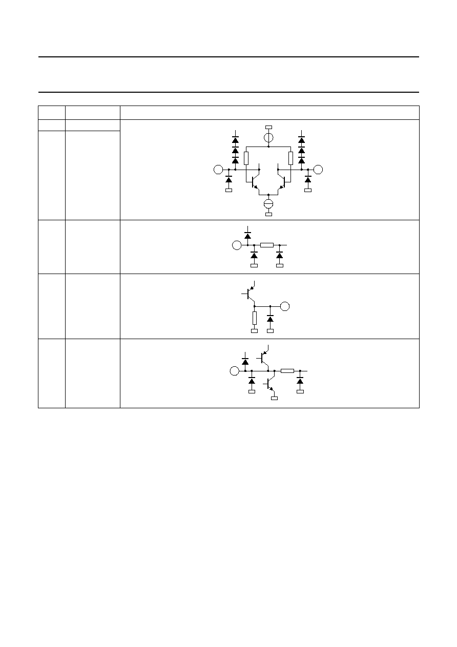
Internal pin configuration
PIN
SYMBOL
INTERNAL CIRCUIT
1
VCO_ON
4
S_DATA
6
S_EN
8
S_CLK
11
SLCCTR
7
RDATAP
9
DATAM
12
RSSI
14
RFB
15
RFA
17
R_ON
MGW234
1, 4, 6, 8, 11
MGW235
7, 9
MGW237
12
MGW238
14
15
17
MGW239
2001 Sep 06
20
Philips Semiconductors
Product specification
Fully integrated DECT transceiver
UAA3545
20
TXA
21
TXB
25
V
MOD
31
VREGO
32
CP/VCO
tune
PIN
SYMBOL
INTERNAL CIRCUIT
MGW240
20
21
25
MGW241
MGW242
31
32
MGW243
2001 Sep 06
21
Philips Semiconductors
Product specification
Fully integrated DECT transceiver
UAA3545
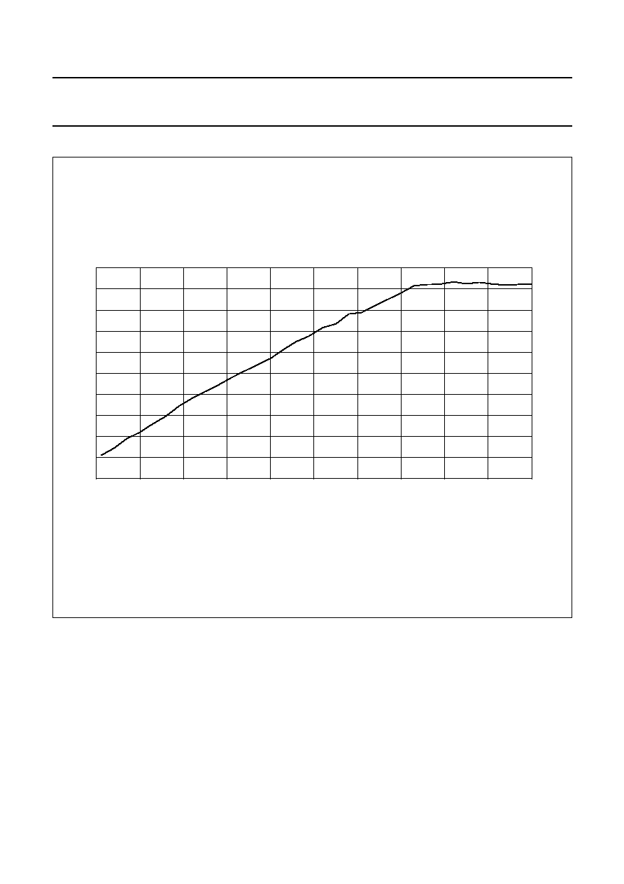
RECEIVED SIGNAL STRENGTH INTENSITY
handbook, full pagewidth
MGW233
0
2
1.6
0
-
100
-
70
-
60
-
50
-
40
-
80
-
90
-
30
-
20
Pi(RFA/B) (dBm)
-
10
0.4
0.8
1.2
VRSSI
(V)
Fig.7 RSSI output as a function of input power at pins RFA and RFB.

2001 Sep 06
22
Philips Semiconductors
Product specification
Fully integrated DECT transceiver
UAA3545
PACKAGE OUTLINE
0.2
UNIT
A
max.
A
1
A
2
A
3
b
p
c
E
(1)
e
H
E
L
L
p
Z
y
w
v
REFERENCES
OUTLINE
VERSION
EUROPEAN
PROJECTION
ISSUE DATE
IEC
JEDEC
EIAJ
mm
1.60
0.15
0.05
1.5
1.3
0.25
0.27
0.17
0.18
0.12
5.1
4.9
0.5
7.15
6.85
1.0
0.95
0.55
7
0
o
o
0.12
0.1
DIMENSIONS (mm are the original dimensions)
Note
1. Plastic or metal protrusions of 0.25 mm maximum per side are not included.
0.75
0.45
SOT401-1
136E01
MS-026
99-12-27
00-01-19
D
(1)
(1)
(1)
5.1
4.9
H
D
7.15
6.85
E
Z
0.95
0.55
D
b
p
e
E
B
8
D
H
b
p
E
H
v
M
B
D
ZD
A
Z E
e
v
M
A
X
1
32
25
24
17
16
9
A
1
A
L
p
detail X
L
(A )
3
A
2
y
w
M
w
M
0
2.5
5 mm
scale
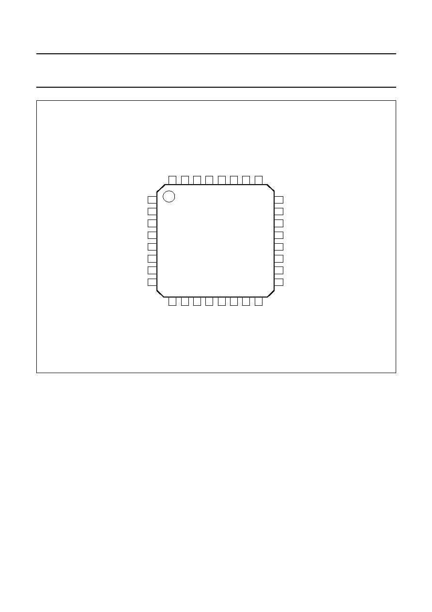
LQFP32: plastic low profile quad flat package; 32 leads; body 5 x 5 x 1.4 mm
SOT401-1
c
pin 1 index

2001 Sep 06
23
Philips Semiconductors
Product specification
Fully integrated DECT transceiver
UAA3545
SOLDERING
Introduction to soldering surface mount packages
This text gives a very brief insight to a complex technology.
A more in-depth account of soldering ICs can be found in
our
"Data Handbook IC26; Integrated Circuit Packages"
(document order number 9398 652 90011).
There is no soldering method that is ideal for all surface
mount IC packages. Wave soldering can still be used for
certain surface mount ICs, but it is not suitable for fine pitch
SMDs. In these situations reflow soldering is
recommended.
Reflow soldering
Reflow soldering requires solder paste (a suspension of
fine solder particles, flux and binding agent) to be applied
to the printed-circuit board by screen printing, stencilling or
pressure-syringe dispensing before package placement.
Several methods exist for reflowing; for example,
convection or convection/infrared heating in a conveyor
type oven. Throughput times (preheating, soldering and
cooling) vary between 100 and 200 seconds depending
on heating method.
Typical reflow peak temperatures range from
215 to 250
∞
C. The top-surface temperature of the
packages should preferable be kept below 220
∞
C for
thick/large packages, and below 235
∞
C for small/thin
packages.
Wave soldering
Conventional single wave soldering is not recommended
for surface mount devices (SMDs) or printed-circuit boards
with a high component density, as solder bridging and
non-wetting can present major problems.
To overcome these problems the double-wave soldering
method was specifically developed.
If wave soldering is used the following conditions must be
observed for optimal results:
∑
Use a double-wave soldering method comprising a
turbulent wave with high upward pressure followed by a
smooth laminar wave.
∑
For packages with leads on two sides and a pitch (e):
≠ larger than or equal to 1.27 mm, the footprint
longitudinal axis is preferred to be parallel to the
transport direction of the printed-circuit board;
≠ smaller than 1.27 mm, the footprint longitudinal axis
must be parallel to the transport direction of the
printed-circuit board.
The footprint must incorporate solder thieves at the
downstream end.
∑
For packages with leads on four sides, the footprint must
be placed at a 45
∞
angle to the transport direction of the
printed-circuit board. The footprint must incorporate
solder thieves downstream and at the side corners.
During placement and before soldering, the package must
be fixed with a droplet of adhesive. The adhesive can be
applied by screen printing, pin transfer or syringe
dispensing. The package can be soldered after the
adhesive is cured.
Typical dwell time is 4 seconds at 250
∞
C.
A mildly-activated flux will eliminate the need for removal
of corrosive residues in most applications.
Manual soldering
Fix the component by first soldering two
diagonally-opposite end leads. Use a low voltage (24 V or
less) soldering iron applied to the flat part of the lead.
Contact time must be limited to 10 seconds at up to
300
∞
C.
When using a dedicated tool, all other leads can be
soldered in one operation within 2 to 5 seconds between
270 and 320
∞
C.

2001 Sep 06
24
Philips Semiconductors
Product specification
Fully integrated DECT transceiver
UAA3545
Suitability of surface mount IC packages for wave and reflow soldering methods
Notes
1. All surface mount (SMD) packages are moisture sensitive. Depending upon the moisture content, the maximum
temperature (with respect to time) and body size of the package, there is a risk that internal or external package
cracks may occur due to vaporization of the moisture in them (the so called popcorn effect). For details, refer to the
Drypack information in the
"Data Handbook IC26; Integrated Circuit Packages; Section: Packing Methods".
2. These packages are not suitable for wave soldering as a solder joint between the printed-circuit board and heatsink
(at bottom version) can not be achieved, and as solder may stick to the heatsink (on top version).
3. If wave soldering is considered, then the package must be placed at a 45
∞
angle to the solder wave direction.
The package footprint must incorporate solder thieves downstream and at the side corners.
4. Wave soldering is only suitable for LQFP, TQFP and QFP packages with a pitch (e) equal to or larger than 0.8 mm;
it is definitely not suitable for packages with a pitch (e) equal to or smaller than 0.65 mm.
5. Wave soldering is only suitable for SSOP and TSSOP packages with a pitch (e) equal to or larger than 0.65 mm; it is
definitely not suitable for packages with a pitch (e) equal to or smaller than 0.5 mm.
PACKAGE
SOLDERING METHOD
WAVE
REFLOW
(1)
BGA, HBGA, LFBGA, SQFP, TFBGA
not suitable
suitable
HBCC, HLQFP, HSQFP, HSOP, HTQFP, HTSSOP, HVQFN, SMS
not suitable
(2)
suitable
PLCC
(3)
, SO, SOJ
suitable
suitable
LQFP, QFP, TQFP
not recommended
(3)(4)
suitable
SSOP, TSSOP, VSO
not recommended
(5)
suitable

2001 Sep 06
25
Philips Semiconductors
Product specification
Fully integrated DECT transceiver
UAA3545
DATA SHEET STATUS
Notes
1. Please consult the most recently issued data sheet before initiating or completing a design.
2. The product status of the device(s) described in this data sheet may have changed since this data sheet was
published. The latest information is available on the Internet at URL http://www.semiconductors.philips.com.
DATA SHEET STATUS
(1)
PRODUCT
STATUS
(2)
DEFINITIONS
Objective specification
Development
This data sheet contains data from the objective specification for product
development. Philips Semiconductors reserves the right to change the
specification in any manner without notice.
Preliminary specification
Qualification
This data sheet contains data from the preliminary specification.
Supplementary data will be published at a later date. Philips
Semiconductors reserves the right to change the specification without
notice, in order to improve the design and supply the best possible
product.
Product specification
Production
This data sheet contains data from the product specification. Philips
Semiconductors reserves the right to make changes at any time in order
to improve the design, manufacturing and supply. Changes will be
communicated according to the Customer Product/Process Change
Notification (CPCN) procedure SNW-SQ-650A.
DEFINITIONS
Short-form specification
The data in a short-form
specification is extracted from a full data sheet with the
same type number and title. For detailed information see
the relevant data sheet or data handbook.
Limiting values definition
Limiting values given are in
accordance with the Absolute Maximum Rating System
(IEC 60134). Stress above one or more of the limiting
values may cause permanent damage to the device.
These are stress ratings only and operation of the device
at these or at any other conditions above those given in the
Characteristics sections of the specification is not implied.
Exposure to limiting values for extended periods may
affect device reliability.
Application information
Applications that are
described herein for any of these products are for
illustrative purposes only. Philips Semiconductors make
no representation or warranty that such applications will be
suitable for the specified use without further testing or
modification.
DISCLAIMERS
Life support applications
These products are not
designed for use in life support appliances, devices, or
systems where malfunction of these products can
reasonably be expected to result in personal injury. Philips
Semiconductors customers using or selling these products
for use in such applications do so at their own risk and
agree to fully indemnify Philips Semiconductors for any
damages resulting from such application.
Right to make changes
Philips Semiconductors
reserves the right to make changes, without notice, in the
products, including circuits, standard cells, and/or
software, described or contained herein in order to
improve design and/or performance. Philips
Semiconductors assumes no responsibility or liability for
the use of any of these products, conveys no licence or title
under any patent, copyright, or mask work right to these
products, and makes no representations or warranties that
these products are free from patent, copyright, or mask
work right infringement, unless otherwise specified.

2001 Sep 06
26
Philips Semiconductors
Product specification
Fully integrated DECT transceiver
UAA3545
NOTES

2001 Sep 06
27
Philips Semiconductors
Product specification
Fully integrated DECT transceiver
UAA3545
NOTES

© Koninklijke Philips Electronics N.V. 2001
SCA73
All rights are reserved. Reproduction in whole or in part is prohibited without the prior written consent of the copyright owner.
The information presented in this document does not form part of any quotation or contract, is believed to be accurate and reliable and may be changed
without notice. No liability will be accepted by the publisher for any consequence of its use. Publication thereof does not convey nor imply any license
under patent- or other industrial or intellectual property rights.
Philips Semiconductors ≠ a worldwide company
Contact information
For additional information please visit http://www.semiconductors.philips.com.
Fax: +31 40 27 24825
For sales offices addresses send e-mail to: sales.addresses@www.semiconductors.philips.com.
Printed in The Netherlands
403506/01/pp
28
Date of release:
2001 Sep 06
Document order number:
9397 750 08151