 | –≠–ª–µ–∫—Ç—Ä–æ–Ω–Ω—ã–π –∫–æ–º–ø–æ–Ω–µ–Ω—Ç: UBA2014 | –°–∫–∞—á–∞—Ç—å:  PDF PDF  ZIP ZIP |
Document Outline
- FEATURES
- GENERAL DESCRIPTION
- APPLICATIONS
- ORDERING INFORMATION
- QUICK REFERENCE DATA
- BLOCK DIAGRAM
- PINNING
- FUNCTIONAL DESCRIPTION
- LIMITING VALUES
- THERMAL CHARACTERISTICS
- QUALITY SPECIFICATION
- CHARACTERISTICS
- APPLICATION INFORMATION
- PACKAGE OUTLINES
- SOLDERING
- DATA SHEET STATUS
- DEFINITIONS
- DISCLAIMERS
DATA SHEET
Product specification
2002 May 16
INTEGRATED CIRCUITS
UBA2014
600 V driver IC for HF fluorescent
lamps
2002 May 16
2
Philips Semiconductors
Product specification
600 V driver IC for HF fluorescent lamps
UBA2014
FEATURES
∑
Adjustable preheat time
∑
Adjustable preheat current
∑
Current controlled operating
∑
Single ignition attempt
∑
Adaptive non-overlap time control
∑
Integrated high-voltage level-shift function
∑
Power-down function
∑
Protection against lamp failures or lamp removal
∑
Capacitive mode protection.
APPLICATIONS
The circuit topology enables a broad range of ballast
applications at different mains voltages for driving lamp
types from e.g. T8, T5, PLC, T10, T12, PLL and PLT.
GENERAL DESCRIPTION
The IC is a monolithic integrated circuit for driving
electronically ballasted fluorescent lamps, with mains
voltages up to 277 V (RMS) (nominal value).
The circuit is made in a 650 V BCD power-logic process.
It provides the drive function for the 2 discrete power
MOSFETs.
Beside the drive function the IC also includes the level-shift
circuit, the oscillator function, a lamp voltage monitor, a
current control function, a timer function and protections.
ORDERING INFORMATION
TYPE
NUMBER
PACKAGE
NAME
DESCRIPTION
VERSION
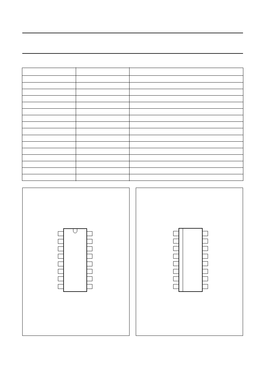
UBA2014T
SO16
plastic small outline package; 16 leads; body width 3.9 mm
SOT109-1
UBA2014P
DIP16
plastic dual in-line package; 16 leads (300 mil); long body
SOT38-1
2002 May 16
3
Philips Semiconductors
Product specification
600 V driver IC for HF fluorescent lamps
UBA2014
QUICK REFERENCE DATA
All voltages are referenced to GND; V
DD
= 13 V; V
FVDD
-
V
SH
= 13 V; T
amb
= 25
∞
C; unless otherwise specified; see
Chapter "Application information".
SYMBOL
PARAMETER
CONDITIONS
MIN.
TYP.
MAX.
UNIT
High-voltage supply
V
HS
high side supply voltage
I
HS
< 30
µ
A; t < 1 s
-
-
600
V
Start-up state
V
DD(start)
oscillator start voltage
12.4
13.0
13.6
V
V
DD(stop)
oscillator stop voltage
-
9.1
-
V
I
DD(start)
start-up current
V
DD
< V
DD(start)
-
170
200
µ
A
Reference voltage
V
Vref
reference voltage
I
L
= 10
µ
A
-
2.95
-
V
Voltage controlled oscillator
f
max
maximum bridge
frequency
-
100
-
kHz
f
min
minimum bridge frequency
38.9
40.5
42.1
kHz
Output drivers
I
source(GH)
output driver source
current
V
GH
-
V
SH
= 0; V
GL
= 0
-
180
-
mA
I
sink(GH)
output driver sink current
V
GH
-
V
SH
= 13 V
-
300
-
mA
Preheat current sensor
V
ph
preheat voltage level
-
0.60
-
V
Lamp voltage sensor
V
lamp(fail)
lamp fail voltage level at
pin LVS
0.77
0.81
0.85
V
V
lamp(max)
maximum lamp voltage
level at pin LVS
1.44
1.49
1.54
V
Average current sensor
V
offset
offset voltage
V
CS
= 0 to 2.5 V
-
2
0
+2
mV
g
m
transconductance
f = 1 kHz
-
3800
-
µ
A/mV
Timer
t
ph
preheat time
C
CT
= 330 nF;
R
IREF
= 33 k
1.6
1.8
2.0
s
V
OL(CT)
LOW-level output voltage
at pin CT
-
1.4
-
V
V
OH(CT)
HIGH-level output voltage
at pin CT
-
3.6
-
V
2002
May
16
4
Philips Semiconductors
Product specification
600 V dr
iv
er IC f
or HF fluorescent lamps
UBA2014
This text is here in white to force landscape pages to be rotated correctly when browsing through the pdf in the Acrobat reader.This text is here in
_
white to force landscape pages to be rotated correctly when browsing through the pdf in the Acrobat reader.This text is here inThis text is here in
white to force landscape pages to be rotated correctly when browsing through the pdf in the Acrobat reader. white to force landscape pages to be ...
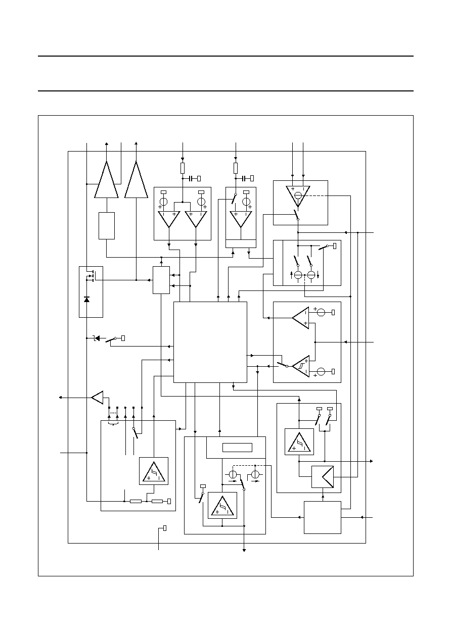
BLOCK DIA
GRAM
n
dbook, full pagewidth
MGW579
DRIVER
LOGIC
LEVEL
SHIFTER
BOOTSTRAP
FREQUENCY
CONTROL
AVERAGE
CURRENT
SENSOR
CS
+
15
GH
10
FVDD
9
CS
-
16
LOGIC
LAMP
VOLTAGE
SENSOR
VOLTAGE
CONTROLLED
OSCILLATOR
REFERENCE
CURRENT
I
V
GL
LS
DRIVER
HS
DRIVER
6
SH
11
ACM
12
PREHEAT TIMER
STATE LOGIC
∑
reset state
∑
start-up state
∑
preheat state
∑
ignition state
∑
burn state
∑
hold state
∑
power-down state
SUPPLY
VDD
Vref
reset
VDD(L)
Vpd
reference
voltages
digital
analog
supply (5 V)
3 V
7
14
LOGIC
COUNTER
1
4
CT
IREF
3
CF
13
LVS
2
CSW
5
GND
Vlamp(fail) Vlamp(max)
ANT/CMD
UBA2014
PCS
8
PCS
LOGIC
Fig.1 Block diagram.
2002 May 16
5
Philips Semiconductors
Product specification
600 V driver IC for HF fluorescent lamps
UBA2014
PINNING
SYMBOL
PIN
DESCRIPTION
CT
1
preheat timer output
CSW
2
voltage controlled oscillator input
CF
3
oscillator output
IREF
4
internal reference current input
GND
5
ground
GL
6
gate output for the low-side switch
V
DD
7
low-voltage supply
PCS
8
preheat current sensor input
F
VDD
9
floating supply, supply for the high-side switch
GH
10
gate output for the high-side switch
SH
11
source of the high-side switch
ACM
12
capacitive mode input
LVS
13
lamp voltage sensor input
V
ref
14
reference voltage output
CS+
15
positive input for the average current sensor
CS
-
16
negative input for the average current sensor
handbook, halfpage
UBA2014P
MGW580
1
2
3
4
5
6
7
8
16
15
14
13
12
11
10
9
CT
CSW
CF
IREF
GND
GL
VDD
PCS
FVDD
GH
SH
ACM
LVS
Vref
CS
+
CS
-
Fig.2 Pin configuration (DIP16).
handbook, halfpage
UBA2014T
MGW581
1
2
3
4
5
6
7
8
16
15
14
13
12
11
10
9
CT
CSW
CF
IREF
GND
GL
VDD
PCS
FVDD
GH
SH
ACM
LVS
Vref
CS
+
CS
-
Fig.3 Pin configuration (SO16).

2002 May 16
6
Philips Semiconductors
Product specification
600 V driver IC for HF fluorescent lamps
UBA2014
FUNCTIONAL DESCRIPTION
Start-up state
Initial start-up can be achieved by charging the low voltage
supply capacitor C7 (see Fig.8) via an external start-up
resistor. Start-up of the circuit is achieved under the
condition that both half-bridge transistors TR1 and TR2
are non-conductive. The circuit will be reset in the start-up
state. If the low voltage supply (V
DD
) reaches the value of
V
DD(H)
the circuit will start oscillating. A DC reset circuit is
incorporated in the High-Side (HS) driver. Below the
lock-out voltage at the F
VDD
pin the output voltage
(V
GH
-
V
SH
) is zero. The voltages at pins CF and CT are
zero during the start-up state.
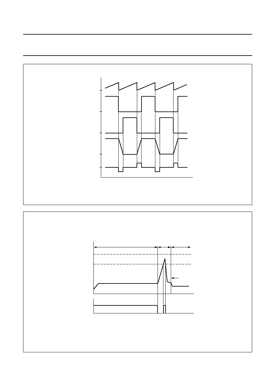
Oscillation
The internal oscillator is a Voltage-Controlled Oscillator
circuit (VCO) which generates a sawtooth waveform
between the CF
high
level and 0 V. The frequency of the
sawtooth is determined by capacitor C
CF
, resistor R
IREF
,
and the voltage at pin CSW. The minimum and maximum
switching frequencies are determined by R
IREF
and C
CF
;
their ratio is internally fixed. The sawtooth frequency is
twice the half-bridge frequency. The UBA2014 brings the
transistors TR1 and TR2 into conduction alternately with a
duty cycle of approximately 50%. An overview of the
oscillator signal and driver signals is illustrated in Fig.4.
The oscillator starts oscillating at f
max
. During the first
switching cycle the Low-Side (LS) transistor is switched
on. The first conducting time is made extra long to enable
the bootstrap capacitor to charge.
Adaptive non-overlap
The non-overlap time is realized with an adaptive
non-overlap circuit (ANT). By using an adaptive
non-overlap circuit, the application can determine the
duration of the non-overlap time and make it optimum for
each frequency (see Fig.4). The non-overlap time is
determined by the slope of the half-bridge voltage, and is
detected by the signal across resistor R16 which is
connected directly to pin ACM. The minimum non-overlap
time is internally fixed. The maximum non-overlap time is
internally fixed at approximately 25% of the bridge period
time. An internal filter of 30 ns is included at the ACM pin
to increase the noise immunity.
Timing circuit
A timing circuit is included to determine the preheat time
and the ignition time. The circuit consists of a clock
generator and a counter.
The preheat time is defined by C
CT
and R
IREF
and consists
of 7 pulses at C
CT
; the maximum ignition time is 1 pulse at
C
CT
. The timing circuit starts operating after the start-up
state, as soon as the low supply voltage (V
DD
) has reached
V
DD(H)
or when a critical value of the lamp voltage
(V
lamp(fail)
) is exceeded. When the timer is not operating
C
CT
is discharged to 0 V at 1 mA.
Preheat state
After starting at f
max
, the frequency decreases until the
momentary value of the voltage across sense resistor R14
reaches the internally fixed preheat voltage level (pin
PCS). At crossing the preheat voltage level, the output
current of the Preheat Current Sensor circuit (PCS)
discharges the capacitor C
CSW
, thus raising the frequency.
The preheat time begins at the moment that the circuit
starts oscillating. During the preheat time the Average
Current Sensor circuit (ACS) is disabled. An internal filter
of 30 ns is included at pin PCS to increase the noise
immunity.
Ignition state
After the preheat time the ignition state is entered and the
frequency will sweep down due to charging of the
capacitor at pin CSW with an internally fixed current; see
Fig.5. During this continuous decrease in frequency, the
circuit approaches the resonant frequency of the load. This
will cause a high voltage across the load, which normally
ignites the lamp. The ignition voltage of a lamp is designed
above the V
lamp(fail)
level. If the lamp voltage exceeds the
V
lamp(fail)
level the ignition timer is started.
Burn state
If the lamp voltage does not exceed the V
lamp(max)
level the
voltage at pin CSW will continue to increase until the clamp
level at pin CSW is reached; see Fig.5. As a consequence
the frequency will decrease until the minimum frequency is
reached.
When the frequency reaches its minimum level it is
assumed that the lamp has ignited and the circuit enters
the burn state. The Average Current Sensor circuit (ACS)
will be enabled. As soon as the averaged voltage across
sense resistor R14, measured at pin CS
-
, reaches the
reference level at pin CS+, the average current sensor
circuit will take over the control of the lamp current. The
average current through R14 is transferred to a voltage at
the voltage controlled oscillator and regulates the
frequency and, as a result, the lamp current.

2002 May 16
7
Philips Semiconductors
Product specification
600 V driver IC for HF fluorescent lamps
UBA2014
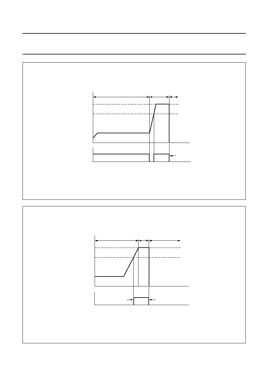
Lamp failure mode
D
URING IGNITION STATE
If the lamp does not ignite, the voltage level increases.
When the lamp voltage exceeds the V
lamp(max)
level, the
voltage will be regulated at the V
lamp(max)
level; see Fig.6.
At crossing the V
lamp(fail)
level the ignition timer was
already started. If the voltage at pin LVS is above the
V
lamp(fail)
level at the end of the ignition time the circuit
stops oscillating and is forced in a Power-down mode. The
circuit will be reset only when the supply voltage is
powered-down.
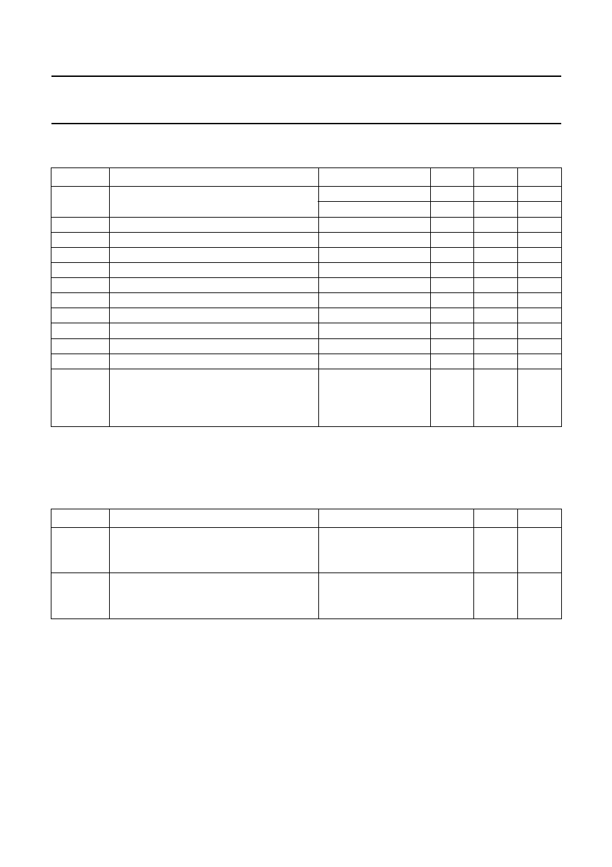
D
URING BURN STATE
If the lamp fails during normal operation, the voltage
across the lamp will increase and the lamp voltage will
exceed the V
lamp(fail)
level; see Fig.7. At that moment the
ignition timer is started. If the lamp voltage increases
further it will reach the V
lamp(max)
level. This forces the
circuit to re-enter the ignition state and results in an
attempt to re-ignite the lamp. If during restart the lamp still
fails, the voltage remains high until the end of the ignition
time. At the end of the ignition time the circuit stops
oscillating and the circuit will enter in the Power-down
mode.
Power-down state
The Power-down state will be entered if, at the end of the
ignition time, the voltage at pin LVS is above V
lamp(fail)
.
In the Power-down mode the oscillator will be stopped and
both TR1 and TR2 will be non-conductive. The V
DD
supply
is internally clamped. The circuit is released from the
Power-down state by lowering the low voltage supply
below V
DD(reset)
.
Capacitive mode protection
The signal across R16 also gives information about the
switching behaviour of the half bridge.
If, after the preheat state, the voltage across the ACM
resistor (R16) does not exceed the V
CMD
level during the
non-overlap time, the Capacitive Mode Detection circuit
(CMD) assumes that the circuit is in the capacitive mode
of operation. As a consequence the frequency will directly
be increased to f
max
. The frequency behaviour is
decoupled from the voltage at pin CSW until C
CSW
has
been discharged to zero.
Charge coupling
Due to parasitic capacitive coupling to the high voltage
circuitry all pins are burdened with a repetitive charge
injection. Given the typical application the pins IREF and
CF are sensitive to this charge injection. For charge
coupling of
±
8 pC, a safe functional operation of the IC is
guaranteed, independent of the current level.
Charge coupling at current levels below 50
µ
A will not
interfere with the accuracy of the V
CS
, V
PCS
and V
ACM
levels.
Charge coupling at current levels below 20
µ
A will not
interfere with the accuracy of any parameter.
Design equations
The following design equations are used to calculate the
desired preheat time, the maximum ignition time, and the
minimum and the maximum switching frequency.
t
ph
= 1.7
◊
10
-
4
◊
C
CT
◊
R
IREF
(s)
t
ign
= 3.1
◊
10
-
5
◊
C
CT
◊
R
IREF
(s)
in kHz
f
max
= 2.5
◊
f
min
(kHz)
with C
CT
in nF, R
IREF
in k
, and C
CF
in pF. Start of ignition
is defined as the moment at which the measured lamp
voltage crosses the V
lamp(fail)
level; see Section "Lamp
failure mode".
f
min
125
10
3
◊
C
CF
R
IREF
◊
(
)
-------------------------------------
=
2002 May 16
8
Philips Semiconductors
Product specification
600 V driver IC for HF fluorescent lamps
UBA2014
handbook, full pagewidth
MGW582
VCF
VGL
V(GH-SH)
0
0
0
time
0
0
VACM
Vhb
Fig.4 Oscillator and driver signals.
handbook, full pagewidth
MGW583
burn state
ignition
state
preheat state
fmin detection
Timer
on
time
off
Vlamp(fail)
Vlamp(max)
Vlamp
Fig.5 Normal ignition behaviour.
2002 May 16
9
Philips Semiconductors
Product specification
600 V driver IC for HF fluorescent lamps
UBA2014
handbook, full pagewidth
MGW584
power-down
state
preheat state
ignition
state
timer
ended
Timer
on
time
off
Vlamp(fail)
Vlamp(max)
Vlamp
Fig.6 Failure mode during ignition.
handbook, full pagewidth
MGW585
time
Timer
on
off
Vlamp(fail)
Vlamp(max)
Vlamp
power-down
state
burn state
ignition
state
timer
ended
timer
started
Fig.7 Failure mode during burn.
2002 May 16
10
Philips Semiconductors
Product specification
600 V driver IC for HF fluorescent lamps
UBA2014
LIMITING VALUES
In according with the Absolute Maximum Rating System (IEC 60134); voltages with respect to pin GND.
Note
1. In accordance with the human body model, i.e. equivalent to discharging a 100 pF capacitor through a 1.5 k
series
resistor.
THERMAL CHARACTERISTICS
QUALITY SPECIFICATION
In accordance with
`SNW-FQ-611-E'.
SYMBOL
PARAMETER
CONDITIONS
MIN.
MAX.
UNIT
V
HS
high side supply voltage
I
HS
< 30
µ
A; t < 1 s
600
-
V
I
HS
< 30
µ
A
510
-
V
V
DD(max)
maximum voltage at pin V
DD
-
14
V
V
ACM(max)
maximum voltage at pin ACM
-
5
+5
V
V
PCS(max)
maximum voltage at pin PCS
-
5
+5
V
V
LVS(max)
maximum voltage at pin LVS
0
5
V
V
CS+(max)
maximum voltage at pin CS+
0
5
V
V
CS
-
(max)
maximum voltage at pin CS
-
-
0.3
+5
V
V
CSW(max)
maximum voltage at pin CSW
0
5
V
T
amb
ambient temperature
-
25
+80
∞
C
T
j
junction temperature
-
25
+150
∞
C
T
stg
storage temperature
-
55
+150
∞
C
V
esd
electrostatic handling voltage
note 1
pins F
VDD
, GH, and SH
-
±
1000
V
pins CT, CSW, CF, IREF, GL, V
DD
, PCS,
CS
-
, CS+, V
ref
, LVS, and ACM
-
±
2500
V
SYMBOL
PARAMETER
CONDITIONS
VALUE
UNIT
R
th(j-a)
thermal resistance from junction to ambient
in free air
SO16
100
K/W
DIP16
60
K/W
R
th(j-pin)
thermal resistance from junction to PCB
in free air
SO16
50
K/W
DIP16
30
K/W
2002 May 16
11
Philips Semiconductors
Product specification
600 V driver IC for HF fluorescent lamps
UBA2014
CHARACTERISTICS
All voltages referenced to GND; V
DD
= 13 V; V
FVDD
-
V
SH
= 13 V; T
amb
= 25
∞
C; unless otherwise specified; see
Chapter "Application information".
SYMBOL
PARAMETER
CONDITIONS
MIN.
TYP.
MAX.
UNIT
High-voltage supply
I
leak
leakage current on high-voltage
pins
voltage at pins F
VDD
, GH
and SH = 600 V
-
-
30
µ
A
Start-up state
V
DD
supply voltage for defined driver
output
TR1 = off; TR2 = off
-
-
6
V
V
DD(start)
oscillator start voltage
12.4
13.0
13.6
V
V
DD(low)
oscillator stop voltage
8.6
9.1
9.6
V
V
DD(hys)
start-stop hysteresis
3.5
3.9
4.4
V
I
DD(start)
start-up current
V
DD
< V
DD(start)
-
170
200
µ
A
V
DD(clamp)
clamp voltage
Power-down mode
10
11
12
V
I
pd
power-down current
V
DD
= 9 V
-
170
200
µ
A
V
DD(reset)
reset voltage
TR1 = off; TR2 = off
4.5
5.5
7.0
V
I
DD
operating supply current
f
bridge
= 40 kHz without gate
drive
-
1.5
2.2
mA
Reference voltage
V
Vref
reference voltage
I
L
= 10
µ
A
2.86
2.95
3.04
V
I
source(Vref)
source current capability
1
-
-
mA
I
sink(Vref)
sink current capability
1
-
-
mA
Z
Vref
output impedance
I
L
= 1 mA source
-
3.0
-
V
Vref
/
T
temperature coefficient
I
L
= 10
µ
A;
T
amb
= 25 to 150
∞
C
-
-
0.64
-
%/K
Current supply
V
IREF
voltage at pin IREF
-
2.5
-
V
I
IREF
reference current range
65
-
95
µ
A
Voltage controlled oscillator
V
CSW
control voltage
2.7
3.0
3.3
V
V
clamp
clamp voltage
burn state
2.8
3.1
3.4
V
I
CF(start)
output oscillator start current
V
CF
= 1.5 V
3.8
4.5
5.2
µ
A
t
start
first output oscillator stroke time
-
50
-
µ
s
I
CF(min)
minimum output oscillator current
V
CF
= 1.5 V
-
21
-
µ
A
I
CF(max)
maximum output oscillator current
V
CF
= 1.5 V
-
54
-
µ
A
f
max
maximum bridge frequency
90
100
110
kHz
f
min
minimum bridge frequency
38.9
40.5
42.1
kHz
f
stab
frequency stability
T
amb
=
-
20 to +80
∞
C
-
1.3
-
%
V
CF(high)
high level output oscillator voltage
f = f
min
-
2.5
-
V
t
nc(min)
minimum non-overlap time
GH to GL
0.68
0.90
1.13
µ
s
GL to GH
0.75
1.00
1.25
µ
s
2002 May 16
12
Philips Semiconductors
Product specification
600 V driver IC for HF fluorescent lamps
UBA2014
t
no(max)
maximum non-overlap time
f
bridge
= 40 kHz; note 1
-
7.5
-
µ
s
Output drivers
I
o(source)(GH)
high side output source current
V
GH
-
V
SH
= 0
135
180
235
mA
I
o(sink)(GH)
high side output sink current
V
GH
-
V
SH
= 13 V
265
330
415
mA
I
o(source)(GL)
low side output source current
V
GL
= 0
135
200
235
mA
I
o(sink)(GL)
low side output sink current
V
GL
= 13 V
265
330
415
mA
V
OH(GH)(h)
HIGH-level high side output voltage I
o
= 10 mA
12.5
-
-
V
V
OL(GH)(h)
LOW-level high side output voltage
I
o
= 10 mA
-
-
0.5
V
V
OH(GL)(l)
HIGH-level low side output voltage
I
o
= 10 mA
12.5
-
-
V
V
OL(GL)(l)
LOW-level low side output voltage
I
o
= 10 mA
-
-
0.5
V
R
HS(on)
high side on resistance
I
o
= 10 mA
32
39
45
R
HS(off)
high side off resistance
I
o
= 10 mA
16
21
26
R
LS(on)
low side on resistance
I
o
= 10 mA
32
39
45
R
LS(off)
low side off resistance
I
o
= 10 mA
16
21
26
V
boot
bootstrap diode forward drop
voltage
I = 5 mA
1.3
1.7
2.1
V
V
FVDD
lockout voltage
2.8
3.5
4.2
V
I
FVDD
floating well supply current
DC level at
V
GH
-
V
SH
= 13 V
-
35
-
µ
A
Preheat current sensor
I
i(PCS)
input current
V
PCS
= 0.6 V
-
-
1
µ
A
V
ph
preheat voltage level at pin PCS
0.57
0.60
0.63
V
I
o(source)(CSW)
output source current
V
CSW
= 2.0 V
9.0
10
11
µ
A
I
o(sink)(CSW)
effective output sink current
V
CSW
= 2.0 V
-
10
-
µ
A
Adaptive non-overlap and capacitive mode detection
I
i(ACM)
input current
V
ACM
= 0.6 V
-
-
1
µ
A
V
CMD+
positive capacitive mode detection
voltage
80
100
120
mV
V
CMD
-
negative capacitive mode detection
voltage
-
68
-
85
-
102
mV
Lamp voltage sensor
I
i(LVS)
input current
V
LVS
= 0.81 V
-
-
1
µ
A
V
lamp(fail)
lamp fail voltage level at pin LVS
0.77
0.81
0.85
V
V
lamp(fail)(hys)
hysteresis lamp fail voltage level at
pin LVS
119
144
169
mV
V
lamp(max)
maximum lamp voltage level at pin
LVS
1.44
1.49
1.54
V
I
o(sink)(CSW)
output sink current
V
CSW
= 2.0 V
27
30
33
µ
A
I
o(source)(ign)
ignition output source current
V
CSW
= 2.0 V
9.0
10
11
µ
A
SYMBOL
PARAMETER
CONDITIONS
MIN.
TYP.
MAX.
UNIT
2002 May 16
13
Philips Semiconductors
Product specification
600 V driver IC for HF fluorescent lamps
UBA2014
Note
1. The maximum non-overlap is determined by the level of the CF signal. If this signal exceeds a level of 1.25 V the
non-overlap will end, resulting in a maximum non-overlap time of 7.5
µ
s at a bridge frequency of 40 kHz.
Average current sensor
I
i(CS)
input current
V
CS
= 0 V
-
-
1
µ
A
V
offset
offset voltage
V
CS+
= V
CS
-
= 0 to 2.5 V
-
2
0
+2
mV
g
m
transconductance
f = 1 kHz
1900
3800
5700
µ
A/mV
I
o(CSW)
output current
source and sink; V
CSW
= 2 V 85
95
105
µ
A
Timer
I
o(CT)
preheat timer output current
V
CT
= 2.5 V
5.5
5.9
6.3
µ
A
V
OL(CT)
LOW-level preheat timer output
voltage
-
1.4
-
V
V
OH(CT)
HIGH-level preheat timer output
voltage
-
3.6
-
V
V
hys(CT)
preheat timer output hysteresis
2.05
2.20
2.35
V
t
ph
preheat time
C
CT
= 330 nF and
R
IREF
= 33 k
1.6
1.8
2.0
s
t
ign
ignition time
C
CT
= 330 nF and
R
IREF
= 33 k
-
0.26
-
s
SYMBOL
PARAMETER
CONDITIONS
MIN.
TYP.
MAX.
UNIT
2002
May
16
14
Philips Semiconductors
Product specification
600 V dr
iv
er IC f
or HF fluorescent lamps
UBA2014
This text is here in white to force landscape pages to be rotated correctly when browsing through the pdf in the Acrobat reader.This text is here in
_
white to force landscape pages to be rotated correctly when browsing through the pdf in the Acrobat reader.This text is here inThis text is here in
white to force landscape pages to be rotated correctly when browsing through the pdf in the Acrobat reader. white to force landscape pages to be ...
APPLICA
TION INFORMA
TION
n
dbook, full pagewidth
MGW586
Vref
FVDD
Z1
12 V
GH
SH
GL
PCS
1
7
LVS
CS
-
CS
+
VDD
CT
9
10
11
6
4
5
3
2
14
8
ACM
12
13
16
15
CSW
CF
GND
IREF
C3
1 nF
C19
56 nF
C17
6.8 nF
C8
330 pF
C20
68 nF
TLD36W
C22
8.2 nF
C23
100 nF
C6
1.2 nF
C10
5.6 nF
C5
100 nF
VDC
400 V
UBA2014
HIGH SIDE
DRIVER
LOW SIDE
DRIVER
BOOTSTRAP
DRIVER
CONTROL
SUPPLY
PREHEAT
TIMER
REFERENCE
CURRENT
DIVIDER
ADAPTIVE
NON-OVERLAP TIMING
AND CAPACITIVE
MODE DETECTOR
PREHEAT
CURRENT
SENSOR
LAMP
VOLTAGE
SENSOR
-
+
+
AVERAGE
CURRENT
SENSOR
VOLTAGE
CONTROLLED
OSCILLATOR
R2
8.2
k
R12
33 k
R5
10 k
R18
180 k
R20
220 k
R4
1 M
D4
BYD77D
Lamp
R16
1.5
R1
1 M
R10
1 M
R3
220 k
R13
150
D1
BYD77D
R8
8.2 k
F1
1A
R9
47
L1
1.9 mH
TR1
IRF820
TR2
IRF820
C2
12 nF
C14
100 pF
C13
220 nF
C15
330 nF
C7
330 nF
R14
1
C24
100 nF
Fig.8 Test and application circuit.
2002 May 16
15
Philips Semiconductors
Product specification
600 V driver IC for HF fluorescent lamps
UBA2014
PACKAGE OUTLINES
X
w
M
A
A
1
A
2
b
p
D
H
E
L
p
Q
detail X
E
Z
e
c
L
v
M
A
(A )
3
A
8
9
1
16
y
pin 1 index
UNIT
A
max.
A
1
A
2
A
3
b
p
c
D
(1)
E
(1)
(1)
e
H
E
L
L
p
Q
Z
y
w
v
REFERENCES
OUTLINE
VERSION
EUROPEAN
PROJECTION
ISSUE DATE
IEC
JEDEC
EIAJ
mm
inches
1.75
0.25
0.10
1.45
1.25
0.25
0.49
0.36
0.25
0.19
10.0
9.8
4.0
3.8
1.27
6.2
5.8
0.7
0.6
0.7
0.3
8
0
o
o
0.25
0.1
DIMENSIONS (inch dimensions are derived from the original mm dimensions)
Note
1. Plastic or metal protrusions of 0.15 mm maximum per side are not included.
1.0
0.4
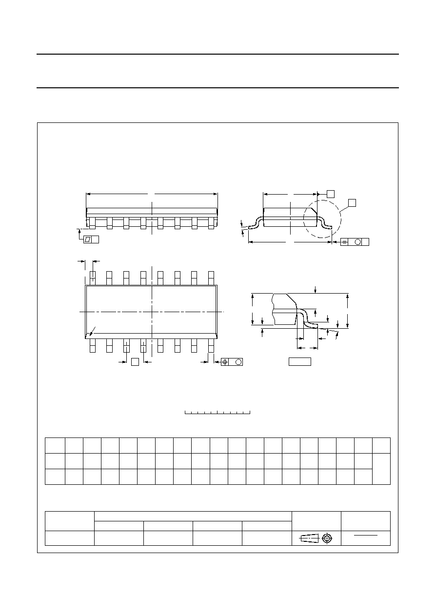
SOT109-1
97-05-22
99-12-27
076E07
MS-012
0.069
0.010
0.004
0.057
0.049
0.01
0.019
0.014
0.0100
0.0075
0.39
0.38
0.16
0.15
0.050
1.05
0.041
0.244
0.228
0.028
0.020
0.028
0.012
0.01
0.25
0.01
0.004
0.039
0.016
0
2.5
5 mm
scale
SO16: plastic small outline package; 16 leads; body width 3.9 mm
SOT109-1
2002 May 16
16
Philips Semiconductors
Product specification
600 V driver IC for HF fluorescent lamps
UBA2014
UNIT
A
max.
1
2
b
1
c
E
e
M
H
L
REFERENCES
OUTLINE
VERSION
EUROPEAN
PROJECTION
ISSUE DATE
IEC
JEDEC
EIAJ
mm
inches
DIMENSIONS (inch dimensions are derived from the original mm dimensions)
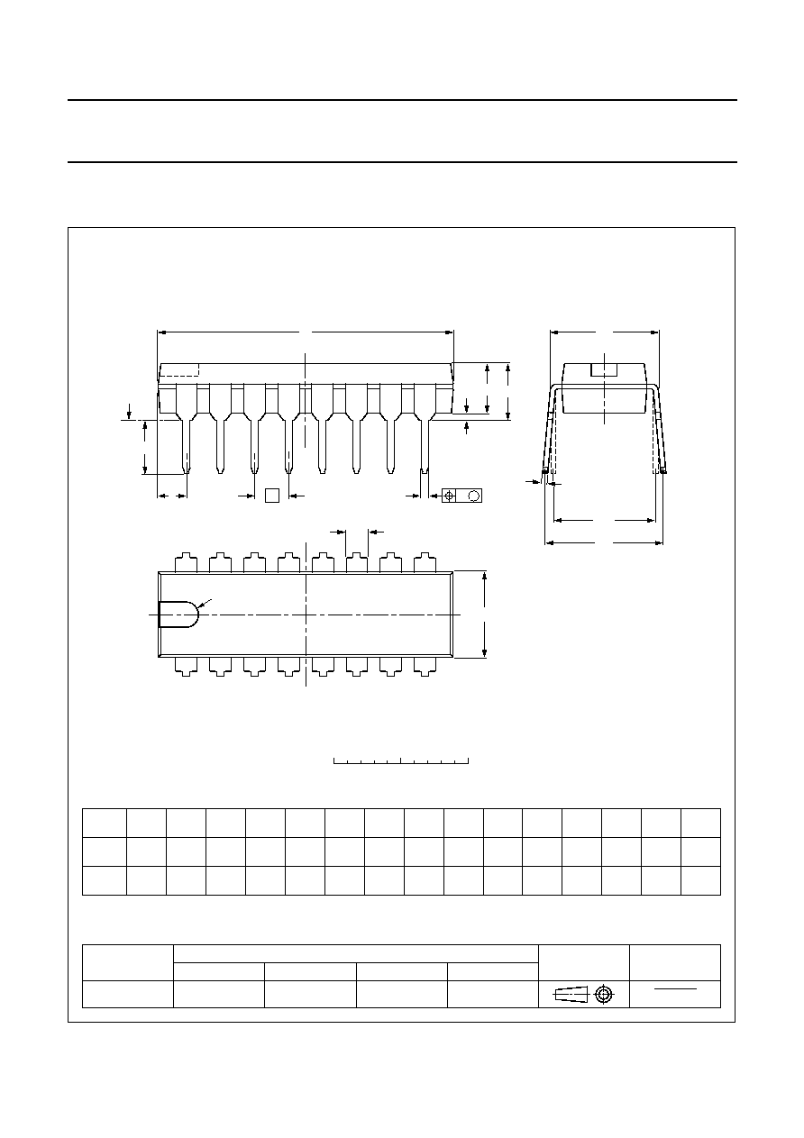
SOT38-1
95-01-19
99-12-27
A
min.
A
max.
b
max.
w
M
E
e
1
1.40
1.14
0.055
0.045
0.53
0.38
0.32
0.23
21.8
21.4
0.86
0.84
6.48
6.20
0.26
0.24
3.9
3.4
0.15
0.13
0.254
2.54
7.62
0.30
8.25
7.80
0.32
0.31
9.5
8.3
0.37
0.33
2.2
0.087
4.7
0.51
3.7
0.15
0.021
0.015
0.013
0.009
0.01
0.10
0.020
0.19
050G09
MO-001
SC-503-16
M
H
c
(e )
1
M
E
A
L
seating plane
A
1
w
M
b
1
e
D
A
2
Z
16
1
9
8
b
E
pin 1 index
0
5
10 mm
scale
Note
1. Plastic or metal protrusions of 0.25 mm maximum per side are not included.
(1)
(1)
D
(1)
Z
DIP16: plastic dual in-line package; 16 leads (300 mil); long body
SOT38-1

2002 May 16
17
Philips Semiconductors
Product specification
600 V driver IC for HF fluorescent lamps
UBA2014
SOLDERING
Introduction
This text gives a very brief insight to a complex technology.
A more in-depth account of soldering ICs can be found in
our
"Data Handbook IC26; Integrated Circuit Packages"
(document order number 9398 652 90011).
There is no soldering method that is ideal for all IC
packages. Wave soldering is often preferred when
through-hole and surface mount components are mixed on
one printed-circuit board. Wave soldering can still be used
for certain surface mount ICs, but it is not suitable for fine
pitch SMDs. In these situations reflow soldering is
recommended.
Through-hole mount packages
S
OLDERING BY DIPPING OR BY SOLDER WAVE
The maximum permissible temperature of the solder is
260
∞
C; solder at this temperature must not be in contact
with the joints for more than 5 seconds. The total contact
time of successive solder waves must not exceed
5 seconds.
The device may be mounted up to the seating plane, but
the temperature of the plastic body must not exceed the
specified maximum storage temperature (T
stg(max)
). If the
printed-circuit board has been pre-heated, forced cooling
may be necessary immediately after soldering to keep the
temperature within the permissible limit.
M
ANUAL SOLDERING
Apply the soldering iron (24 V or less) to the lead(s) of the
package, either below the seating plane or not more than
2 mm above it. If the temperature of the soldering iron bit
is less than 300
∞
C it may remain in contact for up to
10 seconds. If the bit temperature is between
300 and 400
∞
C, contact may be up to 5 seconds.
Surface mount packages
R
EFLOW SOLDERING
Reflow soldering requires solder paste (a suspension of
fine solder particles, flux and binding agent) to be applied
to the printed-circuit board by screen printing, stencilling or
pressure-syringe dispensing before package placement.
Several methods exist for reflowing; for example,
convection or convection/infrared heating in a conveyor
type oven. Throughput times (pre-heating, soldering and
cooling) vary between 100 and 200 seconds depending
on heating method.
Typical reflow peak temperatures range from
215 to 250
∞
C. The top-surface temperature of the
packages should preferable be kept below 220
∞
C for
thick/large packages, and below 235
∞
C for small/thin
packages.
W
AVE SOLDERING
Conventional single wave soldering is not recommended
for surface mount devices (SMDs) or printed-circuit boards
with a high component density, as solder bridging and
non-wetting can present major problems.
To overcome these problems the double-wave soldering
method was specifically developed.
If wave soldering is used the following conditions must be
observed for optimal results:
∑
Use a double-wave soldering method comprising a
turbulent wave with high upward pressure followed by a
smooth laminar wave.
∑
For packages with leads on two sides and a pitch (e):
≠ larger than or equal to 1.27 mm, the footprint
longitudinal axis is preferred to be parallel to the
transport direction of the printed-circuit board;
≠ smaller than 1.27 mm, the footprint longitudinal axis
must be parallel to the transport direction of the
printed-circuit board.
The footprint must incorporate solder thieves at the
downstream end.
∑
For packages with leads on four sides, the footprint must
be placed at a 45
∞
angle to the transport direction of the
printed-circuit board. The footprint must incorporate
solder thieves downstream and at the side corners.
During placement and before soldering, the package must
be fixed with a droplet of adhesive. The adhesive can be
applied by screen printing, pin transfer or syringe
dispensing. The package can be soldered after the
adhesive is cured.
Typical dwell time is 4 seconds at 250
∞
C.
A mildly-activated flux will eliminate the need for removal
of corrosive residues in most applications.
M
ANUAL SOLDERING
Fix the component by first soldering two
diagonally-opposite end leads. Use a low voltage (24 V or
less) soldering iron applied to the flat part of the lead.
Contact time must be limited to 10 seconds at up to
300
∞
C. When using a dedicated tool, all other leads can
be soldered in one operation within 2 to 5 seconds
between 270 and 320
∞
C.

2002 May 16
18
Philips Semiconductors
Product specification
600 V driver IC for HF fluorescent lamps
UBA2014
Suitability of IC packages for wave, reflow and dipping soldering methods
Notes
1. All surface mount (SMD) packages are moisture sensitive. Depending upon the moisture content, the maximum
temperature (with respect to time) and body size of the package, there is a risk that internal or external package
cracks may occur due to vaporization of the moisture in them (the so called popcorn effect). For details, refer to the
Drypack information in the
"Data Handbook IC26; Integrated Circuit Packages; Section: Packing Methods".
2. For SDIP packages, the longitudinal axis must be parallel to the transport direction of the printed-circuit board.
3. These packages are not suitable for wave soldering. On versions with the heatsink on the bottom side, the solder
cannot penetrate between the printed-circuit board and the heatsink. On versions with the heatsink on the top side,
the solder might be deposited on the heatsink surface.
4. If wave soldering is considered, then the package must be placed at a 45
∞
angle to the solder wave direction.
The package footprint must incorporate solder thieves downstream and at the side corners.
5. Wave soldering is only suitable for LQFP, QFP and TQFP packages with a pitch (e) equal to or larger than 0.8 mm;
it is definitely not suitable for packages with a pitch (e) equal to or smaller than 0.65 mm.
6. Wave soldering is only suitable for SSOP and TSSOP packages with a pitch (e) equal to or larger than 0.65 mm; it is
definitely not suitable for packages with a pitch (e) equal to or smaller than 0.5 mm.
MOUNTING
PACKAGE
SOLDERING METHOD
WAVE
REFLOW
(1)
DIPPING
Through-hole mount DBS, DIP, HDIP, SDIP, SIL
suitable
(2)
-
suitable
Surface mount
BGA, HBGA, LFBGA, SQFP, TFBGA
not suitable
suitable
-
HBCC, HLQFP, HSQFP, HSOP, HTQFP,
HTSSOP, HVQFN, SMS
not suitable
(3)
suitable
-
PLCC
(4)
, SO, SOJ
suitable
suitable
-
LQFP, QFP, TQFP
not recommended
(4)(5)
suitable
-
SSOP, TSSOP, VSO
not recommended
(6)
suitable
-

2002 May 16
19
Philips Semiconductors
Product specification
600 V driver IC for HF fluorescent lamps
UBA2014
DATA SHEET STATUS
Notes
1. Please consult the most recently issued data sheet before initiating or completing a design.
2. The product status of the device(s) described in this data sheet may have changed since this data sheet was
published. The latest information is available on the Internet at URL http://www.semiconductors.philips.com.
DATA SHEET STATUS
(1)
PRODUCT
STATUS
(2)
DEFINITIONS
Objective data
Development
This data sheet contains data from the objective specification for product
development. Philips Semiconductors reserves the right to change the
specification in any manner without notice.
Preliminary data
Qualification
This data sheet contains data from the preliminary specification.
Supplementary data will be published at a later date. Philips
Semiconductors reserves the right to change the specification without
notice, in order to improve the design and supply the best possible
product.
Product data
Production
This data sheet contains data from the product specification. Philips
Semiconductors reserves the right to make changes at any time in order
to improve the design, manufacturing and supply. Changes will be
communicated according to the Customer Product/Process Change
Notification (CPCN) procedure SNW-SQ-650A.
DEFINITIONS
Short-form specification
The data in a short-form
specification is extracted from a full data sheet with the
same type number and title. For detailed information see
the relevant data sheet or data handbook.
Limiting values definition
Limiting values given are in
accordance with the Absolute Maximum Rating System
(IEC 60134). Stress above one or more of the limiting
values may cause permanent damage to the device.
These are stress ratings only and operation of the device
at these or at any other conditions above those given in the
Characteristics sections of the specification is not implied.
Exposure to limiting values for extended periods may
affect device reliability.
Application information
Applications that are
described herein for any of these products are for
illustrative purposes only. Philips Semiconductors make
no representation or warranty that such applications will be
suitable for the specified use without further testing or
modification.
DISCLAIMERS
Life support applications
These products are not
designed for use in life support appliances, devices, or
systems where malfunction of these products can
reasonably be expected to result in personal injury. Philips
Semiconductors customers using or selling these products
for use in such applications do so at their own risk and
agree to fully indemnify Philips Semiconductors for any
damages resulting from such application.
Right to make changes
Philips Semiconductors
reserves the right to make changes, without notice, in the
products, including circuits, standard cells, and/or
software, described or contained herein in order to
improve design and/or performance. Philips
Semiconductors assumes no responsibility or liability for
the use of any of these products, conveys no licence or title
under any patent, copyright, or mask work right to these
products, and makes no representations or warranties that
these products are free from patent, copyright, or mask
work right infringement, unless otherwise specified.

© Koninklijke Philips Electronics N.V. 2002
SCA74
All rights are reserved. Reproduction in whole or in part is prohibited without the prior written consent of the copyright owner.
The information presented in this document does not form part of any quotation or contract, is believed to be accurate and reliable and may be changed
without notice. No liability will be accepted by the publisher for any consequence of its use. Publication thereof does not convey nor imply any license
under patent- or other industrial or intellectual property rights.
Philips Semiconductors ≠ a worldwide company
Contact information
For additional information please visit http://www.semiconductors.philips.com.
Fax: +31 40 27 24825
For sales offices addresses send e-mail to: sales.addresses@www.semiconductors.philips.com.
Printed in The Netherlands
613502/01/pp
20
Date of release:
2002 May 16
Document order number:
9397 750 09094