2000 Jan 10
2
Philips Semiconductors
Preliminary specification
Low-cost stereo filter DAC
UDA1320ATS
CONTENTS
1
FEATURES
1.1
General
1.2
Multiple format input interface
1.3
DAC digital sound processing
1.4
Advanced audio configuration
2
APPLICATIONS
3
GENERAL DESCRIPTION
4
ORDERING INFORMATION
5
QUICK REFERENCE DATA
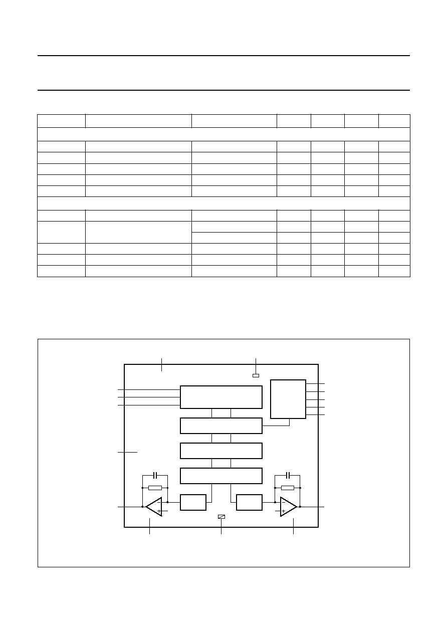
6
BLOCK DIAGRAM
7
PINNING
8
FUNCTIONAL DESCRIPTION
8.1
System clock
8.2
Application modes
8.3
Multiple format input interface
8.4
Static pin mode
8.5
Pin compatibility
8.6
Interpolation filter (DAC)
8.7
Noise shaper
8.8
Filter-Stream DAC
9
L3 INTERFACE DESCRIPTION
9.1
The L3 interface
9.2
Data transfer mode
9.3
Programming the features
10
LIMITING VALUES
11
HANDLING
12
QUALITY SPECIFICATION
13
THERMAL CHARACTERISTICS
14
DC CHARACTERISTICS
15
AC CHARACTERISTICS
15.1
Analog
15.2
Digital
16
APPLICATION INFORMATION
17
PACKAGE OUTLINE
18
SOLDERING
18.1
Introduction
18.2
Reflow soldering
18.3
Wave soldering
18.4
Repairing soldered joints
19
DEFINITIONS
20
LIFE SUPPORT APPLICATIONS
2000 Jan 10
3
Philips Semiconductors
Preliminary specification
Low-cost stereo filter DAC
UDA1320ATS
1
FEATURES
1.1
General
�
Low power consumption.
�
2.7 to 3.6 V power supply.
�
Selectable control via L3 microcontroller interface or via
static pin control.
�
256, 384 and 512f
s
system clock (f
sys
), selectable via
the L3 interface or 256 and 384f
s
clock mode via static
pin control
�
supports sampling frequencies from 16kHz to 48kHz.
�
Integrated digital filter plus non inverting DAC
Digital-to-Analog Converter (DAC).
�
Easy application and no analog post filtering required for
DAC.
�
Slave mode only applications.
�
Small package size (SSOP16).
1.2
Multiple format input interface
�
I
2
S-bus, MSB-justified and LSB-justified 16,18 and 20
bits format compatible (in L3-mode).
�
I
2
S-bus and LSB-justified 16,18 and 20 bits format
compatible in static mode.
�
1f
s
input format data rate.
1.3
DAC digital sound processing
�
Digital logarithmic volume control via L3.
�
Digital de-emphasis for 32, 44.1 and 48 kHz f
s
via
L3 or 44.1 kHz f
s
via static pin control.
�
Soft mute via static pin control or via L3 interface.
1.4
Advanced audio configuration
�
Stereo line output (under L3 volume control)
�
High linearity, wide dynamic range, low distortion.
2
APPLICATIONS
�
Portable digital audio equipment, see Fig.8.
�
Set-top boxes
3
GENERAL DESCRIPTION
The UDA1320ATS/N2 is a single-chip non inverting stereo
DAC employing bitstream conversion techniques. The low
power consumption and low voltage requirements make
the device eminently suitable for use in digital audio
equipment which incorporates playback functions.
The UDA1320ATS/N2 supports the I
2
S-bus data format
with word lengths of up to 20 bits, the MSB-justified data
format with word lengths of up to 20 bits and the
LSB-justified serial data format with word lengths of 16,
18 and 20 bits.
The UDA1320ATS/N2 can be used in two modes, either
L3-mode or static pin mode.
In the L3-mode, all digital sound processing features must
be controlled via the L3 interface, including the selection of
the system clock setting.
In the two static-modes, the UDA1320ATS/N2 can be
operated in the 256f
s
and 384f
s
system clock mode. The
mute, de-emphasis for 44.1 kHz and 4 digital input formats
(I
2
S and 16, 18, 20 bits LSB formats) can be selected via
static pins. The L3 interface cannot be used in this
application mode, also, volume control is not available in
this mode.
4
ORDERING INFORMATION
TYPE NUMBER
PACKAGE
NAME
DESCRIPTION
VERSION
UDA1320ATS
SSOP16
plastic shrink small outline package; 16 leads; body width 4.4 mm
SOT369-1
2000 Jan 10
5
Philips Semiconductors
Preliminary specification
Low-cost stereo filter DAC
UDA1320ATS
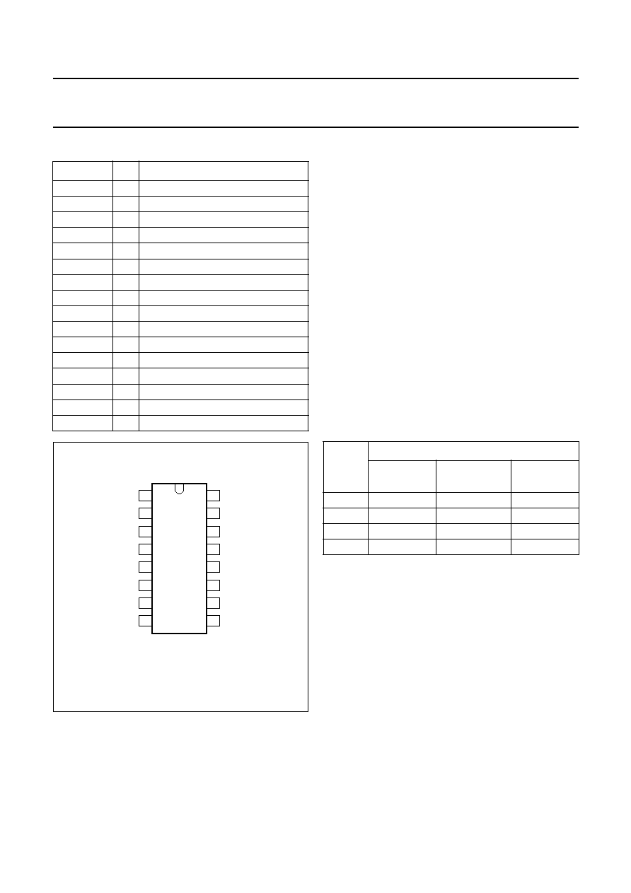
7
PINNING
8
FUNCTIONAL DESCRIPTION
8.1
System clock
The UDA1320ATS/N2 operates in slave mode only. This
means in all applications the system devices must provide
the system clock. The system frequency is selectable and
depends on the mode of operation.
The options are 256f
s
, 384f
s
and 512f
s
for the L3 mode
and 256f
s
plus 384f
s
for the static mode. The system clock
must be locked in frequency to the digital interface input
signals.
The UDA1320ATS/N2 supports sampling frequencies
from 16kHz up to 48kHz
8.2
Application modes
The application mode can be set with the tri-value
APPSEL pin, to L3 mode (APPSEL = V
SSD
) or to either of
two static modes (APPSEL = 0.5V
DDD
or
APPSEL = V
DDD
). See Table 1 for APPL0 to APPL3 pin
functions (active = HIGH).
Table 1
Selection modes via APPSEL (note 1)
For example, in static pin control mode, the output signal
can be soft muted by setting APPL0 HIGH. De-emphasis
can be switched on for 44.1 kHz by setting APPL1 HIGH.
APPL1 LOW will disable de-emphasis.
Note that when L3 interface is used, an L3 initialisation
must be done when the IC is powered up!
In L3 mode pin APPL0 must be set to LOW.
SYMBOL
PIN
DESCRIPTION
BCK
1
bit clock
WS
2
word select
DATAI
3
data input
V
DDD
4
digital power supply
V
SSD
5
digital ground
SYSCLK
6
system clock: 256f
s
, 384f
s
, 512f
s
APPSEL
7
application mode select
APPL3
8
application pin 3
APPL2
9
application pin 2
APPL1
10
application pin 1
APPL0
11
application pin 0
V
REF(DAC)
12
DAC reference voltage
V
DDA
13
analog supply voltage
V
O(L)
14
left output voltage
V
SSA
15
analog ground
V
O(R)
16
right output voltage
Fig.2 Pin configuration.
handbook, halfpage
UDA1320A
MGM817
1
2
3
4
5
6
7
8
16
15
14
13
12
11
10
9
VO(R)
BCK
VSSA
WS
VO(L)
DATAI
VDDA
VDDD
VREF(DAC)
VSSD
APPL0
SYSCLK
APPL1
APPSEL
APPL2
APPL3
PIN
APPSEL
V
SSD
0.5V
DDD
(384f
s
)
V
DDD
(256f
s
)
APPL0
TEST
MUTE
MUTE
APPL1
L3CLOCK
DEEM
DEEM
APPL2
L3MODE
SF0
SF0
APPL3
L3DATA
SF1
SF1