2002 May 16
2
Philips Semiconductors
Product specification
Economy audio CODEC for MiniDisc (MD)
home stereo and portable applications
UDA1341TS
CONTENTS
1
FEATURES
1.1
General
1.2
Multiple format data interface
1.3
DAC digital sound processing
1.4
Advanced audio configuration
2
GENERAL DESCRIPTION
3
ORDERING INFORMATION
4
QUICK REFERENCE DATA
5
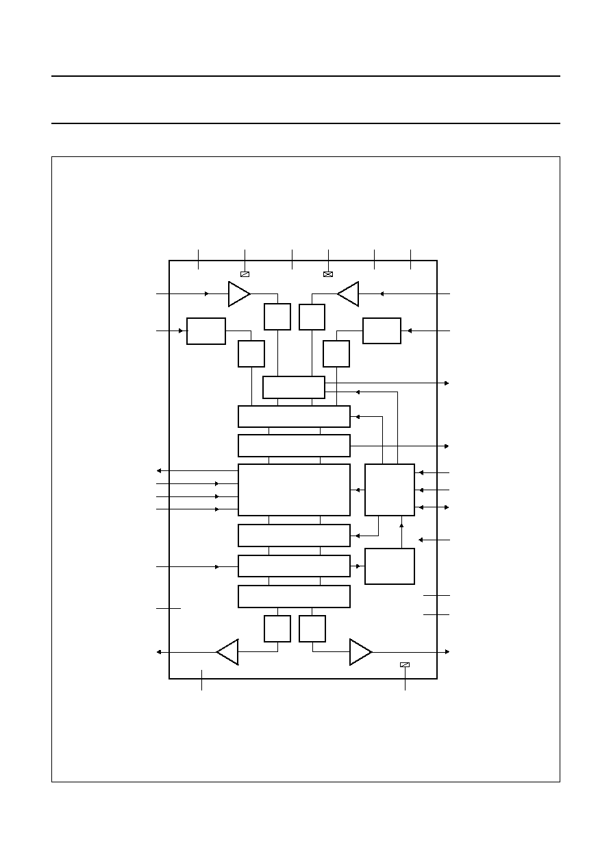
BLOCK DIAGRAM
6
PINNING
7
FUNCTIONAL DESCRIPTION
7.1
System clock
7.2
Pin compatibility
7.3
Analog front end
7.4
Programmable Gain Amplifier (PGA)
7.5
Analog-to-Digital Converter (ADC)
7.6
Digital Automatic Gain Control (AGC)
7.7
AGC status detection
7.8
Digital mixer
7.9
Decimation filter (ADC)
7.10
Overload detection (ADC)
7.11
Mute (ADC)
7.12
Interpolation filter (DAC)
7.13
Peak detector
7.14
Quick mute
7.15
Noise shaper (DAC)
7.16
Filter Stream Digital-to-Analog Converter
(FSDAC)
7.17
Multiple format input/output interface
7.18
L3-interface
7.19
Address mode
7.20
Data transfer mode
7.21
Programming the sound processing and other
features
7.21.1
STATUS control
7.21.2
DATA0 direct control
7.21.3
DATA0 extended programming registers
7.21.4
DATA1 control
8
LIMITING VALUES
9
THERMAL CHARACTERISTICS
10
DC CHARACTERISTICS
11
AC CHARACTERISTICS (ANALOG)
12
AC CHARACTERISTICS (DIGITAL)
13
APPLICATION INFORMATION
14
PACKAGE OUTLINE
15
SOLDERING
15.1
Introduction to soldering surface mount
packages
15.2
Reflow soldering
15.3
Wave soldering
15.4
Manual soldering
15.5
Suitability of surface mount IC packages for
wave and reflow soldering methods
16
DATA SHEET STATUS
17
DEFINITIONS
18
DISCLAIMERS
2002 May 16
3
Philips Semiconductors
Product specification
Economy audio CODEC for MiniDisc (MD)
home stereo and portable applications
UDA1341TS
1
FEATURES
1.1
General
�
Low power consumption
�
3.0 V power supply
�
256f
s
, 384f
s
or 512f
s
system clock frequencies (f
sys
)
�
Small package size (SSOP28)
�
Partially pin compatible with UDA1340M and
UDA1344TS
�
Fully integrated analog front end including digital AGC
�
ADC plus integrated high-pass filter to cancel DC offset
�
ADC supports 2 V (RMS value) input signals
�
Overload detector for easy record level control
�
Separate power control for ADC and DAC
�
No analog post filter required for DAC
�
Easy application
�
Functions controllable via L3-interface.
1.2
Multiple format data interface
�
I
2
S-bus, MSB-justified and LSB-justified format
compatible
�
Three combinational data formats with MSB data output
and LSB 16, 18 or 20 bits data input
�
1f
s
input and output format data rate.
1.3
DAC digital sound processing
�
Digital dB-linear volume control (low microcontroller
load)
�
Digital tone control, bass boost and treble
�
Digital de-emphasis for 32, 44.1 or 48 kHz audio sample
frequencies (f
s
)
�
Soft mute.
1.4
Advanced audio configuration
�
DAC and ADC polarity control
�
Two channel stereo single-ended input configuration
�
Microphone input with on-board PGA
�
Optional differential input configuration for enhanced
ADC sound quality
�
Stereo line output (under microcontroller volume
control)
�
Digital peak level detection
�
High linearity, dynamic range and low distortion.
2
GENERAL DESCRIPTION
The UDA1341TS is a single-chip stereo Analog-to-Digital
Converter (ADC) and Digital-to-Analog Converter (DAC)
with signal processing features employing bitstream
conversion techniques. Its fully integrated analog front
end, including Programmable Gain Amplifier (PGA) and a
digital Automatic Gain Control (AGC). Digital Sound
Processing (DSP) featuring makes the device an excellent
choice for primary home stereo MiniDisc applications, but
by virtue of its low power and low voltage characteristics it
is also suitable for portable applications such as MD/CD
boomboxes, notebook PCs and digital video cameras.
The UDA1341TS is similar to the UDA1340M and the
UDA1344TS but adds features such as digital mixing of
two input signals and one channel with a PGA and a digital
AGC.
The UDA1341TS supports the I
2
S-bus data format with
word lengths of up to 20 bits, the MSB-justified data format
with word lengths of up to 20 bits, the LSB-justified serial
data format with word lengths of 16, 18 and 20 bits and
three combinations of MSB data output combined with
LSB 16, 18 and 20 bits data input. The UDA1341TS has
DSP features in playback mode like de-emphasis, volume,
bass boost, treble and soft mute, which can be controlled
via the L3-interface with a microcontroller.
3
ORDERING INFORMATION
TYPE
NUMBER
PACKAGE
NAME
DESCRIPTION
VERSION
UDA1341TS
SSOP28
plastic shrink small outline package; 28 leads; body width 5.3 mm
SOT341-1
2002 May 16
4
Philips Semiconductors
Product specification
Economy audio CODEC for MiniDisc (MD)
home stereo and portable applications
UDA1341TS
4
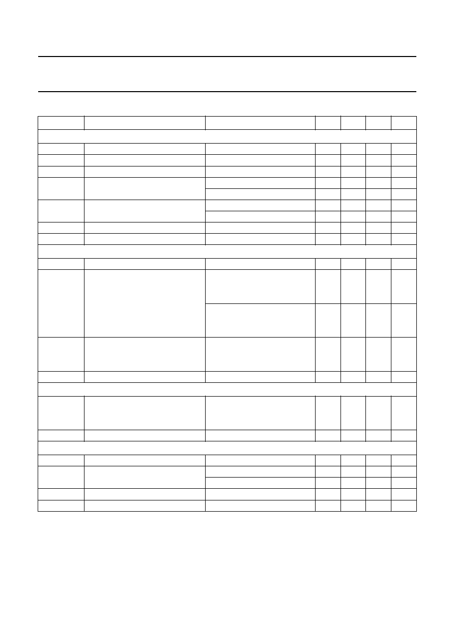
QUICK REFERENCE DATA
Notes
1. The ADC inputs can be used in a 2 V (RMS value) input signal configuration when a resistor of 12 k
is used in series
with the inputs and 1 or 2 V (RMS value) input signal operation can be selected via the Input Gain Switch (IGS).
2. The ADC input signal scales inversely proportional with the power supply voltage.
3. The DAC output voltage scales linear with the DAC analog supply voltage.
SYMBOL
PARAMETER
CONDITIONS
MIN.
TYP.
MAX.
UNIT
Supplies
V
DDA(ADC)
ADC analog supply voltage
2.4
3.0
3.6
V
V
DDA(DAC)
DAC analog supply voltage
2.4
3.0
3.6
V
V
DDD
digital supply voltage
2.4
3.0
3.6
V
I
DDA(ADC)
ADC analog supply current
operation mode
-
12.5
-
mA
ADC power-down
-
6.0
-
mA
I
DDA(DAC)
DAC analog supply current
operation mode
-
7.0
-
mA
DAC power-down
-
50
-
�
A
I
DDD
digital supply current
operation mode
-
7.0
-
mA
T
amb
operating ambient temperature
-
20
-
+85
�
C
Analog-to-digital converter
V
i(rms)
input voltage (RMS value)
notes 1 and 2
-
1.0
-
V
(THD + N)/S total harmonic distortion-plus-noise
to signal ratio
stand-alone mode
0 dB
-
-
85
-
80
dB
-
60 dB; A-weighted
-
-
37
-
33
dB
double differential mode
0 dB
-
-
90
-
85
dB
-
60 dB; A-weighted
-
-
40
-
36
dB
S/N
signal-to-noise ratio
V
i
= 0 V; A-weighted
stand-alone mode
-
97
-
dB
double differential mode
-
100
-
dB
cs
channel separation
-
100
-
dB
Programmable gain amplifier
(THD + N)/S total harmonic distortion-plus-noise
to signal ratio
1 kHz; f
s
= 44.1 kHz
0 dB
-
-
85
-
dB
-
60 dB; A-weighted
-
-
37
-
dB
S/N
signal-to-noise ratio
V
i
= 0 V; A-weighted
-
95
-
dB
Digital-to-analog converter
V
o(rms)
output voltage (RMS value)
supply voltage = 3 V; note 3
-
900
-
mV
(THD+N)/S
total harmonic distortion-plus-noise
to signal ratio
0 dB
-
-
91
-
86
dB
-
60 dB; A-weighted
-
-
40
-
dB
S/N
signal-to-noise ratio
code = 0; A-weighted
-
100
-
dB
cs
channel separation
-
100
-
dB