2000 Apr 18
2
Philips Semiconductors
Preliminary specification
Economy audio CODEC
UDA1345TS
FEATURES
General
∑
Low power consumption
∑
2.4 V to 3.6 V power supply range with 3.0 V typical
∑
5 V tolerant TTL compatible digital inputs
∑
256, 384 and 512f
s
system clock
∑
Supports sampling frequencies from 8 to 100 kHz
∑
Non-inverting ADC plus integrated high-pass filter to
cancel DC offset
∑
The ADC supports 2 V (RMS) input signals
∑
Overload detector for easy record level control
∑
Separate power control for ADC and DAC
∑
Integrated digital interpolation filter plus non-inverting
DAC
∑
Functions controllable either by L3 microcontroller
interface or via static pins
∑
The UDA1345TS is pin and function compatible with the
UDA1344TS
∑
Small package size (SSOP28).
Multiple format input interface
∑
I
2
S-bus, MSB-justified up to 24 bits and LSB-justified
16, 18 and 20 bits format compatible
∑
Three combined data formats with MSB data output and
LSB 16, 18 and 20 bits data input
∑
1f
s
input and output format data rate.
DAC digital sound processing
The sound processing features of the UDA1345TS can
only be used in L3 microcontroller mode:
∑
Digital dB-linear volume control (low microcontroller
load) via L3 microcontroller with 1 dB steps
∑
Digital de-emphasis for 32, 44.1 and 48 kHz
∑
Soft mute via cosine roll-off (in 1024 samples).
Note: in contrast to the UDA1344TS, the UDA1345TS
does not have bass-boost and treble.
Advanced audio configuration
∑
Stereo single-ended input configuration
∑
Stereo line output (under microcontroller volume
control), no post filter required
∑
High linearity, dynamic range and low distortion.
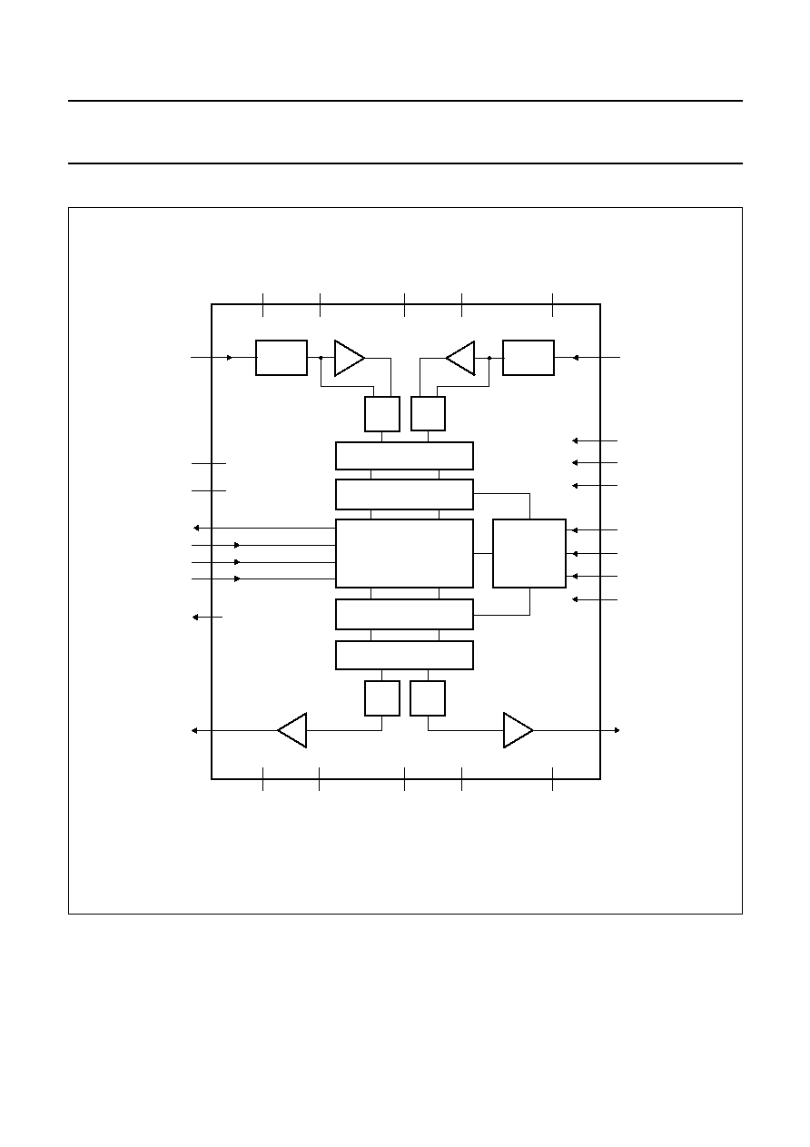
GENERAL DESCRIPTION
The UDA1345TS is a single-chip stereo Analog-to-Digital
Converter (ADC) and Digital-to-Analog Converter (DAC)
with signal processing features employing bitstream
conversion techniques. The low power consumption and
low voltage requirements make the device eminently
suitable for use in low-voltage low-power portable digital
audio equipment which incorporates recording and
playback functions.
The UDA1345TS supports the I
2
S-bus data format with
word lengths of up to 24 bits, the MSB justified data format
with word lengths of up to 20 bits and the LSB justified
serial data format with word lengths of 16, 18 and 20 bits.
The UDA1345TS also supports three combined data
formats with MSB justified data output and LSB 16, 18
and 20 bits data input.
The UDA1345TS can be used either with static pin control
or under L3 microcontroller interface. In L3 mode the
UDA1345TS has basic sound features in playback mode
such as de-emphasis, volume control and soft mute.
ORDERING INFORMATION
TYPE NUMBER
PACKAGE
NAME
DESCRIPTION
VERSION
UDA1345TS
SSOP28
plastic shrink small outline package; 28 leads; body width 5.3 mm
SOT341-1
2000 Apr 18
3
Philips Semiconductors
Preliminary specification
Economy audio CODEC
UDA1345TS
QUICK REFERENCE DATA
SYMBOL
PARAMETER
CONDITIONS
MIN.
TYP.
MAX.
UNIT
Supplies
V
DDA(ADC)
ADC analog supply voltage
2.4
3.0
3.6
V
V
DDA(DAC)
DAC analog supply voltage
2.4
3.0
3.6
V
V
DDD
digital supply voltage
2.4
3.0
3.6
V
I
DDA(ADC)
ADC analog supply current
operating mode
-
10
-
mA
ADC power-down
-
100
-
µ
A
I
DDA(DAC)
DAC analog supply current
operating mode
-
4
-
mA
DAC power-down
-
50
-
µ
A
I
DDO(DAC)
DAC operational amplifier supply
current
operating mode
-
2.5
-
mA
DAC power-down
-
200
-
µ
A
I
DDD
digital supply current
operating mode
-
5
-
mA
ADC and DAC power-down
-
300
-
µ
A
T
amb
ambient temperature
-
40
-
+85
∞
C
Analog-to-digital converter
V
i(rms)
input voltage (RMS value)
notes 1 and 2
-
1.0
-
V
(THD + N)/S
total harmonic distortion-plus-noise
to signal ratio
at 0 dB
f
s
= 44.1 kHz
-
-
85
-
80
dB
f
s
= 96 kHz
-
-
80
-
75
dB
at
-
60 dB; A-weighted
f
s
= 44.1 kHz
-
-
36
-
30
dB
f
s
= 96 kHz
-
-
34
-
30
dB
S/N
signal-to-noise ratio
V
i
= 0 V; A-weighted
f
s
= 44.1 kHz
90
96
-
dB
f
s
= 96 kHz
90
94
-
dB
cs
channel separation
-
100
-
dB
Digital-to-analog converter
V
o(rms)
output voltage (RMS value)
note 3
-
900
-
mV
(THD + N)/S
total harmonic distortion plus
noise-to-signal ratio
at 0 dB
f
s
= 44.1 kHz
-
-
85
-
80
dB
f
s
= 96 kHz
-
-
80
-
71
dB
at
-
60 dB; A-weighted
f
s
= 44.1 kHz
-
-
37
-
30
dB
f
s
= 96 kHz
-
-
35
-
30
dB
cs
channel separation
-
100
-
dB
S/N
signal-to-noise ratio
code = 0; A-weighted
f
s
= 44.1 kHz
90
100
-
dB
f
s
= 96 kHz
90
98
-
dB
2000 Apr 18
4
Philips Semiconductors
Preliminary specification
Economy audio CODEC
UDA1345TS
Notes
1. The input voltage can be up to 2 V (RMS) when the current through the ADC input pin is limited to approximately
1 mA by using a series resistor.
2. The input voltage to the ADC scales proportionally with the power supply voltage.
3. The output voltage of the DAC scales proportionally with the power supply voltage.
Power performance
P
ADDA
power consumption in record and
playback mode
-
64
-
mW
P
DA
power consumption in playback only
mode
-
36
-
mW
P
AD
power consumption in record only
mode
-
46
-
mW
P
PD
power consumption in power-down
mode
-
2.0
-
mW
SYMBOL
PARAMETER
CONDITIONS
MIN.
TYP.
MAX.
UNIT