
1.
General description
The UDA1384 is a single-chip consisting of 4 plus 1 Analog-to-Digital Converters (ADC)
and 6 Digital-to-Analog Converters (DAC) with signal processing features employing
bitstream conversion techniques. The multichannel configuration makes the device
eminently suitable for use in digital audio equipment which incorporates surround feature.
The UDA1384 supports conventional 2 channels per line data transfer conformable to the
I
2
S-bus format with word lengths of up to 24 bits, the MSB-justified format with word
lengths of up to 24 bits and the LSB-justified format with word lengths of 16 bits, 20 bits
and 24 bits, as well as 4 channels to 6 channels per line transfer mode. The device also
supports a combination of the MSB-justified output format and the LSB-justified input
format. The UDA1384 has special sound processing features in the Direct Stream Digital
(DSD) playback mode, de-emphasis, volume and mute which can be controlled via the
L3-bus or I
2
C-bus interface.
2.
Features
2.1 General
s
2.7 V to 3.6 V power supply
s
5 V tolerant digital inputs
s
24-bit data path
s
Selectable control: via L3-bus or I
2
C-bus microcontroller interface
s
Supports sample frequency ranges for:
x
Audio ADC: f
s
= 16 kHz to 100 kHz
x
Voice ADC: f
s
= 7 kHz to 50 kHz
x
Audio DAC: f
s
= 16 kHz to 200 kHz
s
Separate power control for ADC and DAC
s
ADC plus integrated high-pass filter to cancel DC offset
s
Integrated digital filter plus DAC
s
Slave mode only applications
s
Easy application
UDA1384
Multichannel audio coder-decoder
Rev. 02 -- 17 January 2005
Product data sheet

9397 750 14366
� Koninklijke Philips Electronics N.V. 2005. All rights reserved.
Product data sheet
Rev. 02 -- 17 January 2005
2 of 55
Philips Semiconductors
UDA1384
Multichannel audio coder-decoder
2.2 Multiple format data interface
s
Audio interface supports standard I
2
S-bus, MSB-justified, LSB-justified and two
multichannel formats
s
Voice interface supports I
2
S-bus and mono channel formats
2.3 Digital sound processing
s
Control via L3-bus or I
2
C-bus:
x
Channel independent digital logarithmic volume
x
Digital de-emphasis for f
s
= 32 kHz, 44.1 kHz, 48 kHz or 96 kHz
x
Soft or quick mute
x
Output signal polarity control
2.4 Advanced audio configuration
s
Inputs:
x
4 single-ended audio inputs (2
�
stereo) with programmable gain amplifiers
x
1 single-ended voice input
s
Outputs:
x
6 differential audio outputs (3
�
stereo)
s
DSD mode to support stereo DSD playback
s
High linearity, wide dynamic range and low distortion
s
DAC digital filter with selectable sharp or soft roll-off
3.
Applications
s
Excellently suitable for multichannel home audio-video application
4.
Quick reference data
Table 1:
Quick reference data
V
DDD
= V
DDA(AD)
= V
DDA(DA)
= 3.3 V; T
amb
= 25
�
C; R
L
= 22 k
; all voltages referenced to ground
(pins V
SS
); unless otherwise specified.
Symbol
Parameter
Conditions
Min
Typ
Max
Unit
Supplies
V
DDA(AD)
ADC analog supply
voltage
2.7
3.3
3.6
V
V
DDA(DA)
DAC analog supply
voltage
2.7
3.3
3.6
V
V
DDD
digital supply voltage
2.7
3.3
3.6
V
I
DDA(AD)
ADC analog supply
current
f
ADC
= 48 kHz
-
30
-
mA
I
DDA(DA)
DAC analog supply
current
f
DAC
= 48 kHz
-
20
-
mA
I
DDD
digital supply current f
ADC
= f
DAC
= 48 kHz;
f
VOICE
= 48 kHz
-
31
-
mA

9397 750 14366
� Koninklijke Philips Electronics N.V. 2005. All rights reserved.
Product data sheet
Rev. 02 -- 17 January 2005
3 of 55
Philips Semiconductors
UDA1384
Multichannel audio coder-decoder
[1]
The input voltage can be up to 2 V (RMS) when the current through the ADC input pin is limited to
approximately 1 mA by using a series resistor.
[2]
The input voltage to the ADC scales proportionally with the power supply voltage.
5.
Ordering information
I
DDD(pd)
digital supply current
in Power-down mode
audio and voice
ADCs power-down
-
18
-
mA
DAC power-down
-
14
-
mA
T
amb
ambient temperature
-
20
-
+85
�
C
Audio analog-to-digital converter
D
0
digital output level
at 0 dB setting;
900 mV input
[1] [2]
-
2.5
-
1.2
-
0.7
dB
(THD+N)/S
total harmonic
distortion-plus-noise
to signal ratio
at
-
1 dBFS
-
-
88
-
82
dB
at
-
60 dBFS;
A-weighted
-
-
37
-
30
dB
S/N
signal-to-noise ratio
code = 0; A-weighted
89
98
-
dB
cs
channel separation
-
100
-
dB
Digital-to-analog converter
Differential mode
V
o(rms)
output voltage
(RMS value)
at 0 dBFS digital
input
1.9
2.0
2.1
V
(THD+N)/S
total harmonic
distortion-plus-noise
to signal ratio
at 0 dBFS
-
-
98
-
89
dB
at
-
60 dBFS;
A-weighted
-
-
50
-
45
dB
S/N
signal-to-noise ratio
code = 0; A-weighted
100
110
-
dB
cs
channel separation
-
114
-
dB
Single-ended mode
V
o(rms)
output voltage
(RMS value)
at 0 dBFS digital
input
-
1.0
-
V
(THD+N)/S
total harmonic
distortion-plus-noise
to signal ratio
at 0 dBFS
-
-
88
-
dB
at
-
60 dBFS;
A-weighted
-
-
45
-
dB
S/N
signal-to-noise ratio
code = 0; A-weighted
-
105
-
dB
cs
channel separation
-
110
-
dB
Table 1:
Quick reference data
...continued
V
DDD
= V
DDA(AD)
= V
DDA(DA)
= 3.3 V; T
amb
= 25
�
C; R
L
= 22 k
; all voltages referenced to ground
(pins V
SS
); unless otherwise specified.
Symbol
Parameter
Conditions
Min
Typ
Max
Unit
Table 2:
Ordering information
Type number
Package
Name
Description
Version
UDA1384H
QFP44
plastic quad flat package; 44 leads (lead length
1.3 mm); body 10
�
10
�
1.75 mm
SOT307-2

9397 750 14366
� Koninklijke Philips Electronics N.V. 2005. All rights reserved.
Product data sheet
Rev. 02 -- 17 January 2005
4 of 55
Philips Semiconductors
UDA1384
Multichannel audio coder-decoder
6.
Block diagram
Fig 1.
Block diagram
mce639
PGA
ADC 2L
PLL
PLL
I
2
S-BUS
INTERFACE 3
HP FILTER
DECIMATION
FILTER
6
21
20
22
30
37
40
24
23
VINL2
MCCLK
MCMODE
MCDATA
I2C_L3
BCKDA
WSDA
5
3
DECIMATION FILTER
DC-CANCELLATION FILTER
I
2
S-BUS
INTERFACE 2
L3-BUS OR
I
2
C-BUS
CONTROL
INTERFACE
V
DDA(DA)
V
SSA(DA)
INTERPOLATION FILTER
VOLUME, MUTE, DE-EMPHASIS
NOISE SHAPER
I
2
S-BUS
INTERFACE 1
V
DDA(AD)
9
V
ADCP
7
V
ADCN
1
V
ref
V
SSA(AD)
UDA1384
LNA
10
VVOICE
PGA
ADC 1L
PGA
ADC 2R
PGA
ADC 1R
2
VINL1
VOUT2N
VOUT2P
VOUT4N
VOUT4P
VOUT6N
VOUT6P
VOUT1N
VOUT1P
VOUT3N
VOUT3P
VOUT5N
VOUT5P
DAC 2
34
-
+
33
39
38
44
43
32
31
36
35
42
41
DAC 4
-
+
DAC 6
DAC 1
DAC 3
DAC 5
-
+
-
+
ADC
CLOCK
TEST
-
+
-
+
25
DATADA1
26
DATADA2
27
DATADA3
13
DATAAD1
12
DATAAD2
14
BCKAD
11
TEST
4
VINR1
8
VINR2
19
SYSCLK
15
WSAD
17
BCKV
16
DATAV
18
WSV
28
29
V
DDD
V
SSD

9397 750 14366
� Koninklijke Philips Electronics N.V. 2005. All rights reserved.
Product data sheet
Rev. 02 -- 17 January 2005
5 of 55
Philips Semiconductors
UDA1384
Multichannel audio coder-decoder
7.
Pinning information
7.1 Pinning
7.2 Pin description
Fig 2.
Pin configuration
UDA1384H
V
ref
VOUT2P
VINL1
VOUT1N
V
SSA(AD)
VOUT1P
VINR1
I2C_L3
V
DDA(AD)
V
DDD
VINL2
V
SSD
V
ADCN
DATADA3
VINR2
DATADA2
V
ADCP
DATADA1
VVOICE
BCKDA
TEST
WSDA
DATAAD2
VOUT6N
DATAAD1
VOUT6P
BCKAD
VOUT5N
WSAD
VOUT5P
DATAV
V
SSA(D
A)
BCKV
VOUT4N
WSV
VOUT4P
SYSCLK
V
DD
A(D
A)
MCMODE
VOUT3N
MCCLK
VOUT3P
MCDATA
VOUT2N
001aac311
1
2
3
4
5
6
7
8
9
10
11
33
32
31
30
29
28
27
26
25
24
23
12
13
14
15
16
17
18
19
20
21
22
44
43
42
41
40
39
38
37
36
35
34
Table 3:
Pin description
Symbol
Pin
Type
Description
V
ref
1
AIO
ADC reference voltage
VINL1
2
AIO
ADC 1 input left
V
SSA(AD)
3
AGND
ADC analog ground
VINR1
4
AIO
ADC 1 input right
V
DDA(AD)
5
AS
ADC analog supply voltage
VINL2
6
AIO
ADC 2 input left
V
ADCN
7
AIO
ADC reference voltage N
VINR2
8
AIO
ADC 2 input right
V
ADCP
9
AIO
ADC reference voltage P
VVOICE
10
AIO
voice ADC input
TEST
11
DID
test input; must be connected to digital ground (V
SSD
) in
application
DATAAD2
12
DO
ADC 2 data output
DATAAD1
13
DO
ADC 1 data output
BCKAD
14
DIS
ADC bit clock input
WSAD
15
DI
ADC word select input

9397 750 14366
� Koninklijke Philips Electronics N.V. 2005. All rights reserved.
Product data sheet
Rev. 02 -- 17 January 2005
6 of 55
Philips Semiconductors
UDA1384
Multichannel audio coder-decoder
[1]
See
Table 4
.
DATAV
16
DO
voice data output
BCKV
17
DIS
voice bit clock input
WSV
18
DIO
voice word select input or output
SYSCLK
19
DIS
system clock input: 256f
s
, 384f
s
, 512f
s
or 768f
s
MCMODE
20
DI
L3-bus L3MODE input or I
2
C-bus DAC mute control input
MCCLK
21
DIS
L3-bus L3CLOCK input or I
2
C-bus SCL input
MCDATA
22
IIC
L3-bus L3DATA input and output or I
2
C-bus SDA input and
output
WSDA
23
DI
DAC word select input
BCKDA
24
DIS
DAC bit clock input
DATADA1
25
DI
DAC channel 1 and channel 2 data input
DATADA2
26
DI
DAC channel 3 and channel 4 data input
DATADA3
27
DI
DAC channel 5 and channel 6 data input
V
SSD
28
DGND
digital ground
V
DDD
29
DS
digital supply voltage
I2C_L3
30
DI
selection input for L3-bus or I
2
C-bus control
VOUT1P
31
AIO
DAC 1 positive output
VOUT1N
32
AIO
DAC 1 negative output
VOUT2P
33
AIO
DAC 2 positive output
VOUT2N
34
AIO
DAC 2 negative output
VOUT3P
35
AIO
DAC 3 positive output
VOUT3N
36
AIO
DAC 3 negative output
V
DDA(DA)
37
AS
DAC analog supply voltage
VOUT4P
38
AIO
DAC 4 positive output
VOUT4N
39
AIO
DAC 4 negative output
V
SSA(DA)
40
AGND
DAC analog ground
VOUT5P
41
AIO
DAC 5 positive output
VOUT5N
42
AIO
DAC 5 negative output
VOUT6P
43
AIO
DAC 6 positive output
VOUT6N
44
AIO
DAC 6 negative output
Table 4:
Pin types
Type
Description
AGND
analog ground
AIO
analog input and output
AS
analog supply
DGND
digital ground
DI
digital input
DID
digital input with internal pull-down resistor
DIO
digital input and output
Table 3:
Pin description
...continued
Symbol
Pin
Type
Description

9397 750 14366
� Koninklijke Philips Electronics N.V. 2005. All rights reserved.
Product data sheet
Rev. 02 -- 17 January 2005
7 of 55
Philips Semiconductors
UDA1384
Multichannel audio coder-decoder
8.
Functional description
8.1 System clock
The UDA1384 operates in slave mode only; this means that in all applications the system
must provide either the system clock (the bit clock for the voice ADC) or the word clock.
The audio ADC part, the voice ADC part and the DAC part can operate at different
sampling frequencies (DAC-WS and ADC-WS modes) as well as a common frequency
(SYSCLK, WSDA and DSD modes).
The voice ADC part supports a sampling frequency up to 50 kHz and the audio ADC
supports a sampling frequency up to 100 kHz. The DAC sampling frequency range is
extended up to 200 kHz with the range above 100 kHz being supported through 192 kHz
sampling mode, which halves the oversampling ratio of SYSCLK and internal clocks.
The mode of operation of the audio and voice channels can be set via the L3-bus or
I
2
C-bus microcontroller interface and are summarized in
Table 5
and
Table 6
.
When applied, the system clock must be locked in frequency to the corresponding digital
interface clocks.
The voice ADC part can either receive or generate the WSV signal as shown in
Table 6
.
DIS
digital Schmitt-triggered input
DO
digital output
DS
digital supply
IIC
input and open-drain output for I
2
C-bus
Table 4:
Pin types
...continued
Type
Description
Table 5:
Audio ADC and DAC operating clock mode
Mode
Audio ADC
Audio DAC
Clock
Frequency
Clock
Frequency
SYSCLK
SYSCLK
256f
s
, 384f
s
, 512f
s
or 768f
s
SYSCLK
256f
s
, 384f
s
, 512f
s
or 768f
s
SYSCLK
128f
s
, 192f
s
, 256f
s
or 384f
s
;
192 kHz sampling mode
DAC-WS
SYSCLK
256f
s
, 384f
s
, 512f
s
or 768f
s
WSDA
1f
s
ADC-WS
WSAD
1f
s
SYSCLK
256f
s
, 384f
s
, 512f
s
or 768f
s
SYSCLK
128f
s
, 192f
s
, 256f
s
or 384f
s
;
192 kHz sampling mode
WSDA
WSDA
1f
s
WSDA
1f
s
DSD
SYSCLK
44.1 kHz
�
512
SYSCLK
44.1 kHz
�
512
Table 6:
Voice ADC operating clock mode
Mode
Voice ADC
Bit clock frequency (BCKV)
Word select (WSV)
WSV-in
input: 32f
s
, 64f
s
, 128f
s
or 256f
s
input
WSV-out
input: 32f
s
, 64f
s
, 128f
s
or 256f
s
output
9397 750 14366
� Koninklijke Philips Electronics N.V. 2005. All rights reserved.
Product data sheet
Rev. 02 -- 17 January 2005
8 of 55
Philips Semiconductors
UDA1384
Multichannel audio coder-decoder
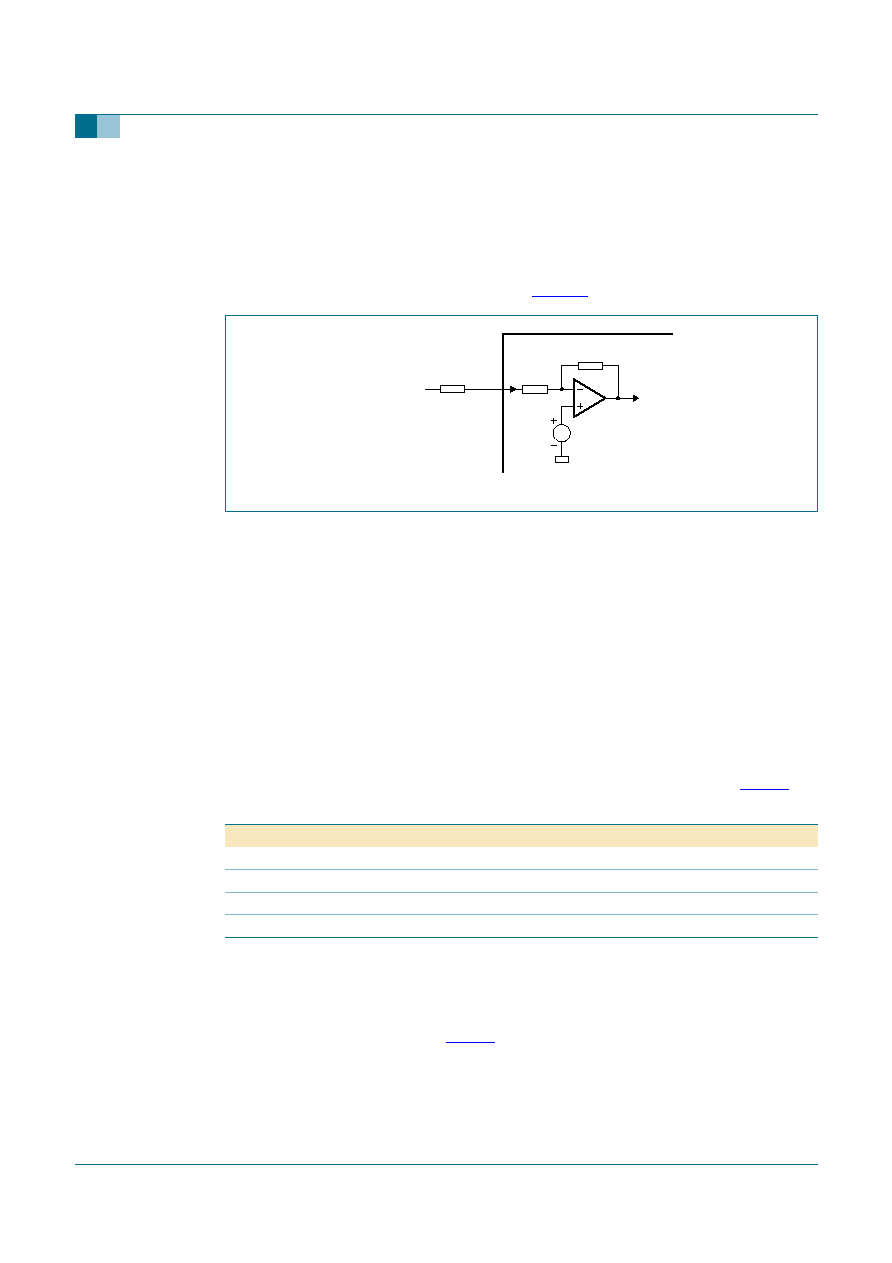
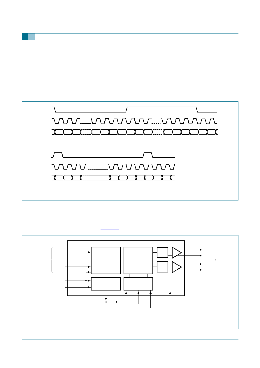
8.2 Audio analog-to-digital converter (audio ADC)
The audio analog-to-digital front-end of the UDA1384 consists of 4-channel single-ended
ADCs with programmable gain stage (from 0 dB to 24 dB with 3 dB steps), controlled via
the microcontroller interface. Using the PGA feature, it is possible to accept an input signal
of 900 mV (RMS) or 1.8 V (RMS) if an external resistor of 10 k
is used in series. The
schematic of audio ADC front-end is shown in
Figure 3
.
8.3 Voice Analog-to-Digital Converter (voice ADC)
The voice analog-to-digital front-end of the UDA1384 consists of a single-channel
single-ended ADC with a fixed gain (26 dB) Low Noise Amplifier (LNA). Together with the
digital variable gain amplification stage, the voice ADC provides optimal processing and
reproduction of the microphone signal. The supported sampling frequency range is from
7 kHz to 50 kHz. Power-down of the LNA and the ADC can be controlled separately.
8.4 Decimation filter of audio ADC
The decimation from 64f
s
is performed in two stages. The first stage realizes
characteristics with a decimation factor of 8. The second stage consists of three half-band
filters, each decimating by a factor of 2. The filter characteristics are shown in
Table 7
.
8.5 Decimation filter of voice ADC
The voice ADC decimation filter is realized with the combination of a Finite Impulse
Response (FIR) filter and Infinite Impulse Response (IIR) filter for shorter group delay. The
filter characteristics are shown in
Table 8
. During the power-on sequence, the output of
the ADC is hard muted for a certain period. This hard-mute time can be chosen between
1024 samples and 2048 samples.
Fig 3.
Schematic of audio ADC front-end
mgu582
V
ref
ADC
V
DDA
= 3.3 V
VINL,
VINR
10 k
(0 dB setting)
10 k
10 k
input signal
2 V (RMS)
Table 7:
Decimation filter characteristics (audio ADC)
Item
Condition
Value (dB)
Pass-band ripple
0f
s
to 0.45f
s
�
0.01
Pass-band droop
0.45f
s
-
0.2
Stop band
> 0.55f
s
-
70
Dynamic range
0f
s
to 0.45f
s
> 135
x
sin
x
----------
4

9397 750 14366
� Koninklijke Philips Electronics N.V. 2005. All rights reserved.
Product data sheet
Rev. 02 -- 17 January 2005
9 of 55
Philips Semiconductors
UDA1384
Multichannel audio coder-decoder
8.6 Interpolation filter of DAC
The digital interpolation filter interpolates from 1f
s
to 128f
s
(or to 64f
s
in the 192 kHz
sampling mode) by cascading FIR filters, and has two sets of filter coefficients for sharp
and slow roll-off as given in
Table 9
and
Table 10
.
8.7 Noise shaper of DAC
The 3rd-order noise shaper operates at either 128f
s
or 64f
s
(in the 192 kHz sampling
mode), and converts the 24-bit input signal into a 5-bit signal stream. The noise shaper
shifts in-band quantization noise to frequencies well above the audio band. This noise
shaping technique enables high signal-to-noise ratios to be achieved.
8.8 Digital mixer
The UDA1384 has 6 digital mixers inside the interpolator (see
Figure 4
). The ADC signals
can be mixed with the I
2
S-bus input signals. The mixing of the ADC signals can be
selected by the bits MIX[1:0].
Table 8:
Decimation filter characteristics (voice ADC)
Item
Condition
Value (dB)
Pass-band ripple
0f
s
to 0.45f
s
�
0.05
Pass-band droop
0.45f
s
-
0.2
Stop band
> 0.55f
s
-
65
Dynamic range
0f
s
to 0.45f
s
> 110
Table 9:
Interpolation filter characteristics (sharp roll-off)
Item
Condition
Value (dB)
Pass-band ripple
0f
s
to 0.45f
s
�
0.002
Stop band
> 0.55f
s
-
75
Dynamic range
0f
s
to 0.45f
s
> 135
Table 10:
Interpolation filter characteristics (slow roll-off)
Item
Condition
Value (dB)
Pass-band ripple
0f
s
to 0.22f
s
�
0.002
Pass-band droop
0.45f
s
-
3.1
Stop band
> 0.78f
s
-
94
Dynamic range
0f
s
to 0.22f
s
> 135

9397 750 14366
� Koninklijke Philips Electronics N.V. 2005. All rights reserved.
Product data sheet
Rev. 02 -- 17 January 2005
10 of 55
Philips Semiconductors
UDA1384
Multichannel audio coder-decoder
8.9 Audio digital-to-analog converters
The audio digital-to-analog front-end of the UDA1384 consists of 6-channel differential
SDACs: an SDAC is a multi-bit DAC based upon switched resistors. To minimize data
dependent modulation effects, a Dynamic Element Matching (DEM) algorithm scrambler
circuit and DC current compensation circuit are implemented with the SDAC.
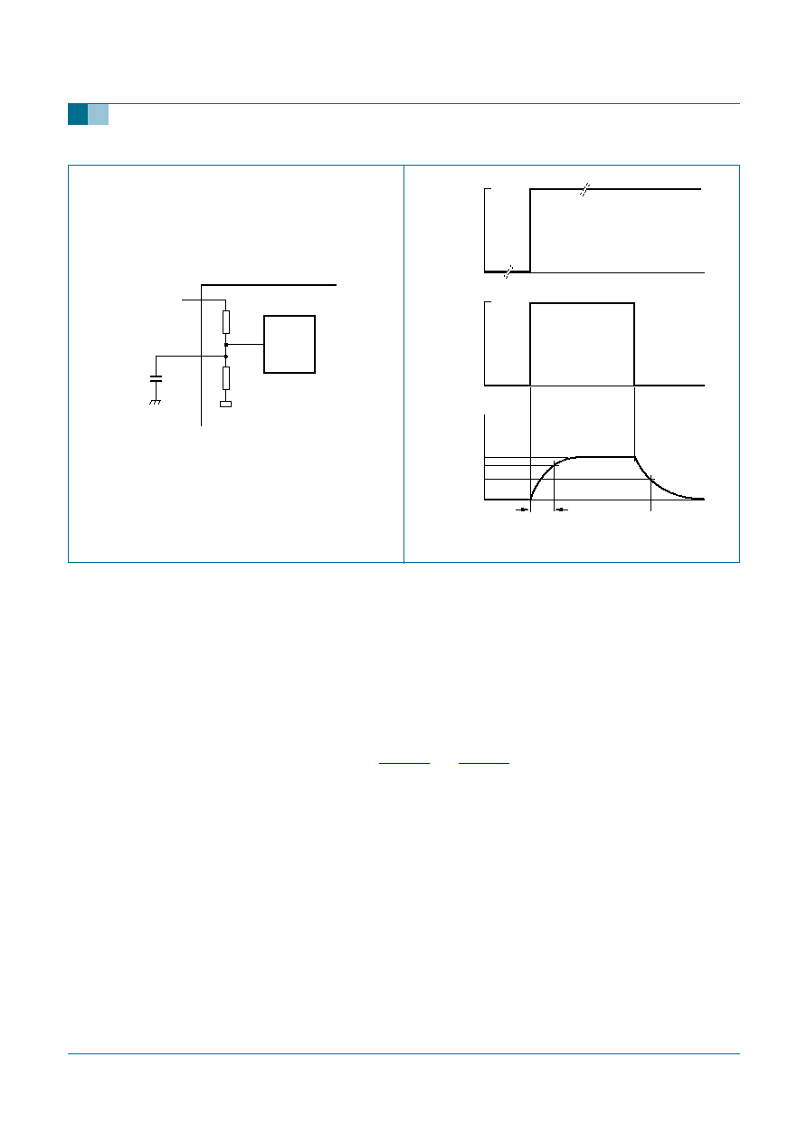
8.10 Power-on reset
The UDA1384 has an internal power-on reset circuit which initializes the device (see
Figure 5
). All the digital sound processing features and the system controlling features are
set to their default values in the L3-bus and the I
2
C-bus modes.
The reset time (see
Figure 6
) is determined by an external capacitor which is connected
between pin V
ref
and ground. The reset time should be at least 250
�
s for V
ref
< 1.25 V.
When V
DDA(AD)
is switched off, the device will be reset again for V
ref
< 0.75 V.
During the reset time, the system clock should be running.
Fig 4.
Block diagram of DAC mixer
mgw786
MIX[1:0]
DIS[1:0]
ICS[1:0]
from ADC
MIXER
VOLUME
MIXER
MUTE
DAC1
1f
s
VOLUME
DE-EMPHASIS
MUTE
DAC2
same as above
DAC3
same as above
DAC4
same as above
DAC5
same as above
DAC6
same as above
INTERPOLATION
FILTER
ch1
mixer input
ch2
ch3
ch4
from I
2
S-bus
DATADA1
DATADA2
DATADA3
+
9397 750 14366
� Koninklijke Philips Electronics N.V. 2005. All rights reserved.
Product data sheet
Rev. 02 -- 17 January 2005
11 of 55
Philips Semiconductors
UDA1384
Multichannel audio coder-decoder
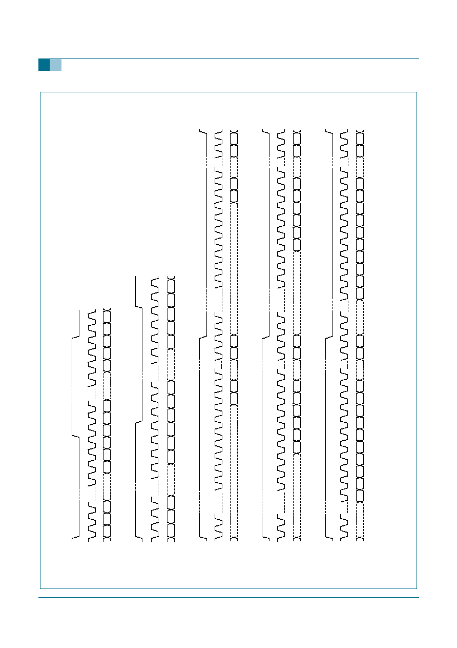
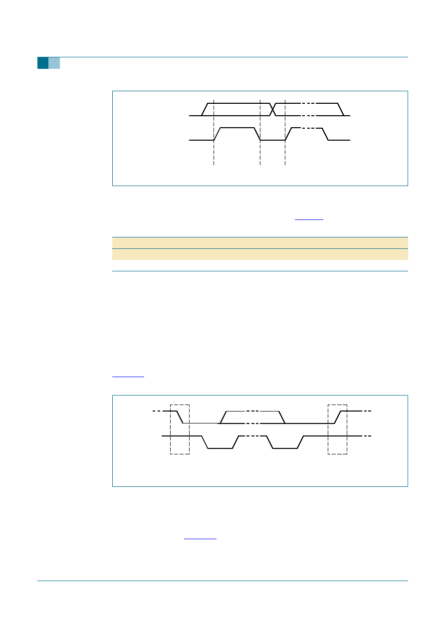
8.11 Audio digital interface
The following audio formats can be selected via the microcontroller interface:
�
I
2
S-bus format with data word length of up to 24 bits
�
MSB-justified format with data word length of up to 24 bits
�
LSB-justified format with data word length of 16 bits, 20 bits or 24 bits
�
Multichannel formats with data word length of 20 bits or 24 bits. The used data lines
are DATAAD1 and DATADA1 and the sampling frequency must be below 50 kHz
The formats are illustrated in
Figure 7
and
Figure 8
.
Fig 5.
Power-on reset circuit
Fig 6.
Power-on reset timing
V
DDA(AD)
V
ref
mgu585
C1
>
10
�
F
RESET
CIRCUIT
9 k
9 k
3.3
V
DDD
(V)
0
t
3.3
V
DDA(AD)
(V)
0
t
V
ref
(V)
1.65
1.25
0.75
t
rst
0
t
mgu586
>
250
�
s
xxxxxxxxxxxxxxxxxxxxx xxxxxxxxxxxxxxxxxxxxxxxxxx xxxxxxx x x x xxxxxxxxxxxxxxxxxxxxxxxxxxxxxx xxxxxxxxxxxxxxxxxxx xx xx
xxxxx xxxxxxxxxxxxxxxxxxxxxxxxxxx xxxxxxxxxxxxxxxxxxx xxxxxx xxxxxxxxxxxxxxxxxxxxxxxxxxxxxxxxxxx xxxxxxxxxxxx x x
xxxxxxxxxxxxxxxxxxxxx xxxxxxxxxxxxxxxxxxxxxxxxxxxxxx xxxxx xxxxxxxxxxxxxxxxxxxxxxxxxxxxxxxxxxxxxxxxxxxxxxxxxx xxxxxxxx
xxxxxxxxxxxxxxxxxxxxxxxxx xxxxxxxxxxxxxxxxxxxx xxx
9397 750 14366
� K
oninklijk
e Philips Electronics N.V
. 2005. All r
ights reser
v
ed.
Pr
oduct data sheet
Re
v
.
02 -- 17 Jan
uar
y 2005
12 of 55
Philips Semiconductor
s
UD
A1384
Multic
hannel audio coder
-decoder
Fig 7.
Formats of input and output data (single-channel)
16
MSB
B2
B3
B4
B5
B6
LEFT
LSB-JUSTIFIED FORMAT 20 BITS
WS
BCK
DATA
RIGHT
15
18
17
20
19
2
1
B19
LSB
16
MSB
B2
B3
B4
B5
B6
15
18
17
20
19
2
1
B19
LSB
MSB
MSB
B2
2
1
>
= 8
1
2
3
LEFT
I
2
S-BUS FORMAT
WS
BCK
DATA
RIGHT
3
>
= 8
MSB
B2
mgt020
16
B5
B6
B7
B8
B9
B10
LEFT
LSB-JUSTIFIED FORMAT 24 BITS
WS
BCK
DATA
RIGHT
15
18
17
20
19
22
21
23
24
2
1
B3
B4
MSB
B2
B23
LSB
16
B5
B6
B7
B8
B9
B10
15
18
17
20
19
22
21
23
24
2
1
B3
B4
MSB
B2
B23
LSB
16
MSB
B2
LEFT
LSB-JUSTIFIED FORMAT 16 BITS
WS
BCK
DATA
RIGHT
15
2
1
B15
LSB
16
MSB
B2
15
2
1
B15
LSB
MSB-JUSTIFIED FORMAT
WS
LEFT
RIGHT
3
2
1
3
2
1
MSB
B2
MSB
LSB
LSB
MSB
B2
B2
>
= 8
>
= 8
BCK
DATA
xxxxxxxxxxxxxxxxxxxxx xxxxxxxxxxxxxxxxxxxxxxxxxx xxxxxxx x x x xxxxxxxxxxxxxxxxxxxxxxxxxxxxxx xxxxxxxxxxxxxxxxxxx xx xx
xxxxx xxxxxxxxxxxxxxxxxxxxxxxxxxx xxxxxxxxxxxxxxxxxxx xxxxxx xxxxxxxxxxxxxxxxxxxxxxxxxxxxxxxxxxx xxxxxxxxxxxx x x
xxxxxxxxxxxxxxxxxxxxx xxxxxxxxxxxxxxxxxxxxxxxxxxxxxx xxxxx xxxxxxxxxxxxxxxxxxxxxxxxxxxxxxxxxxxxxxxxxxxxxxxxxx xxxxxxxx
xxxxxxxxxxxxxxxxxxxxxxxxx xxxxxxxxxxxxxxxxxxxx xxx
9397 750 14366
� K
oninklijk
e Philips Electronics N.V
. 2005. All r
ights reser
v
ed.
Pr
oduct data sheet
Re
v
.
02 -- 17 Jan
uar
y 2005
13 of 55
Philips Semiconductor
s
UD
A1384
Multic
hannel audio coder
-decoder
(1) Format 1.
(2) Format 2.
Fig 8.
Formats of input and output data (multichannel)
mgu588
MULTICHANNEL FORMAT 20 BITS
WS
BCK
DATA
2
1
22
21
CH1
42
41
61
MSB
LSB
MSB
MSB
LSB
CH3
LSB
CH5
2
1
22
21
CH2
42
41
61
MSB
LSB
MSB
MULTICHANNEL FORMAT 24 BITS
(1)
BCK
WS
WS
DATA
2
1
26
25
CH1
50
49
73
MSB
LSB
MSB
MSB
LSB
CH3
LSB
CH5
2
1
26
25
CH2
50
49
73
MSB
LSB
MSB
MSB
LSB
CH4
LSB
CH6
MULTICHANNEL FORMAT 24 BITS
(2)
BCK
DATA
1
26
25
CH1
50
49
74
MSB
LSB
MSB
73
97
CH3
MSB
LSB
CH5
LSB
1
26
25
CH2
50
49
74
MSB
LSB
MSB
73
97
CH4
MSB
LSB
CH6
LSB
MSB
LSB
CH4
LSB
CH6
9397 750 14366
� Koninklijke Philips Electronics N.V. 2005. All rights reserved.
Product data sheet
Rev. 02 -- 17 January 2005
14 of 55
Philips Semiconductors
UDA1384
Multichannel audio coder-decoder
8.12 Voice digital interface
The following voice formats can be selected via the microcontroller interface:
�
I
2
S-bus format with data word length of up to 20 bits. The left and the right channels
contain the same data.
�
Mono channel format with data word length of up to 20 bits.
The formats are illustrated in
Figure 9
.
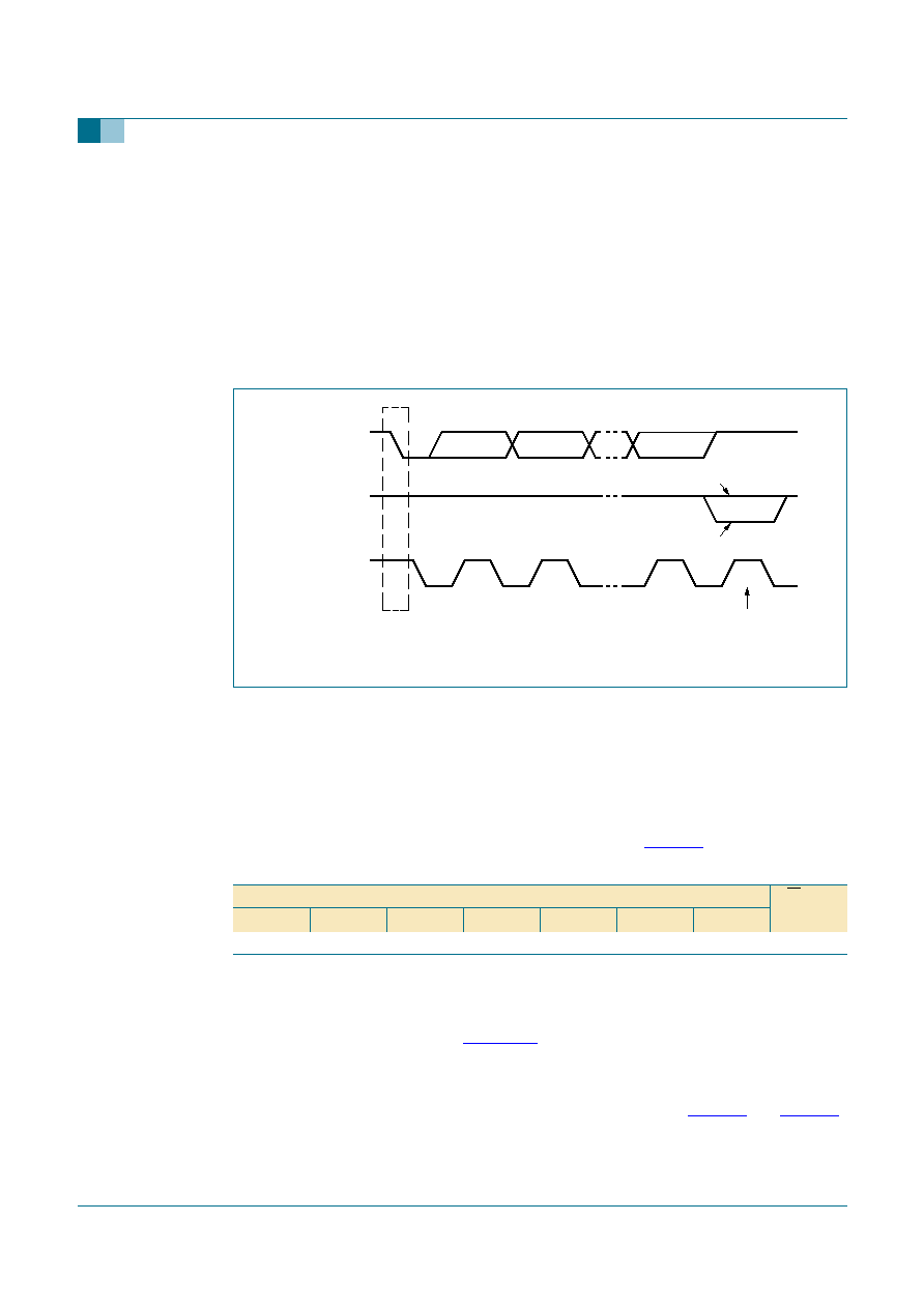
8.13 DSD mode
The UDA1384 can receive 2.8224 MHz DSD signals and generate 88.2 kHz multibit PCM
signals as well as analog signal outputs. The configuration of the UDA1384 in the DSD
mode is shown in
Figure 10
.
Fig 9.
Voice digital interface formats
mgu587
MSB
MSB
B2
2
1
8
1
2
3
LEFT
I
2
S-BUS FORMAT
WS
BCK
DATA
RIGHT
3
8
MSB
B2
MSB
B2
2
1
8
1
2
3
MONO CHANNEL FORMAT
WS
BCK
DATA
MSB
B2
Fig 10. DSD mode
mgu584
left
channel
2.8224 MHz
DSD
right
channel
5.6448 MHz
88.2 kHz
BCKAD
DATADA3
DATADA2
WSAD
WSDA
88.2 kHz
22.5792 MHz
5.6448 MHz
I
2
S-bus
(left and right)
88.2 kHz
PCM data
DATADA1
DATAAD1
BCKDA
SYSCLK
DAC
+
-
INTERPOLATION
NOISE SHAPING
I
2
S-BUS
INTERFACE 2
DECIMATION
FILTER
I
2
S-BUS
INTERFACE 1
V
OUT1N
V
OUT1P
left
channel
DAC
+
-
V
OUT2N
V
OUT2P
right
channel
analog
output

9397 750 14366
� Koninklijke Philips Electronics N.V. 2005. All rights reserved.
Product data sheet
Rev. 02 -- 17 January 2005
15 of 55
Philips Semiconductors
UDA1384
Multichannel audio coder-decoder
8.14 Microcontroller interface mode
The microcontroller interface mode can be selected as shown in
Table 11
:
�
L3-bus mode when pin I2C_L3 = LOW
�
I
2
C-bus mode when pin I2C_L3 = HIGH
All the features are accessible with the I
2
C-bus interface protocol as with the L3-bus
interface protocol.
The detailed description of the device operation in the L3-bus mode and I
2
C-bus mode is
given in
Section 9
and
Section 10
, respectively.
9.
L3-bus interface
9.1 General
The UDA1384 has an L3-bus microcontroller interface and all the digital sound processing
features and various system settings can be controlled by a microcontroller.
The exchange of data and control information between the microcontroller and the
UDA1384 is LSB first and is accomplished through a serial hardware L3-bus interface
comprising the following pins:
�
MCCLK: clock line with signal L3CLOCK
�
MCDATA: data line with signal L3DATA
�
MCMODE: mode line with signal L3MODE
The L3-bus format has two modes of operation:
�
Address mode
�
Data transfer mode
The address mode is used to select a device for a subsequent data transfer. The address
mode is characterized by signal L3MODE = LOW and a burst of 8 pulses for signal
L3CLOCK, accompanied by 8 bits (see
Figure 11
).
Table 11:
Pin function in the L3-bus or I
2
C-bus mode
Pin
Level on pin I2C_L3
LOW
HIGH
L3-bus mode signal
I
2
C-bus mode signal
MCCLK
L3CLOCK
SCL
MCDATA
L3DATA
SDA
MCMODE
L3MODE
QMUTE
Table 12:
QMUTE
Signal QMUTE
Function
LOW
no muting
HIGH
muting

9397 750 14366
� Koninklijke Philips Electronics N.V. 2005. All rights reserved.
Product data sheet
Rev. 02 -- 17 January 2005
16 of 55
Philips Semiconductors
UDA1384
Multichannel audio coder-decoder
The data transfer mode is characterized by signal L3MODE = HIGH and is used to
transfer one or more bytes representing a register address, instruction or data.
Basically, two types of data transfers can be defined:
�
Write action: data transfer to the device
�
Read action: data transfer from the device.
9.2 Device addressing
The device address consists of one byte with:
�
Data Operating Mode (DOM) bits 0 and 1 representing the type of data transfer (see
Table 13
)
�
Address bits 2 to 7 representing a 6-bit device address. The address of the UDA1384
is 01 0100 (bits 2 to 7).
9.3 Register addressing
After sending the device address (including DOM bits), indicating whether the information
is to be read or written, one data byte is sent using bit 0 to indicate whether the
information will be read or written and bits 1 to 7 for the destination register address.
Basically, there are 3 methods for register addressing:
1. Addressing for write data: bit 0 is logic 0 indicating a write action to the destination
register, followed by bits 1 to 7 indicating the register address (see
Figure 11
).
2. Addressing for prepare read: bit is logic 1, indicating that data will be read from the
register (see
Figure 12
).
3. Addressing for data read action. Here, the device returns a register address prior to
sending data from that register. When bit 0 is logic 0, the register address is valid;
when bit 0 is logic 1, the register address is invalid (see
Figure 12
).
Table 13:
Selection of data transfer
DOM
Transfer
Bit 1
Bit 0
0
0
not used
0
1
not used
1
0
write data or prepare read
1
1
read data

xxxxxxxxxxxxxxxxxxxxx xxxxxxxxxxxxxxxxxxxxxxxxxx xxxxxxx x x x xxxxxxxxxxxxxxxxxxxxxxxxxxxxxx xxxxxxxxxxxxxxxxxxx xx xx
xxxxx xxxxxxxxxxxxxxxxxxxxxxxxxxx xxxxxxxxxxxxxxxxxxx xxxxxx xxxxxxxxxxxxxxxxxxxxxxxxxxxxxxxxxxx xxxxxxxxxxxx x x
xxxxxxxxxxxxxxxxxxxxx xxxxxxxxxxxxxxxxxxxxxxxxxxxxxx xxxxx xxxxxxxxxxxxxxxxxxxxxxxxxxxxxxxxxxxxxxxxxxxxxxxxxx xxxxxxxx
xxxxxxxxxxxxxxxxxxxxxxxxx xxxxxxxxxxxxxxxxxxxx xxx
9397 750 14366
� K
oninklijk
e Philips Electronics N.V
. 2005. All r
ights reser
v
ed.
Pr
oduct data sheet
Re
v
.
02 -- 17 Jan
uar
y 2005
17 of 55
Philips Semiconductor
s
UD
A1384
Multic
hannel audio coder
-decoder
Fig 11. Data write mode
mbl567
L3CLOCK
L3MODE
L3DATA
0
write
device address
DOM bits
register address
data byte 1
data byte 2
1
0
Fig 12. Data read mode
mbl565
L3CLOCK
L3MODE
L3DATA
0
read
valid/invalid
device address
prepare read
sent by the device
DOM bits
register address
device address
requesting
register address
data byte 1
data byte 2
1
1 1
0/1
1

9397 750 14366
� Koninklijke Philips Electronics N.V. 2005. All rights reserved.
Product data sheet
Rev. 02 -- 17 January 2005
18 of 55
Philips Semiconductors
UDA1384
Multichannel audio coder-decoder
9.4 Data write mode
The data write mode is explained in the signal diagram of
Figure 11
. For writing data to a
device, 4 bytes must be sent (see
Table 14
):
1. Byte 1 starting with `01' for signalling the write action to the device, followed by the
device address `01 0100'
2. Byte 2 starting with a `0' for signalling the write action, followed by 7 bits indicating the
destination address in binary format with bit A6 being the MSB and bit A0 being the
LSB
3. Byte 3 with bit D15 being the MSB
4. Byte 4 with bit D0 being the LSB
It should be noted that each time a new destination register address needs to be written,
the device address must be sent again.
9.5 Data read mode
To read data from the device, a prepare read must first be done and then data read. The
data read mode is explained in the signal diagram of
Figure 12
.
For reading data from a device, the following 6 bytes are involved (see
Table 15
):
1. Byte 1 with the device address, including `01' for signalling the write action to the
device.
2. Byte 2 is sent with the register address from which data needs to be read. This byte
starts with a `1', which indicates that there will be a read action from the register,
followed by 7 bits for the destination address in binary format, with bit A6 being the
MSB and bit A0 being the LSB.
3. Byte 3 with the device address, including `11' is sent to the device. The `11' indicates
that the device must write data to the microcontroller.
4. Byte 4 sent by the device to the bus, with the (requested) register address and a flag
bit indicating whether the requested register was valid (bit is logic 0) or invalid (bit is
logic 1).
5. Byte 5 sent by the device to the bus, with the data information in binary format, with
bit D15 being the MSB.
6. Byte 6 sent by the device to the bus, with the data information in binary format, with
bit D0 being the LSB.
Table 14:
L3-bus write data
Byte
L3-bus
mode
Action
First in time
Latest in time
Bit 0
Bit 1
Bit 2
Bit 3
Bit 4
Bit 5
Bit 6
Bit 7
1
address
device
address
0
1
0
1
0
1
0
0
2
data
transfer
register
address
0
A6
A5
A4
A3
A2
A1
A0
3
data
transfer
data
byte 1
D15
D14
D13
D12
D11
D10
D9
D8
4
data
transfer
data
byte 2
D7
D6
D5
D4
D3
D2
D1
D0

9397 750 14366
� Koninklijke Philips Electronics N.V. 2005. All rights reserved.
Product data sheet
Rev. 02 -- 17 January 2005
19 of 55
Philips Semiconductors
UDA1384
Multichannel audio coder-decoder
10. I
2
C-bus interface
10.1 General
The UDA1384 has an I
2
C-bus microcontroller interface. All the features are accessible
with the I
2
C-bus interface protocol. In the I
2
C-bus mode, the DAC mute function is
accessible via pin MCMODE with signal QMUTE.
The exchange of data and control information between the microcontroller and the
UDA1384 is accomplished through a serial hardware interface comprising the following
pins as shown in
Table 11
:
�
MCCLK: clock line with signal SCL
�
MCDATA: data line with signal SDA
10.2 Characteristics of the I
2
C-bus
The bus is for 2-way, 2-line communication between different ICs or modules. The two
lines are a serial data line (SDA) and a serial clock line (SCL). Both lines must be
connected to the supply voltage V
DD
via a pull-up resistor when connected to the output
stages of a microcontroller. For a 400 kHz IC, the recommendation for this type of bus
from Philips Semiconductors must be followed (e.g. up to loads of 200 pF on the bus a
pull-up resistor can be used, between 200 pF and 400 pF a current source or switched
resistor must be used). Data transfer can only be initiated when the bus is not busy.
10.3 Bit transfer
One data bit is transferred during each clock pulse (see
Figure 13
). The data on the SDA
line must remain stable during the HIGH period of the clock pulse as changes in the data
line at this time will be interpreted as control signals. The maximum clock frequency is
400 kHz.
To be able to run on this high frequency, all the inputs and outputs connected to this bus
must be designed for this high-speed I
2
C-bus according to the Philips specification.
Table 15:
L3-bus read data
Byte
L3-bus
mode
Action
First in time
Latest in time
Bit 0
Bit 1
Bit 2
Bit 3
Bit 4
Bit 5
Bit 6
Bit 7
1
address
device
address
0
1
0
1
0
1
0
0
2
data
transfer
register
address
1
A6
A5
A4
A3
A2
A1
A0
3
address
device
address
1
1
0
1
0
1
0
0
4
data
transfer
register
address
0 or 1
A6
A5
A4
A3
A2
A1
A0
5
data
transfer
data
byte 1
D15
D14
D13
D12
D11
D10
D9
D8
6
data
transfer
data
byte 2
D7
D6
D5
D4
D3
D2
D1
D0
9397 750 14366
� Koninklijke Philips Electronics N.V. 2005. All rights reserved.
Product data sheet
Rev. 02 -- 17 January 2005
20 of 55
Philips Semiconductors
UDA1384
Multichannel audio coder-decoder
10.4 Byte transfer
Each byte (8 bits) is transferred with the MSB first (see
Table 16
).
10.5 Data transfer
A device generating a message is a transmitter; a device receiving a message is the
receiver. The device that controls the message is the master and the devices which are
controlled by the master are the slaves.
10.6 Start and stop conditions
Both data and clock line will remain HIGH when the bus is not busy. A HIGH-to-LOW
transition of the data line, while the clock is HIGH, is defined as a start condition (S); see
Figure 14
. A LOW-to-HIGH transition of the data line while the clock is HIGH is defined as
a stop condition (P).
10.7 Acknowledgment
The number of data bits transferred between the start and stop conditions from the
transmitter to receiver is not limited. Each byte of eight bits is followed by one
acknowledge bit (see
Figure 15
). At the acknowledge bit the data line is released by the
master and the master generates an extra acknowledge related clock pulse.
Fig 13. Bit transfer on the I
2
C-bus
mbc621
data line
stable;
data valid
change
of data
allowed
SDA
SCL
Table 16:
Byte transfer
Bit number
MSB
LSB
7
6
5
4
3
2
1
0
Fig 14. START and STOP conditions on the I
2
C-bus
mbc622
SDA
SCL
P
STOP condition
SDA
SCL
S
START condition
9397 750 14366
� Koninklijke Philips Electronics N.V. 2005. All rights reserved.
Product data sheet
Rev. 02 -- 17 January 2005
21 of 55
Philips Semiconductors
UDA1384
Multichannel audio coder-decoder
A slave receiver which is addressed, must generate an acknowledge after the reception of
each byte. Also a master must generate an acknowledge after the reception of each byte
that has been clocked out of the slave transmitter.
The device that acknowledges has to pull down the SDA line during the acknowledge
clock pulse, so the SDA line is stable LOW during the HIGH period of the acknowledge
related clock pulse. Set-up and hold times must be taken into account. A master receiver
must signal an end of data to the transmitter by not generating an acknowledge on the last
byte that has been clocked out of the slave. In this event, the transmitter must leave the
data line HIGH to enable the master to generate a stop condition.
10.8 Device address
Before any data is transmitted on the I
2
C-bus, the device which should respond is
addressed first. The addressing is always done with byte 1 transmitted after the start
procedure. The UDA1384 acts as a slave receiver or a slave transmitter.
Therefore, the clock signal SCL is only an input signal. The data signal SDA is a
bidirectional line. The UDA1384 device address is shown in
Table 17
.
10.9 Register address
The register addresses in the I
2
C-bus mode are the same as in the L3-bus mode. The
register addresses are defined in
Section 11
.
10.10 Write and read data
The I
2
C-bus configurations for a write and read cycle are shown in
Table 18
and
Table 19
,
respectively.
Fig 15. Acknowledge on the I
2
C-bus
mbc602
S
START
condition
9
8
2
1
clock pulse for
acknowledgement
not acknowledge
acknowledge
data output
by transmitter
data output
by receiver
SCL from
master
Table 17:
I
2
C-bus device address of UDA1384
Device address
R/W
A6
A5
A4
A3
A2
A1
A0
0
0
1
1
0
0
0
0/1

9397 750 14366
� Koninklijke Philips Electronics N.V. 2005. All rights reserved.
Product data sheet
Rev. 02 -- 17 January 2005
22 of 55
Philips Semiconductors
UDA1384
Multichannel audio coder-decoder
The write cycle is used to write groups of two bytes to the internal registers for the
settings. It is also possible to read the registers for the device status information.
10.11 Write cycle
The I
2
C-bus configuration for a write cycle is shown in
Table 18
. The write cycle is used to
write the data to the internal registers. The device and register addresses are one byte
each, the setting data is always a pair of two bytes.
The format of the write cycle is as follows:
1. The microcontroller starts with a start condition (S).
2. The first byte (8 bits) contains the device address `0011 000' and a logic 0 (write) for
the R/W bit.
3. This is followed by an acknowledge (A) from the UDA1384.
4. After this the microcontroller writes the 8-bit register address (ADDR) where the
writing of the register content of the UDA1384 must start.
5. The UDA1384 acknowledges this register address (A).
6. The microcontroller sends 2 bytes data with the Most Significant (MS) byte first and
then the Least Significant (LS) byte. After each byte an acknowledge is followed from
the UDA1384.
7. If repeated groups of 2 bytes data are transmitted, then the register address is auto
incremented. After each byte an acknowledge is followed from the UDA1384.
8. Finally, the UDA1384 frees the I
2
C-bus and the microcontroller can generate a stop
condition (P).
[1]
Auto increment of register address.
10.12 Read cycle
The read cycle is used to read the data values from the internal registers. The I
2
C-bus
configuration for a read cycle is shown in
Table 19
.
The format of the read cycle is as follows:
1. The microcontroller starts with a start condition (S).
2. The first byte (8 bits) contains the device address `0011 000' and a logic 0 (write) for
the R/W bit.
3. This is followed by an acknowledge (A) from the UDA1384.
4. After this the microcontroller writes the 8-bit register address (ADDR) where the
reading of the register content of the UDA1384 must start.
5. The UDA1384 acknowledges this register address.
6. Then the microcontroller generates a repeated start (Sr).
Table 18:
Master transmitter writes to UDA1384 registers in the I
2
C-bus mode
Device
address
R/W
Register
address
Data 1
Data 2
[1]
Data n
[1]
S
0011 000 0
A
ADDR
A MS1 A LS1
A MS2
A
LS2
A MSn
A LSn A
P
A = acknowledge from UDA1384
9397 750 14366
� Koninklijke Philips Electronics N.V. 2005. All rights reserved.
Product data sheet
Rev. 02 -- 17 January 2005
23 of 55
Philips Semiconductors
UDA1384
Multichannel audio coder-decoder
7. Then the microcontroller generates the device address `0011 000' again, but this time
followed by a logic 1 (read) of the R/W bit. An acknowledge is followed from the
UDA1384.
8. The UDA1384 sends 2 bytes data with the Most Significant (MS) byte first and then
the Least Significant (LS) byte. After each byte an acknowledge is followed from the
microcontroller (master).
9. If repeated groups of 2 bytes are transmitted, then the register address is auto
incremented. After each byte an acknowledge is followed from the microcontroller.
10.The microcontroller stops this cycle by generating a Negative Acknowledge (NA).
11.Finally, the UDA1384 frees the I
2
C-bus and the microcontroller can generate a stop
condition (P).
[1]
Auto increment of register address.
11. Register mapping
In this chapter the register addressing and mapping of the microcontroller interface of the
UDA1384 is given.
In
Table 20
an overview of the register mapping is given.
In
Table 21
the actual register mapping is given and the register definitions are explained
in
Section 11.3
to
Section 11.14
.
11.1 Address mapping
Table 19:
Master transmitter reads from the UDA1384 registers in the I
2
C-bus mode
Device
address
R/W
Register
address
Device
address
R/W Data 1
Data 2
[1]
Data n
[1]
S
0011 000 0
A
ADDR
A
Sr 0011 000 1 A
MS1 A
LS1
A
MS2 A
LS2
A
MSn A
LSn
NA
P
A = acknowledge from UDA1384
A = acknowledge from master
Table 20:
Overview of register mapping
Address
Function
System settings
00h
system
01h
audio ADC and DAC subsystem
02h
voice ADC system
Status (read out registers)
0Fh
status outputs
Interpolator settings
10h
DAC channel and feature selection
11h
DAC feature control
12h
DAC channel 1
13h
DAC channel 2
14h
DAC channel 3
15h
DAC channel 4

9397 750 14366
� Koninklijke Philips Electronics N.V. 2005. All rights reserved.
Product data sheet
Rev. 02 -- 17 January 2005
24 of 55
Philips Semiconductors
UDA1384
Multichannel audio coder-decoder
16h
DAC channel 5
17h
DAC channel 6
18h
DAC mixing channel 1
19h
DAC mixing channel 2
1Ah
DAC mixing channel 3
1Bh
DAC mixing channel 4
1Ch
DAC mixing channel 5
1Dh
DAC mixing channel 6
ADC input amplifier gain settings
20h
audio ADC input amplifier gain
21h
voice ADC input amplifier gain
Supplemental settings
30h
supplemental settings 1
31h
supplemental settings 2
Table 20:
Overview of register mapping
...continued
Address
Function

xxxxxxxxxxxxxxxxxxxxx xxxxxxxxxxxxxxxxxxxxxxxxxx xxxxxxx x x x xxxxxxxxxxxxxxxxxxxxxxxxxxxxxx xxxxxxxxxxxxxxxxxxx xx xx
xxxxx xxxxxxxxxxxxxxxxxxxxxxxxxxx xxxxxxxxxxxxxxxxxxx xxxxxx xxxxxxxxxxxxxxxxxxxxxxxxxxxxxxxxxxx xxxxxxxxxxxx x x
xxxxxxxxxxxxxxxxxxxxx xxxxxxxxxxxxxxxxxxxxxxxxxxxxxx xxxxx xxxxxxxxxxxxxxxxxxxxxxxxxxxxxxxxxxxxxxxxxxxxxxxxxx xxxxxxxx
xxxxxxxxxxxxxxxxxxxxxxxxx xxxxxxxxxxxxxxxxxxxx xxx
9397 750 14366
� K
oninklijk
e Philips Electronics N.V
. 2005. All r
ights reser
v
ed.
Pr
oduct data sheet
Re
v
.
02 -- 17 Jan
uar
y 2005
25 of 55
Philips Semiconductor
s
UD
A1384
Multic
hannel audio coder
-decoder
11.2 Register mapping
Table 21:
UDA1384 register mapping
[1]
Add
Function
D15
D14
D13
D12
D11
D10
D9
D8
D7
D6
D5
D4
D3
D2
D1
D0
System settings
00h
system
RST
[2]
VFS1
VFS0
VCE
VAP
DSD
SC1
SC0
OP1
OP0
FS1
FS0
ACE
ADP
DCE
DAP
-
0
0
1
0
0
0
0
0
0
0
1
1
0
1
0
01h
audio ADC and DAC
subsystem
DC
PAB
PAA
MTB
MTA
AIF2
AIF1
AIF0
DAG
FIL
DVD
DIS1
DIS0
DIF2
DIF1
DIF0
1
0
0
0
0
0
0
0
0
0
0
0
0
0
0
0
02h
voice ADC system
-
-
-
-
-
-
-
-
BCK1
BCK0
WSM
VH1
VH0
PVA
MTV
VIF
0
0
0
0
0
0
0
0
0
1
1
0
1
0
0
0
Status (read out only)
0Fh
status outputs
-
-
-
-
-
-
-
-
-
-
VS
AS1
AS0
DS2
DS1
DS0
Interpolator settings
10h
DAC channel and
feature selection
MIX1
MIX0
MC5
MC4
MC3
MC2
MC1
MC0
SEL1
SEL0
CS5
CS4
CS3
CS2
CS1
CS0
0
0
0
0
0
0
0
0
0
0
0
0
0
0
0
0
11h
DAC feature control
ICS1
ICS0
DE2
DE1
DE0
PD
MT
QM
VC7
VC6
VC5
VC4
VC3
VC2
VC1
VC0
0
0
0
0
0
0
0
0
0
0
0
0
0
0
0
0
12h
DAC channel 1
ICS1
ICS0
DE2
DE1
DE0
PD
MT
QM
VC7
VC6
VC5
VC4
VC3
VC2
VC1
VC0
0
0
0
0
0
0
0
0
0
0
0
0
0
0
0
0
13h
DAC channel 2
-
-
DE2
DE1
DE0
PD
MT
QM
VC7
VC6
VC5
VC4
VC3
VC2
VC1
VC0
0
0
0
0
0
0
0
0
0
0
0
0
0
0
0
0
14h
DAC channel 3
ICS1
ICS0
DE2
DE1
DE0
PD
MT
QM
VC7
VC6
VC5
VC4
VC3
VC2
VC1
VC0
0
0
0
0
0
0
0
0
0
0
0
0
0
0
0
0
15h
DAC channel 4
-
-
DE2
DE1
DE0
PD
MT
QM
VC7
VC6
VC5
VC4
VC3
VC2
VC1
VC0
0
0
0
0
0
0
0
0
0
0
0
0
0
0
0
0
16h
DAC channel 5
ICS1
ICS0
DE2
DE1
DE0
PD
MT
QM
VC7
VC6
VC5
VC4
VC3
VC2
VC1
VC0
0
0
0
0
0
0
0
0
0
0
0
0
0
0
0
0
17h
DAC channel 6
-
-
DE2
DE1
DE0
PD
MT
QM
VC7
VC6
VC5
VC4
VC3
VC2
VC1
VC0
0
0
0
0
0
0
0
0
0
0
0
0
0
0
0
0
18h
DAC mixing
channel 1
ICS1
ICS0
-
-
-
PD
MT
QM
VC7
VC6
VC5
VC4
VC3
VC2
VC1
VC0
0
0
0
0
0
0
0
0
0
0
0
0
0
0
0
0

xxxxxxxxxxxxxxxxxxxxx xxxxxxxxxxxxxxxxxxxxxxxxxx xxxxxxx x x x xxxxxxxxxxxxxxxxxxxxxxxxxxxxxx xxxxxxxxxxxxxxxxxxx xx xx
xxxxx xxxxxxxxxxxxxxxxxxxxxxxxxxx xxxxxxxxxxxxxxxxxxx xxxxxx xxxxxxxxxxxxxxxxxxxxxxxxxxxxxxxxxxx xxxxxxxxxxxx x x
xxxxxxxxxxxxxxxxxxxxx xxxxxxxxxxxxxxxxxxxxxxxxxxxxxx xxxxx xxxxxxxxxxxxxxxxxxxxxxxxxxxxxxxxxxxxxxxxxxxxxxxxxx xxxxxxxx
xxxxxxxxxxxxxxxxxxxxxxxxx xxxxxxxxxxxxxxxxxxxx xxx
9397 750 14366
� K
oninklijk
e Philips Electronics N.V
. 2005. All r
ights reser
v
ed.
Pr
oduct data sheet
Re
v
.
02 -- 17 Jan
uar
y 2005
26 of 55
Philips Semiconductor
s
UD
A1384
Multic
hannel audio coder
-decoder
[1]
When writing new settings via the L3-bus interface, the default values should always be set to warrant correct operation. Read access to the DAC features register 11h will not
return valid data.
[2]
When bit RST is set to logic 1, the default values are set to all the registers as shown in
Table 21
. When start-up, all the registers in 00h are initialized as the default values and the
mute control bits MTA, MTB, MTV, MT and QM are set to logic 1. All other registers have non fixed values.
19h
DAC mixing
channel 2
-
-
-
-
-
PD
MT
QM
VC7
VC6
VC5
VC4
VC3
VC2
VC1
VC0
0
0
0
0
0
0
0
0
0
0
0
0
0
0
0
0
1Ah
DAC mixing
channel 3
ICS1
ICS0
-
-
-
PD
MT
QM
VC7
VC6
VC5
VC4
VC3
VC2
VC1
VC0
0
0
0
0
0
0
0
0
0
0
0
0
0
0
0
0
1Bh
DAC mixing
channel 4
-
-
-
-
-
PD
MT
QM
VC7
VC6
VC5
VC4
VC3
VC2
VC1
VC0
0
0
0
0
0
0
0
0
0
0
0
0
0
0
0
0
1Ch
DAC mixing
channel 5
ICS1
ICS0
-
-
-
PD
MT
QM
VC7
VC6
VC5
VC4
VC3
VC2
VC1
VC0
0
0
0
0
0
0
0
0
0
0
0
0
0
0
0
0
1Dh
DAC mixing
channel 6
-
-
-
-
-
PD
MT
QM
VC7
VC6
VC5
VC4
VC3
VC2
VC1
VC0
0
0
0
0
0
0
0
0
0
0
0
0
0
0
0
0
ADC input amplifier gain settings
20h
ADC 1 and ADC 2
input amplifier gain
-
-
-
-
IB3
IB2
IB1
IB0
-
-
-
-
IA3
IA2
IA1
IA0
0
0
0
0
0
0
0
0
0
0
0
0
0
0
0
0
21h
voice ADC input
amplifier gain
-
-
-
-
-
-
-
-
-
-
-
IV4
IV3
IV2
IV1
IV0
-
-
-
-
-
-
-
-
0
0
0
0
0
0
0
0
Supplemental settings
30h
supplemental
settings 1
-
-
-
-
-
-
-
-
PDT
-
-
-
-
-
-
-
0
0
0
0
0
0
0
0
0
0
0
0
0
0
0
0
31h
supplemental
settings 2
-
-
-
-
-
-
-
-
-
DITH2 DITH1 DITH0 -
-
VMTP PDLNA
0
0
0
0
0
0
0
0
0
0
0
0
0
0
0
0
Table 21:
UDA1384 register mapping
[1]
...continued
Add
Function
D15
D14
D13
D12
D11
D10
D9
D8
D7
D6
D5
D4
D3
D2
D1
D0

9397 750 14366
� Koninklijke Philips Electronics N.V. 2005. All rights reserved.
Product data sheet
Rev. 02 -- 17 January 2005
27 of 55
Philips Semiconductors
UDA1384
Multichannel audio coder-decoder
11.3 System settings
Table 22:
System register (address 00h) bit allocation
Bit
15
14
13
12
11
10
9
8
Symbol
RST
VFS1
VFS0
VCE
VAP
DSD
SC1
SC0
Reset
-
0
0
1
0
0
0
0
Access
read and write
Bit
7
6
5
4
3
2
1
0
Symbol
OP1
OP0
FS1
FS0
ACE
ADP
DCE
DAP
Reset
0
0
0
1
1
0
1
0
Access
read and write
Table 23:
Description of system register bits
Bit
Symbol
Description
15
RST
Reset. Bit RST initializes the L3-bus registers with the default settings.
1 = Reset to default settings
0 = No reset
14 to 13
VFS[1:0]
Voice ADC sampling frequency. A 2-bit value to select the voice ADC
sampling frequency. Default 00. See
Table 24
.
12
VCE
Voice ADC clock enable.
1 = clock enabled (default)
0 = clock disabled
11
VAP
Voice ADC power control. Bit VAP is to reduce the power consumption of
the voice ADC.
1 = state is power-on
0 = state is power-off (default)
10
DSD
DSD mode selection. Bit DSD selects the DSD mode.
1 = DSD mode
0 = normal mode (default)
9 to 8
SC[1:0]
System clock frequency. A 2-bit value to select the used external clock
frequency. 128f
s
system clock for the DAC can be used by setting
bit DVD = 1. Default 00. See
Table 25
.
7 to 6
OP[1:0]
Operating mode selection. A 2-bit value to select the operation mode of
the audio ADC and DAC. Default 00. See
Table 26
.
5 to 4
FS[1:0]
Sampling frequency. A 2-bit value to select the sampling frequency of the
audio ADC and DAC in the WS mode. Default 01. See
Table 27
.
3
ACE
ADC clock enable. Bit ACE enables the audio ADC clock
1 = clock enabled (default)
0 = clock disabled
2
ADP
ADC power control. Bit ADP is to reduce the power consumption of the
audio ADC.
1 = state is power-on
0 = state is power-off (default)

9397 750 14366
� Koninklijke Philips Electronics N.V. 2005. All rights reserved.
Product data sheet
Rev. 02 -- 17 January 2005
28 of 55
Philips Semiconductors
UDA1384
Multichannel audio coder-decoder
1
DCE
DAC clock enable. Bit DCE enables the DAC clock.
1 = clock enabled (default)
0 = clock disabled
0
DAP
DAC power control. Bit DAP is to reduce the power consumption of the
DAC.
1 = state is power-on
0 = state is power-off (default)
Table 24:
Voice ADC sampling frequency bits
VFS1
VFS0
Function
0
0
6.25 kHz to 12.5 kHz (default)
0
1
12.5 kHz to 25 kHz
1
0
25 kHz to 50 kHz
1
1
reserved
Table 25:
System clock frequency bits
SC1
SC0
ADC
DAC
Remark
Bit DVD = 0
Bit DVD = 1
0
0
256f
s
256f
s
128f
s
default
0
1
384f
s
384f
s
192f
s
1
0
512f
s
512f
s
256f
s
1
1
768f
s
768f
s
384f
s
Table 26:
Operating mode bits
OP1
OP0
ADC mode
DAC mode
Remark
0
0
SYSCLK (256f
s
, 384f
s
, 512f
s
or 768f
s
)
SYSCLK (128f
s
, 256f
s
, 384f
s
,
512f
s
or 768f
s
)
default
0
1
SYSCLK (256f
s
, 384f
s
, 512f
s
or 768f
s
)
WSDA (1f
s
)
1
0
WSAD (1f
s
)
SYSCLK (128f
s
, 256f
s
, 384f
s
,
512f
s
or 768f
s
)
1
1
WSDA (1f
s
)
WSDA (1f
s
)
Table 27:
Audio ADC and DAC sampling frequency bits
FS1
FS0
Function
0
0
12.5 kHz to 25 kHz
0
1
25 kHz to 50 kHz (default)
1
0
50 kHz to 100 kHz
1
1
100 kHz to 200 kHz
Table 23:
Description of system register bits
...continued
Bit
Symbol
Description

9397 750 14366
� Koninklijke Philips Electronics N.V. 2005. All rights reserved.
Product data sheet
Rev. 02 -- 17 January 2005
29 of 55
Philips Semiconductors
UDA1384
Multichannel audio coder-decoder
11.4 Audio ADC and DAC subsystem settings
Table 28:
Audio ADC and DAC subsystem register (address 01h) bit allocation
Bit
15
14
13
12
11
10
9
8
Symbol
DC
PAB
PAA
MTB
MTA
AIF2
AIF1
AIF0
Reset
1
0
0
0
0
0
0
0
Access
read and write
Bit
7
6
5
4
3
2
1
0
Symbol
DAG
FIL
DVD
DIS1
DIS0
DIF2
DIF1
DIF0
Reset
0
0
0
0
0
0
0
0
Access
read and write
Table 29:
Description of the audio ADC and DAC subsystem register bit
Bit
Symbol
Description
15
DC
ADC DC-filter. Bit DC enables the digital DC-filter of the ADC.
1 = DC-filtering is active (default)
0 = no DC-filtering
14
PAB
Polarity ADC 2 control. Bit PAB controls the ADC 2 polarity.
1 = polarity is inverted
0 = polarity is not-inverted (default)
13
PAA
Polarity ADC 1 control. Bit PAA controls the ADC 1 polarity.
1 = polarity is inverted
0 = polarity is not-inverted (default)
12
MTB
Mute ADC 2. Bit MTB enables the digital mute of ADC 2.
1 = ADC 2 is soft muted
0 = ADC 2 is not muted (default)
11
MTA
Mute ADC 1. Bit MTA enables the digital mute of ADC 1.
1 = ADC 1 is soft muted
0 = ADC 1 is not muted (default)
10 to 8
AIF[2:0]
ADC output data interface format. A 3-bit value to select the used data
format to the I
2
S-bus ADC output interface. Default 000. See
Table 30
.
7
DAG
DAC gain switch. Bit DAG selects the DAC gain.
1 = gain = 6 dB
0 = gain = 0 dB (default)
6
FIL
Filter selection. Bit FIL selects the interpolation filter characteristics.
1 = slow roll-off
0 = sharp roll-off (default)
5
DVD
192 kHz sampling mode selection. Bit DVD selects the oversampling rate
of the noise shaper.
1 = 64f
s
rate; used for 192 kHz and 176.4 kHz sampling frequencies
0 = 128f
s
rate (default)
4 to 3
DIS[1:0]
Data interface selection. A 2-bit value to select the data interface
connection. Default 00. See
Table 31
.
2 to 0
DIF[2:0]
DAC input data interface format. A 3-bit value to select the used data
format to the I
2
S-bus DAC input interface. Default 000. See
Table 30
.

9397 750 14366
� Koninklijke Philips Electronics N.V. 2005. All rights reserved.
Product data sheet
Rev. 02 -- 17 January 2005
30 of 55
Philips Semiconductors
UDA1384
Multichannel audio coder-decoder
11.5 Voice ADC system settings
Table 30:
Data interface format bits
AIF2
AIF1
AIF0
Function
DIF2
DIF1
DIF0
0
0
0
I
2
S-bus format (default)
0
0
1
LSB-justified format, 16 bits
0
1
0
LSB-justified format, 20 bits
0
1
1
LSB-justified format, 24 bits
1
0
0
MSB-justified format
1
0
1
multichannel format, 20 bits
1
1
0
multichannel format, 24 bits (format 1)
1
1
1
multichannel format, 24 bits (format 2)
Table 31:
Data interface selection bits
DIS1
DIS0
Input to DAC
0
0
DATADA1 to DAC channel 1 and 2, DATADA2 to DAC channel 3
and 4, and DATADA3 to DAC channel 5 and 6 (default)
0
1
DATADA1 to DAC channels 1 to 6
1
0
DATADA2 to DAC channels 1 to 6
1
1
DATADA3 to DAC channels 1 to 6
Table 32:
Voice ADC system register (address 02h) bit allocation
Bit
15
14
13
12
11
10
9
8
Symbol
-
-
-
-
-
-
-
-
Reset
-
-
-
-
-
-
-
-
Access
read and write
Bit
7
6
5
4
3
2
1
0
Symbol
BCK1
BCK0
WSM
VH1
VH0
PVA
MTV
VIF
Reset
0
1
1
0
1
0
0
0
Access
read and write
Table 33:
Description of the voice ADC system register bits
Bit
Symbol
Description
15 to 8
-
default 0000 0000
7 to 6
BCK[1:0]
BCK frequency of voice ADC. A 2-bit value to select the BCK
frequency of the voice ADC in the WSV-out mode. Default 01.
See
Table 34
.
5
WSM
WSV mode selection. Bit WSM selects the WSV mode of the voice
ADC
1 = WSV-in mode (default)
0 = WSV-out mode
4 to 3
VH[1:0]
Voice ADC high-pass filter setting. A 2-bit value to enable the
high-pass filter of the voice ADC. Default 01. See
Table 35
.

9397 750 14366
� Koninklijke Philips Electronics N.V. 2005. All rights reserved.
Product data sheet
Rev. 02 -- 17 January 2005
31 of 55
Philips Semiconductors
UDA1384
Multichannel audio coder-decoder
2
PVA
Polarity voice ADC control. Bit PVA controls the voice ADC polarity.
1 = polarity is inverted
0 = polarity is not-inverted (default)
1
MTV
Mute voice ADC. Bit MTV enables the digital mute of the voice ADC.
1 = ADC 1 is soft muted
0 = ADC 1 is not muted (default)
0
VIF
Voice ADC interface format. Bit VIF selects the data interface format
of the voice ADC.
1 = mono-channel format
0 = I
2
S-bus format (default)
Table 34:
BCK frequency of voice ADC bits
BCK1
BCK0
Function
0
0
32f
s
0
1
64f
s
(default)
1
0
128f
s
1
1
256f
s
Table 35:
Voice ADC high-pass filter setting bits
VH1
VH0
Function
0
0
high-pass filter off
0
1
f
c
= 0.00008f
s
(default)
1
0
f
c
= 0.0125f
s
1
1
f
c
= 0.025f
s
Table 33:
Description of the voice ADC system register bits
...continued
Bit
Symbol
Description

9397 750 14366
� Koninklijke Philips Electronics N.V. 2005. All rights reserved.
Product data sheet
Rev. 02 -- 17 January 2005
32 of 55
Philips Semiconductors
UDA1384
Multichannel audio coder-decoder
11.6 Status output register
Table 36:
Status output register (address 0Fh) bit allocation
Bit
15
14
13
12
11
10
9
8
Symbol
-
-
-
-
-
-
-
-
Reset
-
-
-
-
-
-
-
-
Access
read only
Bit
7
6
5
4
3
2
1
0
Symbol
-
-
VS
AS1
AS0
DS2
DS1
DS0
Reset
-
-
-
-
-
-
-
-
Access
read only
Table 37:
Description of status output register bits
Bit
Symbol
Description
15 to 6
-
not used
5
VS
Voice ADC status. Bit VS indicates the hard mute status of the voice ADC.
1 = power-down is ready and the clock may be disabled
0 = power-down is not ready and the clock should not be disabled
4
AS1
ADC 2 status. Bit AS1 indicates the hard mute status of ADC 2.
1 = power-down is ready and the clock may be disabled
0 = power-down is not ready and the clock should not be disabled
3
AS0
ADC 1 status. Bit AS0 indicates the hard mute status of ADC 1.
1 = power-down is ready and the clock may be disabled
0 = power-down is not ready and the clock should not be disabled
2
DS2
DAC channel 5 and 6 status. Bit DS2 indicates the hard mute status of DAC
channel 5 and 6.
1 = power-down is ready and the clock may be disabled
0 = power-down is not ready and the clock should not be disabled
1
DS1
DAC channel 3 and 4 status. Bit DS1 indicates the hard mute status of DAC
channel 3 and 4.
1 = power-down is ready and the clock may be disabled
0 = power-down is not ready and the clock should not be disabled
0
DS0
DAC channel 1 and 2 status. Bit DS0 indicates the hard mute status of DAC
channel 1 and 2.
1 = power-down is ready and the clock may be disabled
0 = power-down is not ready and the clock should not be disabled

9397 750 14366
� Koninklijke Philips Electronics N.V. 2005. All rights reserved.
Product data sheet
Rev. 02 -- 17 January 2005
33 of 55
Philips Semiconductors
UDA1384
Multichannel audio coder-decoder
11.7 DAC channel selection
Table 38:
DAC channel select register (address 10h) bit allocation
Bit
15
14
13
12
11
10
9
8
Symbol
MIX1
MIX0
MC5
MC4
MC3
MC2
MC1
MC0
Reset
0
0
0
0
0
0
0
0
Access
read and write
Bit
7
6
5
4
3
2
1
0
Symbol
SEL1
SEL0
CS5
CS4
CS3
CS2
CS1
CS0
Reset
0
0
0
0
0
0
0
0
Access
read and write
Table 39:
Description of DAC channel select register bits
Bit
Symbol
Description
15 to 14
MIX[1:0]
DAC mixer setting. A 2-bit value to enable the DAC mixer. Default 00.
See
Table 40
.
13 to 8
MC[5:0]
DAC mixing channel selection. A group of 6 enable bits to make DAC
mixing channels ready for receiving feature settings through register
address 11h. Only selected registers accept new settings. Default 00 0000
(no channel ready). See
Table 41
.
7 and 6
SEL[1:0]
Feature selection. A 2-bit value to select the features to be set through
register address 11h. When the feature settings are written, only selected
feature settings are changed and non selected features are kept
unchanged. Default 00. See
Table 42
.
5 to 0
CS[5:0]
DAC channel selection. A group of 6 enable bits to make DAC channel
ready for receiving feature settings through register address 11h.
Default 00 0000 (no channel ready). See
Table 41
.
Table 40:
DAC mixer setting bits
MIX1
MIX0
Function
0
0
no mixing (default)
0
1
no mixing
1
0
mixing ADC 1
1
1
mixing ADC 2
Table 41:
DAC channel and mixing channel selection bits
MC5
MC4
MC3
MC2
MC1
MC0
Function
CS5
CS4
CS3
CS2
CS1
CS0
0
0
0
0
0
0
no channel ready (default)
0
0
0
0
0
1
channel 1 selected
:
:
:
:
:
:
0
0
1
0
1
0
channel 2 and channel 4 selected
:
:
:
:
:
:
1
1
1
1
1
1
all channels selected

9397 750 14366
� Koninklijke Philips Electronics N.V. 2005. All rights reserved.
Product data sheet
Rev. 02 -- 17 January 2005
34 of 55
Philips Semiconductors
UDA1384
Multichannel audio coder-decoder
11.8 DAC features settings
Table 42:
Feature selection bits
SEL1
SEL0
Function
0
0
all features (default)
0
1
volume
1
0
mute and quick mute
1
1
de-emphasis, polarity and input channel selection
Table 43:
DAC features register (address 11h) bit allocation
Bit
15
14
13
12
11
10
9
8
Symbol
ICS1
ICS0
DE2
DE1
DE0
PD
MT
QM
Reset
0
0
0
0
0
0
0
0
Access
read and write
Bit
7
6
5
4
3
2
1
0
Symbol
VC7
VC6
VC5
VC4
VC3
VC2
VC1
VC0
Reset
0
0
0
0
0
0
0
0
Access
read and write
Table 44:
Description of DAC features register bits
Bit
Symbol
Description
15 to 14
ICS[1:0]
Input channel selection. A 2-bit value to select the input channels. As
the controlled channels are paired off, this 2-bit value must be written
to each odd channel register. Default 00. See
Table 45
.
13 to 11
DE[2:0]
De-emphasis setting. A 3-bit value to enable the digital de-emphasis
filter. Default 000. See
Table 46
.
10
PD
Polarity DAC control. Bit PD controls the DAC polarity.
1 = polarity is inverted
0 = polarity is not-inverted (default)
9
MT
Muting. Bit MT enables the digital mute. All the DAC outputs are
muted at start-up. It is necessary to explicitly switch off for the audio
output by means of bit MT.
1 = muting (start-up)
0 = no muting (default)
8
QM
Quick mute. Bit QM sets the quick mute mode.
1 = quick mute mode
0 = soft mute mode (default)
7 to 0
VC[7:0]
Interpolator volume control. An 8-bit value to program the volume
attenuation of each channel. The range is from 0 dB to
-
53 dB in steps
of 0.25 dB, from
-
53 dB to
-
80 dB in steps of 3 dB and
-
dB.
Default 0000 0000. See
Table 47
.

9397 750 14366
� Koninklijke Philips Electronics N.V. 2005. All rights reserved.
Product data sheet
Rev. 02 -- 17 January 2005
35 of 55
Philips Semiconductors
UDA1384
Multichannel audio coder-decoder
Table 45:
Input channel selection bits
ICS1
ICS0
Input to DAC output
0
0
left channel input data to odd channel output; right channel input
data to even channel output
0
1
left channel input data to odd and even channel outputs
1
0
right channel input data to odd and even channel outputs
1
1
left channel input data to even channel output; right channel input
data to odd channel output
Table 46:
De-emphasis bits
DE2
DE1
DE0
Function
0
0
0
no de-emphasis (default)
0
0
1
de-emphasis of 32 kHz
0
1
0
de-emphasis of 44.1 kHz
0
1
1
de-emphasis of 48 kHz
1
0
0
de-emphasis of 96 kHz
1
0
1
not used
1
1
0
not used
1
1
1
not used
Table 47:
Interpolator volume control bits
VC7
VC6
VC5
VC4
VC3
VC2
VC1
VC0
Volume (dB)
0
0
0
0
0
0
0
0
0 (default)
0
0
0
0
0
0
0
1
-
0.25
0
0
0
0
0
0
1
0
-
0.50
0
0
0
0
0
0
1
1
-
0.75
0
0
0
0
0
1
0
0
-
1.00
0
0
0
0
0
1
0
1
-
1.25
:
:
:
:
:
:
:
:
:
1
1
0
1
0
1
0
0
-
53
1
1
0
1
1
0
0
0
-
56
1
1
0
1
1
1
0
0
-
59
1
1
1
0
0
0
0
0
-
62
1
1
1
0
0
1
0
0
-
65
1
1
1
0
1
0
0
0
-
68
1
1
1
0
1
1
0
0
-
71
1
1
1
1
0
0
0
0
-
74
1
1
1
1
0
1
0
0
-
77
1
1
1
1
1
0
0
0
-
80
1
1
1
1
1
1
0
0
-
:
:
:
:
:
:
:
:
:
1
1
1
1
1
1
1
1
-
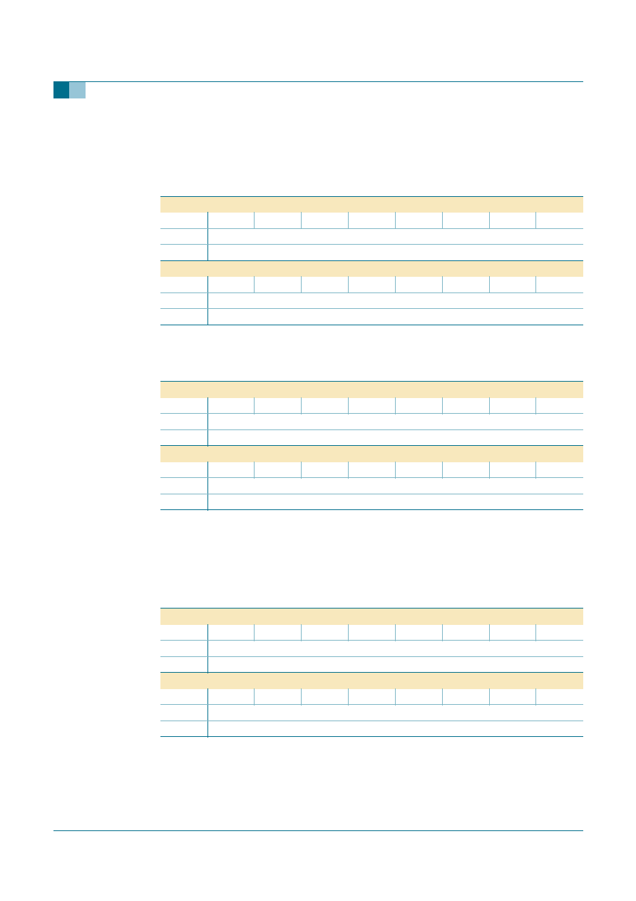
9397 750 14366
� Koninklijke Philips Electronics N.V. 2005. All rights reserved.
Product data sheet
Rev. 02 -- 17 January 2005
36 of 55
Philips Semiconductors
UDA1384
Multichannel audio coder-decoder
11.9 DAC channel 1 to channel 6 settings
All the DAC features which are written in register 11h are copied into the odd channel
registers.
All the DAC features which are written in register 11h are copied into the even channel
registers, except the bits ICS[1:0].
11.10 DAC mixing channel settings
All the DAC features which are written in register 11h are copied into the odd mixing
channel registers, except the bits DE[2:0].
Table 48:
DAC channel 1, 3 and 5 registers (address 12h, 14h and 16h) bit allocation
Bit
15
14
13
12
11
10
9
8
Symbol
ICS1
ICS0
DE2
DE1
DE0
PD
MT
QM
Reset
0
0
0
0
0
0
0
0
Access
read and write
Bit
7
6
5
4
3
2
1
0
Symbol
VC7
VC6
VC5
VC4
VC3
VC2
VC1
VC0
Reset
0
0
0
0
0
0
0
0
Access
read and write
Table 49:
DAC channel 2, 4 and 6 registers (address 13h, 15h and 17h) bit allocation
Bit
15
14
13
12
11
10
9
8
Symbol
-
-
DE2
DE1
DE0
PD
MT
QM
Reset
0
0
0
0
0
0
0
0
Access
read and write
Bit
7
6
5
4
3
2
1
0
Symbol
VC7
VC6
VC5
VC4
VC3
VC2
VC1
VC0
Reset
0
0
0
0
0
0
0
0
Access
read and write
Table 50:
DAC mixing channel 1, 3 and 5 registers (address 18h, 1Ah and 1Ch) bit
allocation
Bit
15
14
13
12
11
10
9
8
Symbol
ICS1
ICS0
-
-
-
PD
MT
QM
Reset
0
0
0
0
0
0
0
0
Access
read and write
Bit
7
6
5
4
3
2
1
0
Symbol
VC7
VC6
VC5
VC4
VC3
VC2
VC1
VC0
Reset
0
0
0
0
0
0
0
0
Access
read and write
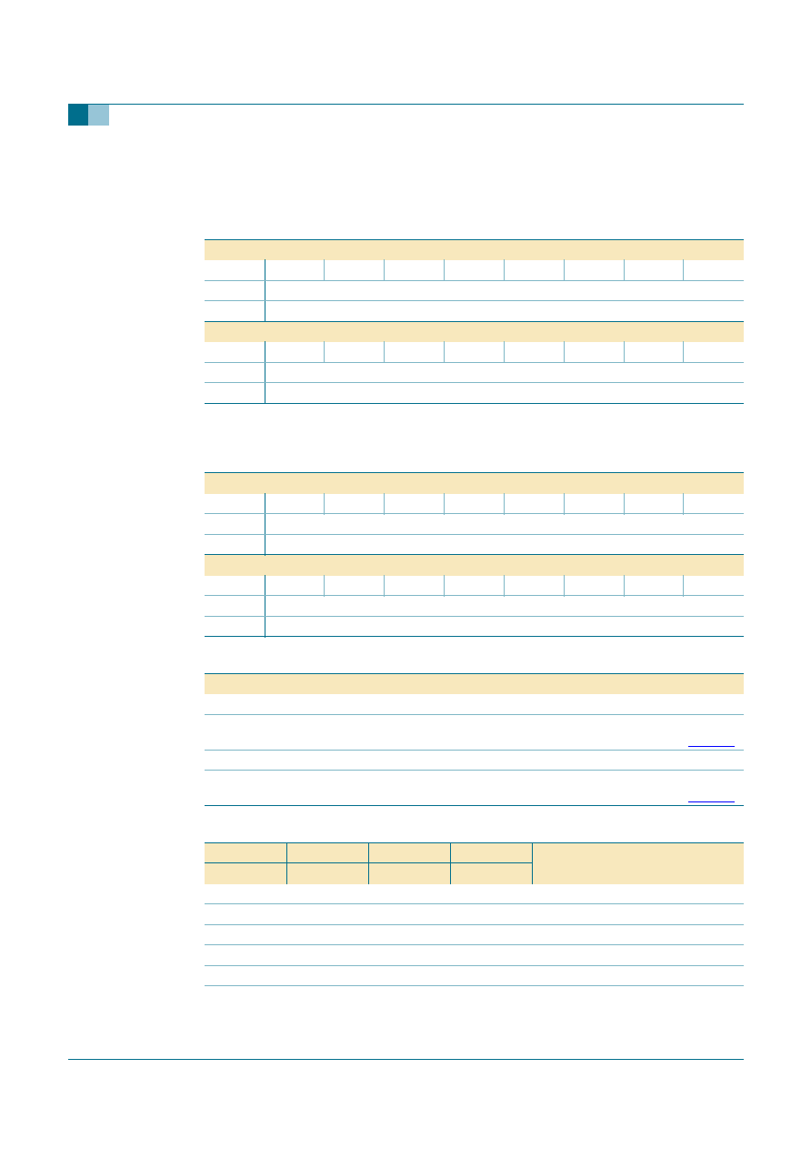
9397 750 14366
� Koninklijke Philips Electronics N.V. 2005. All rights reserved.
Product data sheet
Rev. 02 -- 17 January 2005
37 of 55
Philips Semiconductors
UDA1384
Multichannel audio coder-decoder
All the DAC features which are written in register 11h are copied into the even channel
registers, except the bits ICS[1:0] and DE[2:0].
11.11 Audio ADC 1 and ADC 2 input amplifier gain settings
Table 51:
DAC mixing channel 2, 4 and 6 registers (address 19h, 1Bh and 1Dh) bit
allocation
Bit
15
14
13
12
11
10
9
8
Symbol
-
-
-
-
-
PD
MT
QM
Reset
0
0
0
0
0
0
0
0
Access
read and write
Bit
7
6
5
4
3
2
1
0
Symbol
VC7
VC6
VC5
VC4
VC3
VC2
VC1
VC0
Reset
0
0
0
0
0
0
0
0
Access
read and write
Table 52:
Audio ADC input amplifier gain register (address 20h) bit allocation
Bit
15
14
13
12
11
10
9
8
Symbol
-
-
-
-
IB3
IB2
IB1
IB0
Reset
0
0
0
0
0
0
0
0
Access
read and write
Bit
7
6
5
4
3
2
1
0
Symbol
-
-
-
-
IA3
IA2
IA1
IA0
Reset
0
0
0
0
0
0
0
0
Access
read and write
Table 53:
Description of audio ADC input amplifier gain register bits
Bit
Symbol
Description
15 to 12
-
default 0000
11 to 8
IB[3:0]
Audio ADC 2 input amplifier gain. A 4-bit value to program the input
amplifier gain in steps of 3 dB (9 settings). Default 0000. See
Table 54
.
7 to 4
-
default 0000
3 to 0
IA[3:0]
Audio ADC 1 input amplifier gain. A 4-bit value to program the input
amplifier gain in steps of 3 dB (9 settings). Default 0000. See
Table 54
.
Table 54:
Audio ADC input amplifier gain bits
IA3
IA2
IA1
IA0
Gain (dB)
IB3
IB2
IB1
IB0
0
0
0
0
0 (default)
0
0
0
1
+3
0
0
1
0
+6
0
0
1
1
+9
0
1
0
0
+12
0
1
0
1
+15

9397 750 14366
� Koninklijke Philips Electronics N.V. 2005. All rights reserved.
Product data sheet
Rev. 02 -- 17 January 2005
38 of 55
Philips Semiconductors
UDA1384
Multichannel audio coder-decoder
11.12 Voice ADC gain settings
0
1
1
0
+18
0
1
1
1
+21
1
0
0
0
+24
Table 54:
Audio ADC input amplifier gain bits
...continued
IA3
IA2
IA1
IA0
Gain (dB)
IB3
IB2
IB1
IB0
Table 55:
Voice ADC input amplifier gain register (address 21h) bit allocation
Bit
15
14
13
12
11
10
9
8
Symbol
-
-
-
-
-
-
-
-
Reset
-
-
-
-
-
-
-
-
Access
read and write
Bit
7
6
5
4
3
2
1
0
Symbol
-
-
-
IV4
IV3
IV2
IV1
IV0
Reset
0
0
0
0
0
0
0
0
Access
read and write
Table 56:
Description of voice ADC input amplifier gain register bits
Bit
Symbol
Description
15 to 8
-
not used
7 to 5
-
default 000
4 to 0
IV[4:0]
Voice ADC input amplifier gain. A 5-bit value to program the voice
amplifier gain in steps of 1.5 dB (21 settings). Default 0 0000.
See
Table 57
.
Table 57:
Voice ADC input amplifier gain bits
IV4
IV3
IV2
IV1
IV0
Gain (dB)
0
0
0
0
0
0 (default)
0
0
0
0
1
+1.5
0
0
0
1
0
+3
0
0
0
1
1
+4.5
0
0
1
0
0
+6
0
0
1
0
1
+7.5
:
:
:
:
:
:
1
0
0
1
1
+28.5
1
0
1
0
0
+30
:
:
:
:
:
not used
1
1
1
1
1
not used
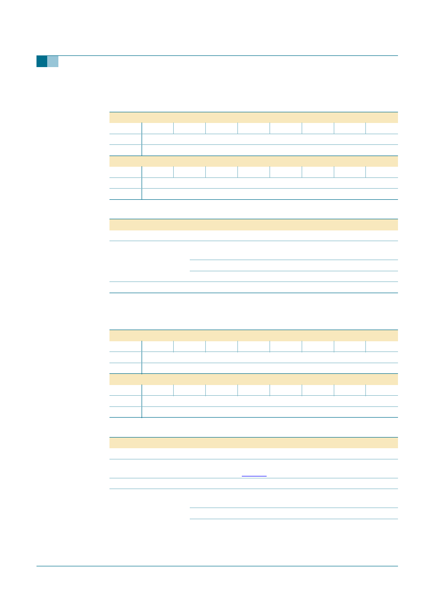
9397 750 14366
� Koninklijke Philips Electronics N.V. 2005. All rights reserved.
Product data sheet
Rev. 02 -- 17 January 2005
39 of 55
Philips Semiconductors
UDA1384
Multichannel audio coder-decoder
11.13 Supplemental settings 1
11.14 Supplemental settings 2
Table 58:
Supplemental settings 1 register (address 30h) bit allocation
Bit
15
14
13
12
11
10
9
8
Symbol
-
-
-
-
-
-
-
-
Reset
0
0
0
0
0
0
0
0
Access
read and write
Bit
7
6
5
4
3
2
1
0
Symbol
PDT
-
-
-
-
-
-
-
Reset
0
0
0
0
0
0
0
0
Access
read and write
Table 59:
Description of supplemental settings 1 register bits
Bit
Symbol
Description
15 to 8
-
default 0000 0000
7
PDT
Power down time. Bit PDT selects the time of the SDAC power-down
sequence.
1 = 1024/f
s
seconds
0 = 512/f
s
seconds (default)
6 to 0
-
default 000 0000
Table 60:
Supplemental settings 2 register (address 31h) bit allocation
Bit
15
14
13
12
11
10
9
8
Symbol
-
-
-
-
-
-
-
-
Reset
0
0
0
0
0
0
0
0
Access
read and write
Bit
7
6
5
4
3
2
1
0
Symbol
-
DITH2
DITH1
DITH0
-
-
VMTP
PDLNA
Reset
0
0
0
0
0
0
0
0
Access
read and write
Table 61:
Description of supplemental settings 2 register bits
Bit
Symbol
Description
15 to 7
-
default 0000 0000 0
6 to 4
DITH[2:0]
DAC dither control. A 3-bit value to control the dithering of the SDAC.
Default 000. See
Table 62
.
3 to 2
-
default 00
1
VMTP
Voice mute period control. Bit VMPT selects the voice ADC mute
period at power-up.
1 = mute for 1024 samples (1024/f
s
)
0 = mute for 2048 samples (2048/f
s
; default)

9397 750 14366
� Koninklijke Philips Electronics N.V. 2005. All rights reserved.
Product data sheet
Rev. 02 -- 17 January 2005
40 of 55
Philips Semiconductors
UDA1384
Multichannel audio coder-decoder
12. Limiting values
[1]
All supply connections must be made to the same power supply.
[2]
ESD behavior is tested in accordance with JEDEC II standard:
a) Human Body Model (HBM); equivalent to discharging a 100 pF capacitor through a 1.5 k
series
resistor.
b) Machine Model (MM); equivalent to discharging a 200 pF capacitor through a 0.75
�
H series inductor.
13. Thermal characteristics
0
PDLNA
Power-down voice LNA. Bit PDLNA is to power-down the voice ADC
LNA. It should be noted that disabling the LNA requires a recovery
time defined by the external RC circuit.
1 = power-down
0 = power-on (default)
Table 62:
DAC dither control bits
DITH2
DITH1
DITH0
Function
0
0
0
DC dither (mid level); default
0
0
1
reserved
0
1
0
reserved
0
1
1
reserved
1
0
0
DC dither (low level)
1
0
1
DC plus AC dither (low level)
1
1
0
DC dither (high level)
1
1
1
DC plus AC dither (high level)
Table 61:
Description of supplemental settings 2 register bits
...continued
Bit
Symbol
Description
Table 63:
Limiting values
In accordance with the Absolute Maximum Rating System (IEC 60134).
Symbol
Parameter
Conditions
Min
Max
Unit
V
DD
supply voltage
[1]
-
4.0
V
T
xtal(max)
maximum crystal
temperature
-
150
�
C
T
stg
storage temperature
-
65
+125
�
C
T
amb
ambient temperature
-
20
+85
�
C
V
esd
electrostatic discharge
voltage
HBM
[2]
-
2000
+2000
V
MM
[2]
-
200
+200
V
Table 64:
Thermal characteristics
Symbol
Parameter
Conditions
Typ
Unit
R
th(j-a)
thermal resistance from junction
to ambient
in free air
85
K/W

9397 750 14366
� Koninklijke Philips Electronics N.V. 2005. All rights reserved.
Product data sheet
Rev. 02 -- 17 January 2005
41 of 55
Philips Semiconductors
UDA1384
Multichannel audio coder-decoder
14. Static characteristics
Table 65:
Characteristics
V
DDD
= V
DDA(AD)
= V
DDA(DA)
= 3.3 V; T
amb
= 25
�
C; R
L
= 22 k
; all voltages referenced to ground (pins V
SS
); unless otherwise
specified.
Symbol
Parameter
Conditions
Min
Typ
Max
Unit
Supplies
V
DDA(AD)
ADC analog supply
voltage
[1]
2.7
3.3
3.6
V
V
DDA(DA)
DAC analog supply
voltage
[1]
2.7
3.3
3.6
V
V
DDD
digital supply voltage
[1]
2.7
3.3
3.6
V
I
DDA(AD)
ADC analog supply
current
f
ADC
= 48 kHz
-
30
-
mA
f
ADC
= 96 kHz
-
31
-
mA
I
DDA(DA)
DAC analog supply
current
f
DAC
= 48 kHz
-
20
-
mA
f
DAC
= 96 kHz
-
32
-
mA
I
DDD
digital supply current
f
ADC
= f
DAC
= 48 kHz;
f
VOICE
= 48 kHz
-
31
-
mA
f
ADC
= f
DAC
= 96 kHz;
f
VOICE
= 48 kHz
-
55
-
mA
I
DDD(pd)
digital supply current
in Power down-mode
audio and voice ADCs
power-down
-
18
-
mA
DAC power-down
-
14
-
mA
Digital input pins (5 V tolerant TTL compatible)
V
IH
HIGH-level input
voltage
2.0
-
-
V
V
IL
LOW-level input
voltage
-
-
0.8
V
I
LI
input leakage current
-
-
1
�
A
C
i
input capacitance
-
-
10
pF
Digital output pins
V
OH
HIGH-level output
voltage
I
OH
=
-
2 mA
0.85V
DDD
-
-
V
V
OL
LOW-level output
voltage
I
OL
= 2 mA
-
-
0.4
V
Analog-to-digital converter
V
ref
reference voltage on
pin V
ref
with respect to V
SSA(AD)
0.45V
DDA(AD)
0.5V
DDA(AD)
0.55V
DDA(AD)
V
V
ADCP
positive reference
voltage of ADC
-
V
DDA(AD)
-
V
V
ADCN
negative reference
voltage of ADC
0.0
0.0
0.0
V
R
o
output resistance on
pin V
ref
-
5
-
k
R
i(ADC)
input resistance of
audio ADC
-
10
-
k

9397 750 14366
� Koninklijke Philips Electronics N.V. 2005. All rights reserved.
Product data sheet
Rev. 02 -- 17 January 2005
42 of 55
Philips Semiconductors
UDA1384
Multichannel audio coder-decoder
[1]
All supply connections must be made to the same power supply unit.
15. Dynamic characteristics
R
i(VADC)
input resistance of
voice ADC
-
5
-
k
Digital-to-analog converter
R
L
load resistance
4
-
-
k
R
o
output resistance
-
1
-
k
Table 65:
Characteristics
...continued
V
DDD
= V
DDA(AD)
= V
DDA(DA)
= 3.3 V; T
amb
= 25
�
C; R
L
= 22 k
; all voltages referenced to ground (pins V
SS
); unless otherwise
specified.
Symbol
Parameter
Conditions
Min
Typ
Max
Unit
Table 66:
Characteristics
V
DDD
= V
DDA(AD)
= V
DDA(DA)
= 3.3 V; f
i
= 1 kHz; T
amb
= 25
�
C; R
L
= 22 k
; sampling frequency f
s
= 48 kHz; all voltages
referenced to ground (pins V
SS
); unless otherwise specified.
Symbol
Parameter
Conditions
Min
Typ
Max
Unit
Audio analog-to-digital converter
D
0
digital output level
at 0 dB setting; 900 mV input
[1] [2]
-
2.5
-
1.2
-
0.7
dB
at 3 dB setting; 637 mV input
[2]
-
-
1.2
-
dB
at 6 dB setting; 451 mV input
[2]
-
-
1.2
-
dB
at 9 dB setting; 319 mV input
[2]
-
-
1.2
-
dB
at 12 dB setting; 226 mV input
[2]
-
-
1.2
-
dB
at 15 dB setting; 160 mV input
[2]
-
-
1.2
-
dB
at 18 dB setting; 113 mV input
[2]
-
-
1.2
-
dB
at 21 dB setting; 80 mV input
[2]
-
-
1.2
-
dB
at 24 dB setting; 57 mV input
[2]
-
-
1.2
-
dB
V
i
input voltage unbalance between
channels
-
0.1
-
dB

9397 750 14366
� Koninklijke Philips Electronics N.V. 2005. All rights reserved.
Product data sheet
Rev. 02 -- 17 January 2005
43 of 55
Philips Semiconductors
UDA1384
Multichannel audio coder-decoder
(THD + N)/S total harmonic
distortion-plus-noise to signal ratio
normal mode; at
-
1 dBFS
at 0 dB setting
-
-
88
-
82
dB
at 3 dB setting
-
-
88
-
dB
at 6 dB setting
-
-
88
-
dB
at 9 dB setting
-
-
88
-
dB
at 12 dB setting
-
-
88
-
dB
at 15 dB setting
-
-
87
-
dB
at 18 dB setting
-
-
85
-
dB
at 21 dB setting
-
-
83
-
dB
at 24 dB setting
-
-
82
-
dB
normal mode; at
-
60 dBFS;
A-weighted
at 0 dB setting
-
-
37
-
30
dB
at 3 dB setting
-
-
37
-
dB
at 6 dB setting
-
-
37
-
dB
at 9 dB setting
-
-
37
-
dB
at 12 dB setting
-
-
37
-
dB
at 15 dB setting
-
-
37
-
dB
at 18 dB setting
-
-
35
-
dB
at 21 dB setting
-
-
32
-
dB
at 24 dB setting
-
-
30
-
dB
S/N
signal-to-noise ratio
code = 0; A-weighted
89
98
-
dB
cs
channel separation
-
100
-
dB
Voice analog-to-digital converter
V
i(rms)
input voltage (RMS value)
at 0 dBFS digital output; 2.2 k
source impedance
-
50.0
-
mV
(THD + N)/S total harmonic
distortion-plus-noise to signal ratio
at
-
1 dBFS
-
-
78
-
dB
at
-
20 dBFS
-
-
65
-
dB
at
-
40 dBFS; A-weighted
-
-
47
-
dB
S/N
signal-to-noise ratio
code = 0; A-weighted
-
87
-
dB
Digital-to-analog converter
Differential mode
V
o(rms)
output voltage (RMS value)
at 0 dBFS digital input
1.9
2.0
2.1
V
V
o
output voltage unbalance between
channels
-
< 0.1
-
dB
(THD + N)/S total harmonic
distortion-plus-noise to signal ratio
at 0 dBFS
-
-
98
-
93
dB
at
-
20 dBFS
-
-
90
-
dB
at
-
60 dBFS; A-weighted
-
-
50
-
45
dB
S/N
signal-to-noise ratio
code = 0; A-weighted
100
110
-
dB
cs
channel separation
-
114
-
dB
Table 66:
Characteristics
...continued
V
DDD
= V
DDA(AD)
= V
DDA(DA)
= 3.3 V; f
i
= 1 kHz; T
amb
= 25
�
C; R
L
= 22 k
; sampling frequency f
s
= 48 kHz; all voltages
referenced to ground (pins V
SS
); unless otherwise specified.
Symbol
Parameter
Conditions
Min
Typ
Max
Unit

9397 750 14366
� Koninklijke Philips Electronics N.V. 2005. All rights reserved.
Product data sheet
Rev. 02 -- 17 January 2005
44 of 55
Philips Semiconductors
UDA1384
Multichannel audio coder-decoder
[1]
The input voltage can be up to 2 V (RMS) when the current through the ADC input pin is limited to approximately 1 mA by using a series
resistor.
[2]
The input voltage to the ADC scales proportionally with the power supply voltage.
15.1 Timing
Single-ended mode
V
o(rms)
output voltage (RMS value)
at 0 dBFS digital input
-
1.0
-
V
V
o
output voltage unbalance between
channels
-
< 0.1
-
dB
(THD + N)/S total harmonic
distortion-plus-noise to signal ratio
at 0 dBFS
-
-
88
-
dB
at
-
20 dBFS
-
-
85
-
dB
at
-
60 dBFS; A-weighted
-
-
45
-
dB
S/N
signal-to-noise ratio
code = 0; A-weighted
-
105
-
dB
cs
channel separation
-
110
-
dB
Table 66:
Characteristics
...continued
V
DDD
= V
DDA(AD)
= V
DDA(DA)
= 3.3 V; f
i
= 1 kHz; T
amb
= 25
�
C; R
L
= 22 k
; sampling frequency f
s
= 48 kHz; all voltages
referenced to ground (pins V
SS
); unless otherwise specified.
Symbol
Parameter
Conditions
Min
Typ
Max
Unit
Table 67:
Timing
V
DDD
= V
DDA(AD)
= V
DDA(AD)
= 2.7 V to 3.6 V; T
amb
=
-
20
�
C to +85
�
C; typical timing specified at sampling frequency
f
s
= 48 kHz; unless otherwise specified.
Symbol
Parameter
Conditions
Min
Typ
Max
Unit
System clock (see
Figure 16
)
T
sys
system clock cycle time
f
sys
= 256f
s
[1]
35
81
780
ns
f
sys
= 384f
s
[1]
23
54
520
ns
f
sys
= 512f
s
[1]
17
41
390
ns
f
sys
= 768f
s
[1]
17
27
260
ns
t
CWL
system clock LOW time
f
sys
< 19.2 MHz
0.3T
sys
-
0.7T
sys
ns
f
sys
19.2 MHz
0.4T
sys
-
0.6T
sys
ns
t
CWH
system clock HIGH time
f
sys
< 19.2 MHz
0.3T
sys
-
0.7T
sys
ns
f
sys
19.2 MHz
0.4T
sys
-
0.6T
sys
ns
I
2
S-bus interface
Serial data of audio ADC and DAC (see
Figure 17
)
f
BCK
audio bit clock frequency
[2]
-
-
12.8
MHz
T
cy(BCK)
BCK cycle time
-
-
78
ns
t
BCKH
bit clock HIGH time
30
-
-
ns
t
BCKL
bit clock LOW time
30
-
-
ns
t
r
rise time
-
-
20
ns
t
f
fall time
-
-
20
ns
t
su(WS)
word select set-up time
10
-
-
ns
t
h(WS)
word select hold time
10
-
-
ns
t
su(DATAI)
data input set-up time
10
-
-
ns
t
h(DATAI)
data input hold time
10
-
-
ns
t
h(DATAO)
data output hold time
0
-
-
ns

9397 750 14366
� Koninklijke Philips Electronics N.V. 2005. All rights reserved.
Product data sheet
Rev. 02 -- 17 January 2005
45 of 55
Philips Semiconductors
UDA1384
Multichannel audio coder-decoder
t
d(DATAO-BCK)
data output to bit clock delay
-
-
30
ns
t
d(DATAO-WS)
data output to word select
delay
-
-
30
ns
Serial data of voice ADC
f
BCKV
voice bit clock frequency
[2]
-
-
6.4
MHz
T
cy(BCKV)
BCKV cycle time
-
-
156
ns
t
BCKVH
bit clock HIGH time
50
-
-
ns
t
BCKVL
bit clock LOW time
50
-
-
ns
t
r
rise time
-
-
20
ns
t
f
fall time
-
-
20
ns
t
su(WSV)
word select set-up time
10
-
-
ns
t
h(WSV)
word select hold time
10
-
-
ns
t
h(DATAV)
data output hold time
0
-
-
ns
t
d(DATAV-BCKV)
data output to bit clock delay
-
-
30
ns
t
d(DATAV-WSV)
data output to word select
delay
-
-
30
ns
t
d(WSV-BCKV)
word select to bit clock delay WSV-out mode
-
30
-
+30
ns
L3-bus interface (see
Figure 18
and
Figure 19
)
L3CLOCK timing
f
cy(CLK)L3
L3CLOCK frequency
-
-
2000
kHz
T
cy(CLK)L3
L3CLOCK cycle time
500
-
-
ns
t
CLK(L3)H
L3CLOCK HIGH time
250
-
-
ns
t
CLK(L3)L
L3CLOCK LOW time
250
-
-
ns
L3MODE timing
t
su(L3)A
L3MODE set-up time in
address mode
190
-
-
ns
t
h(L3)A
L3MODE hold time in
address mode
190
-
-
ns
t
su(L3)D
L3MODE set-up time in data
transfer mode
190
-
-
ns
t
h(L3)D
L3MODE hold time in data
transfer mode
190
-
-
ns
t
stp(L3)
L3MODE stop time in data
transfer mode
190
-
-
ns
L3DATA timing
t
su(L3)DA
L3DATA set-up time in data
transfer and address mode
190
-
-
ns
t
h(L3)DA
L3DATA hold time in data
transfer and address mode
30
-
-
ns
t
d(L3)R
L3DATA delay time for read
data
0
-
50
ns
Table 67:
Timing
...continued
V
DDD
= V
DDA(AD)
= V
DDA(AD)
= 2.7 V to 3.6 V; T
amb
=
-
20
�
C to +85
�
C; typical timing specified at sampling frequency
f
s
= 48 kHz; unless otherwise specified.
Symbol
Parameter
Conditions
Min
Typ
Max
Unit

9397 750 14366
� Koninklijke Philips Electronics N.V. 2005. All rights reserved.
Product data sheet
Rev. 02 -- 17 January 2005
46 of 55
Philips Semiconductors
UDA1384
Multichannel audio coder-decoder
[1]
The system clock should not exceed 58 MHz in any mode.
[2]
The bit clock frequency should not exceed 256 times the corresponding sampling frequency.
[3]
C
b
is the total capacitance for each bus line.
[4]
To be suppressed by the input filter.
t
dis(L3)R
L3DATA disable time for read
data
0
-
50
ns
I
2
C-bus interface timing (see
Figure 20
)
SCL timing
f
SCL
SCL clock frequency
0
-
400
kHz
t
LOW
SCL LOW time
1.3
-
-
�
s
t
HIGH
SCL HIGH time
0.6
-
-
�
s
t
r
rise time SDA and SCL
[3]
20 + 0.1C
b
-
300
ns
t
f
fall time SDA and SCL
[3]
20 + 0.1C
b
-
300
ns
SDA timing
t
BUF
bus free time between STOP
and START condition
1.3
-
-
�
s
t
SU;STA
set-up time repeated START
0.6
-
-
�
s
t
HD;STA
hold time START condition
0.6
-
-
�
s
t
SU;DAT
data set-up time
100
-
-
ns
t
HD;DAT
data hold time
0
-
-
�
s
t
SU;STO
set-up time STOP condition
0.6
-
-
�
s
t
SP
pulse width of spikes
[4]
0
-
50
ns
C
b
capacitive load for each bus
line
-
-
400
pF
Table 67:
Timing
...continued
V
DDD
= V
DDA(AD)
= V
DDA(AD)
= 2.7 V to 3.6 V; T
amb
=
-
20
�
C to +85
�
C; typical timing specified at sampling frequency
f
s
= 48 kHz; unless otherwise specified.
Symbol
Parameter
Conditions
Min
Typ
Max
Unit
Fig 16. System clock timing
mgr984
T
sys
t
CWH
t
CWL
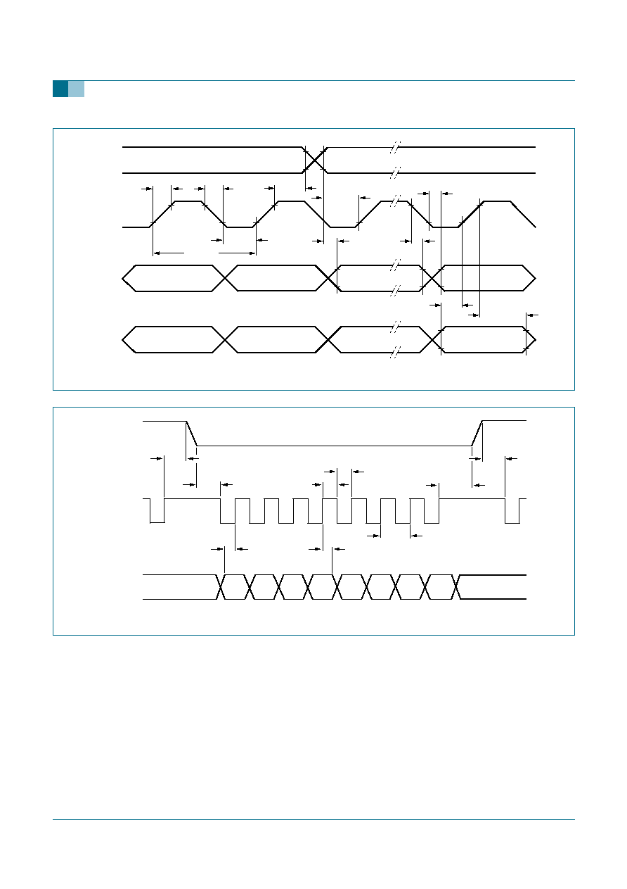
9397 750 14366
� Koninklijke Philips Electronics N.V. 2005. All rights reserved.
Product data sheet
Rev. 02 -- 17 January 2005
47 of 55
Philips Semiconductors
UDA1384
Multichannel audio coder-decoder
Fig 17. I
2
S-bus serial interface timing
mgs756
WS
BCK
DATAO
DATAI
t
f
t
r
t
h(WS)
t
su(WS)
t
BCKH
t
BCKL
T
cy(BCK)
t
h(DATAO)
t
su(DATAI)
t
h(DATAI)
t
d(DATAO-BCK)
t
d(DATAO-WS)
Fig 18. L3-bus address mode timing
t
h(L3)A
t
h(L3)DA
t
su(L3)DA
T
cy(CLK)(L3)
BIT 0
L3MODE
L3CLOCK
L3DATA
BIT 7
mgl723
t
CLK(L3)H
t
CLK(L3)L
t
su(L3)A
t
su(L3)A
t
h(L3)A
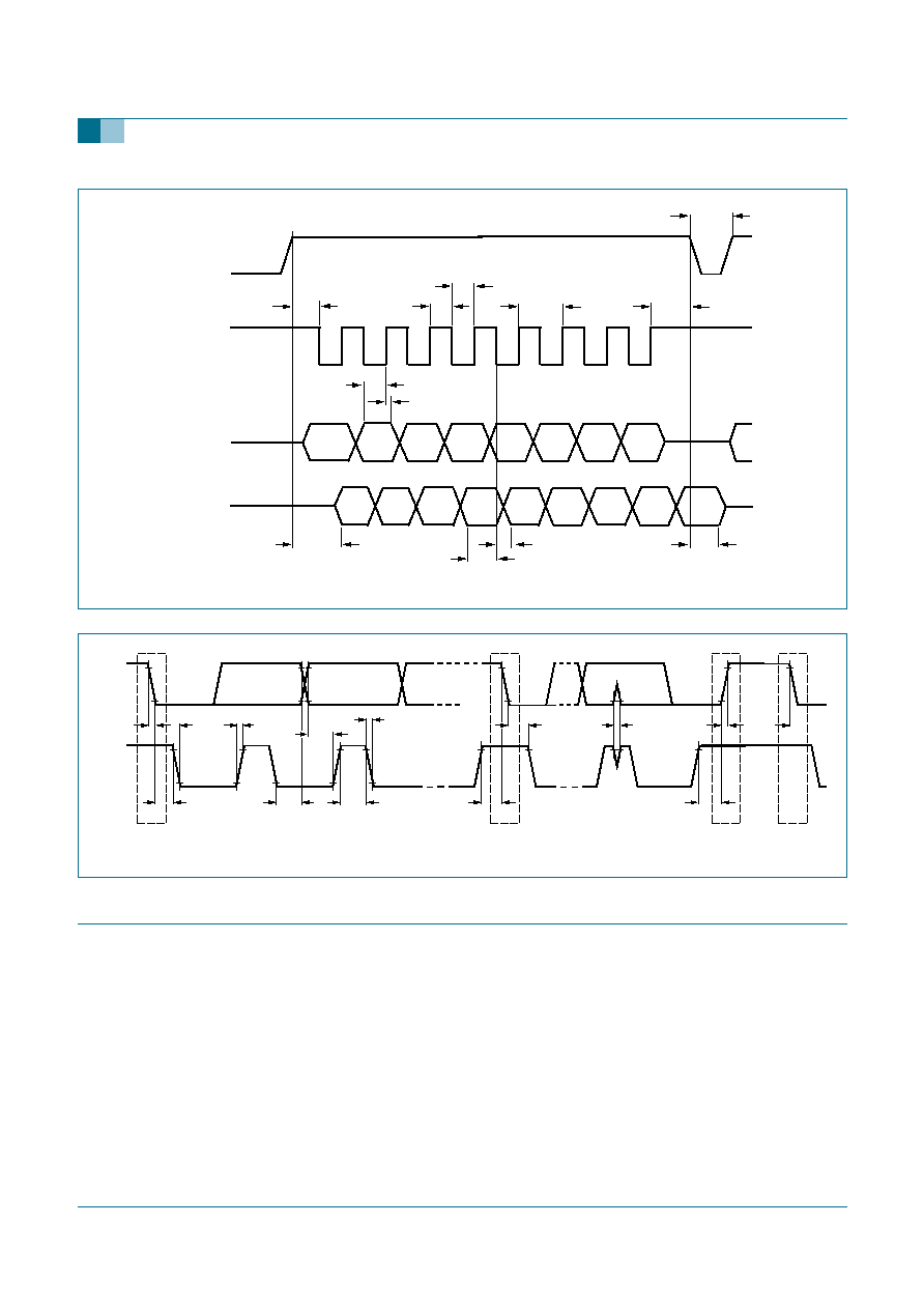
9397 750 14366
� Koninklijke Philips Electronics N.V. 2005. All rights reserved.
Product data sheet
Rev. 02 -- 17 January 2005
48 of 55
Philips Semiconductors
UDA1384
Multichannel audio coder-decoder
16. Test information
16.1 Quality information
The
General Quality Specification for Integrated Circuits, SNW-FQ-611 is applicable.
Fig 19. L3-bus data transfer (write and read) mode timing
t
stp(L3)
t
su(L3)D
t
h(L3)DA
t
en(L3)R
t
h(L3)R
t
su(L3)DA
t
h(L3)D
T
cy(CLK)L3
BIT 0
L3MODE
L3CLOCK
L3DATA
read
L3DATA
write
BIT 7
mgu015
t
CLK(L3)H
t
CLK(L3)L
t
su(L3)R
t
dis(L3)R
Fig 20. I
2
C-bus timing
msc610
S
Sr
t
SU;STO
t
SU;STA
t
HD;STA
t
HIGH
t
LOW
t
SU;DAT
t
HD;DAT
t
f
SDA
SCL
P
S
t
BUF
t
r
t
f
t
r
t
SP
t
HD;STA
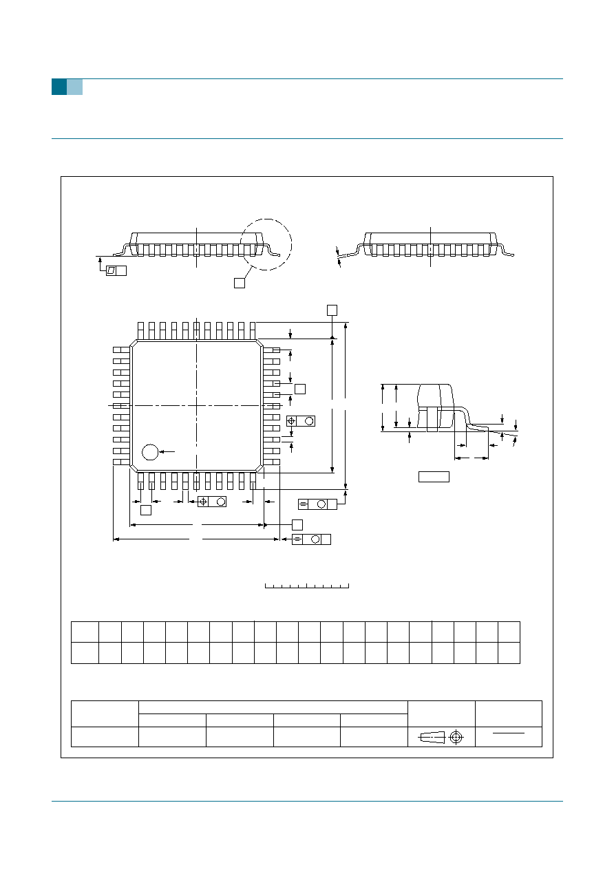
9397 750 14366
� Koninklijke Philips Electronics N.V. 2005. All rights reserved.
Product data sheet
Rev. 02 -- 17 January 2005
49 of 55
Philips Semiconductors
UDA1384
Multichannel audio coder-decoder
17. Package outline
Fig 21. Package outline SOT307-2 (QFP44)
UNIT
A
1
A
2
A
3
b
p
c
E
(1)
e
H
E
L
L
p
Z
y
w
v
REFERENCES
OUTLINE
VERSION
EUROPEAN
PROJECTION
ISSUE DATE
IEC
JEDEC
JEITA
mm
0.25
0.05
1.85
1.65
0.25
0.4
0.2
0.25
0.14
10.1
9.9
0.8
1.3
12.9
12.3
1.2
0.8
10
0
o
o
0.15
0.1
0.15
DIMENSIONS (mm are the original dimensions)
Note
1. Plastic or metal protrusions of 0.25 mm maximum per side are not included.
0.95
0.55
SOT307-2
97-08-01
03-02-25
D
(1)
(1)
(1)
10.1
9.9
H
D
12.9
12.3
E
Z
1.2
0.8
D
e
E
B
11
c
E
H
D
ZD
A
Z E
e
v
M
A
X
1
44
34
33
23
22
12
y
A
1
A
L
p
detail X
L
(A )
3
A
2
pin 1 index
D
H
v
M
B
b
p
b
p
w
M
w
M
0
2.5
5 mm
scale
QFP44: plastic quad flat package; 44 leads (lead length 1.3 mm); body 10 x 10 x 1.75 mm
SOT307-2
A
max.
2.1

9397 750 14366
� Koninklijke Philips Electronics N.V. 2005. All rights reserved.
Product data sheet
Rev. 02 -- 17 January 2005
50 of 55
Philips Semiconductors
UDA1384
Multichannel audio coder-decoder
18. Handling information
Inputs and outputs are protected against electrostatic discharge in normal handling.
However, to be completely safe, it is desirable to take normal precautions appropriate to
handling integrated circuits.
19. Soldering
19.1 Introduction to soldering surface mount packages
This text gives a very brief insight to a complex technology. A more in-depth account of
soldering ICs can be found in our
Data Handbook IC26; Integrated Circuit Packages
(document order number 9398 652 90011).
There is no soldering method that is ideal for all surface mount IC packages. Wave
soldering can still be used for certain surface mount ICs, but it is not suitable for fine pitch
SMDs. In these situations reflow soldering is recommended.
19.2 Reflow soldering
Reflow soldering requires solder paste (a suspension of fine solder particles, flux and
binding agent) to be applied to the printed-circuit board by screen printing, stencilling or
pressure-syringe dispensing before package placement. Driven by legislation and
environmental forces the worldwide use of lead-free solder pastes is increasing.
Several methods exist for reflowing; for example, convection or convection/infrared
heating in a conveyor type oven. Throughput times (preheating, soldering and cooling)
vary between 100 seconds and 200 seconds depending on heating method.
Typical reflow peak temperatures range from 215
�
C to 270
�
C depending on solder paste
material. The top-surface temperature of the packages should preferably be kept:
�
below 225
�
C (SnPb process) or below 245
�
C (Pb-free process)
� for all BGA, HTSSON..T and SSOP..T packages
� for packages with a thickness
2.5 mm
� for packages with a thickness < 2.5 mm and a volume
350 mm
3
so called
thick/large packages.
�
below 240
�
C (SnPb process) or below 260
�
C (Pb-free process) for packages with a
thickness < 2.5 mm and a volume < 350 mm
3
so called small/thin packages.
Moisture sensitivity precautions, as indicated on packing, must be respected at all times.
19.3 Wave soldering
Conventional single wave soldering is not recommended for surface mount devices
(SMDs) or printed-circuit boards with a high component density, as solder bridging and
non-wetting can present major problems.
To overcome these problems the double-wave soldering method was specifically
developed.
If wave soldering is used the following conditions must be observed for optimal results:

9397 750 14366
� Koninklijke Philips Electronics N.V. 2005. All rights reserved.
Product data sheet
Rev. 02 -- 17 January 2005
51 of 55
Philips Semiconductors
UDA1384
Multichannel audio coder-decoder
�
Use a double-wave soldering method comprising a turbulent wave with high upward
pressure followed by a smooth laminar wave.
�
For packages with leads on two sides and a pitch (e):
� larger than or equal to 1.27 mm, the footprint longitudinal axis is preferred to be
parallel to the transport direction of the printed-circuit board;
� smaller than 1.27 mm, the footprint longitudinal axis must be parallel to the
transport direction of the printed-circuit board.
The footprint must incorporate solder thieves at the downstream end.
�
For packages with leads on four sides, the footprint must be placed at a 45
�
angle to
the transport direction of the printed-circuit board. The footprint must incorporate
solder thieves downstream and at the side corners.
During placement and before soldering, the package must be fixed with a droplet of
adhesive. The adhesive can be applied by screen printing, pin transfer or syringe
dispensing. The package can be soldered after the adhesive is cured.
Typical dwell time of the leads in the wave ranges from 3 seconds to 4 seconds at 250
�
C
or 265
�
C, depending on solder material applied, SnPb or Pb-free respectively.
A mildly-activated flux will eliminate the need for removal of corrosive residues in most
applications.
19.4 Manual soldering
Fix the component by first soldering two diagonally-opposite end leads. Use a low voltage
(24 V or less) soldering iron applied to the flat part of the lead. Contact time must be
limited to 10 seconds at up to 300
�
C.
When using a dedicated tool, all other leads can be soldered in one operation within
2 seconds to 5 seconds between 270
�
C and 320
�
C.
19.5 Package related soldering information
[1]
For more detailed information on the BGA packages refer to the
(LF)BGA Application Note (AN01026);
order a copy from your Philips Semiconductors sales office.
Table 68:
Suitability of surface mount IC packages for wave and reflow soldering methods
Package
[1]
Soldering method
Wave
Reflow
[2]
BGA, HTSSON..T
[3]
, LBGA, LFBGA, SQFP,
SSOP..T
[3]
, TFBGA, VFBGA, XSON
not suitable
suitable
DHVQFN, HBCC, HBGA, HLQFP, HSO, HSOP,
HSQFP, HSSON, HTQFP, HTSSOP, HVQFN,
HVSON, SMS
not suitable
[4]
suitable
PLCC
[5]
, SO, SOJ
suitable
suitable
LQFP, QFP, TQFP
not recommended
[5] [6]
suitable
SSOP, TSSOP, VSO, VSSOP
not recommended
[7]
suitable
CWQCCN..L
[8]
, PMFP
[9]
, WQCCN..L
[8]
not suitable
not suitable

9397 750 14366
� Koninklijke Philips Electronics N.V. 2005. All rights reserved.
Product data sheet
Rev. 02 -- 17 January 2005
52 of 55
Philips Semiconductors
UDA1384
Multichannel audio coder-decoder
[2]
All surface mount (SMD) packages are moisture sensitive. Depending upon the moisture content, the
maximum temperature (with respect to time) and body size of the package, there is a risk that internal or
external package cracks may occur due to vaporization of the moisture in them (the so called popcorn
effect). For details, refer to the Drypack information in the
Data Handbook IC26; Integrated Circuit
Packages; Section: Packing Methods.
[3]
These transparent plastic packages are extremely sensitive to reflow soldering conditions and must on no
account be processed through more than one soldering cycle or subjected to infrared reflow soldering with
peak temperature exceeding 217
�
C
�
10
�
C measured in the atmosphere of the reflow oven. The package
body peak temperature must be kept as low as possible.
[4]
These packages are not suitable for wave soldering. On versions with the heatsink on the bottom side, the
solder cannot penetrate between the printed-circuit board and the heatsink. On versions with the heatsink
on the top side, the solder might be deposited on the heatsink surface.
[5]
If wave soldering is considered, then the package must be placed at a 45
�
angle to the solder wave
direction. The package footprint must incorporate solder thieves downstream and at the side corners.
[6]
Wave soldering is suitable for LQFP, QFP and TQFP packages with a pitch (e) larger than 0.8 mm; it is
definitely not suitable for packages with a pitch (e) equal to or smaller than 0.65 mm.
[7]
Wave soldering is suitable for SSOP, TSSOP, VSO and VSSOP packages with a pitch (e) equal to or larger
than 0.65 mm; it is definitely not suitable for packages with a pitch (e) equal to or smaller than 0.5 mm.
[8]
Image sensor packages in principle should not be soldered. They are mounted in sockets or delivered
pre-mounted on flex foil. However, the image sensor package can be mounted by the client on a flex foil by
using a hot bar soldering process. The appropriate soldering profile can be provided on request.
[9]
Hot bar soldering or manual soldering is suitable for PMFP packages.

9397 750 14366
� Koninklijke Philips Electronics N.V. 2005. All rights reserved.
Product data sheet
Rev. 02 -- 17 January 2005
53 of 55
Philips Semiconductors
UDA1384
Multichannel audio coder-decoder
20. Revision history
Table 69:
Revision history
Document ID
Release date
Data sheet status
Change notice
Doc. number
Supersedes
UDA1384_2
20050117
Product data sheet
-
9397 750 14366
UDA1384_1
Modifications:
�
The format of this data sheet has been redesigned to comply with the new presentation and
information standard of Philips Semiconductors
�
Section 4 "Quick reference data"
: Added values for I
DDD(pd)
�
Section 14 "Static characteristics"
: Added values for I
DDD(pd)
�
Section 15 "Dynamic characteristics"
: Removed PSRR specification and (THD+N)/S at
-
20 dBFS, added (THD+N)/S for DAC differential mode
UDA1384_1
20031009
Preliminary specification -
9397 750 12043
-

Philips Semiconductors
UDA1384
Multichannel audio coder-decoder
9397 750 14366
� Koninklijke Philips Electronics N.V. 2005. All rights reserved.
Product data sheet
Rev. 02 -- 17 January 2005
54 of 55
21. Data sheet status
[1]
Please consult the most recently issued data sheet before initiating or completing a design.
[2]
The product status of the device(s) described in this data sheet may have changed since this data sheet was published. The latest information is available on the Internet at
URL http://www.semiconductors.philips.com.
[3]
For data sheets describing multiple type numbers, the highest-level product status determines the data sheet status.
22. Definitions
Short-form specification -- The data in a short-form specification is
extracted from a full data sheet with the same type number and title. For
detailed information see the relevant data sheet or data handbook.
Limiting values definition -- Limiting values given are in accordance with
the Absolute Maximum Rating System (IEC 60134). Stress above one or
more of the limiting values may cause permanent damage to the device.
These are stress ratings only and operation of the device at these or at any
other conditions above those given in the Characteristics sections of the
specification is not implied. Exposure to limiting values for extended periods
may affect device reliability.
Application information -- Applications that are described herein for any
of these products are for illustrative purposes only. Philips Semiconductors
make no representation or warranty that such applications will be suitable for
the specified use without further testing or modification.
23. Disclaimers
Life support -- These products are not designed for use in life support
appliances, devices, or systems where malfunction of these products can
reasonably be expected to result in personal injury. Philips Semiconductors
customers using or selling these products for use in such applications do so
at their own risk and agree to fully indemnify Philips Semiconductors for any
damages resulting from such application.
Right to make changes -- Philips Semiconductors reserves the right to
make changes in the products - including circuits, standard cells, and/or
software - described or contained herein in order to improve design and/or
performance. When the product is in full production (status `Production'),
relevant changes will be communicated via a Customer Product/Process
Change Notification (CPCN). Philips Semiconductors assumes no
responsibility or liability for the use of any of these products, conveys no
license or title under any patent, copyright, or mask work right to these
products, and makes no representations or warranties that these products are
free from patent, copyright, or mask work right infringement, unless otherwise
specified.
24. Contact information
For additional information, please visit: http://www.semiconductors.philips.com
For sales office addresses, send an email to: sales.addresses@www.semiconductors.philips.com
Level
Data sheet status
[1]
Product status
[2] [3]
Definition
I
Objective data
Development
This data sheet contains data from the objective specification for product development. Philips
Semiconductors reserves the right to change the specification in any manner without notice.
II
Preliminary data
Qualification
This data sheet contains data from the preliminary specification. Supplementary data will be published
at a later date. Philips Semiconductors reserves the right to change the specification without notice, in
order to improve the design and supply the best possible product.
III
Product data
Production
This data sheet contains data from the product specification. Philips Semiconductors reserves the
right to make changes at any time in order to improve the design, manufacturing and supply. Relevant
changes will be communicated via a Customer Product/Process Change Notification (CPCN).

� Koninklijke Philips Electronics N.V. 2005
All rights are reserved. Reproduction in whole or in part is prohibited without the prior
written consent of the copyright owner. The information presented in this document does
not form part of any quotation or contract, is believed to be accurate and reliable and may
be changed without notice. No liability will be accepted by the publisher for any
consequence of its use. Publication thereof does not convey nor imply any license under
patent- or other industrial or intellectual property rights.
Date of release: 17 January 2005
Document number: 9397 750 14366
Published in The Netherlands
Philips Semiconductors
UDA1384
Multichannel audio coder-decoder
25. Contents
1
General description . . . . . . . . . . . . . . . . . . . . . . 1
2
Features . . . . . . . . . . . . . . . . . . . . . . . . . . . . . . . 1
2.1
General . . . . . . . . . . . . . . . . . . . . . . . . . . . . . . . 1
2.2
Multiple format data interface . . . . . . . . . . . . . . 2
2.3
Digital sound processing. . . . . . . . . . . . . . . . . . 2
2.4
Advanced audio configuration . . . . . . . . . . . . . 2
3
Applications . . . . . . . . . . . . . . . . . . . . . . . . . . . . 2
4
Quick reference data . . . . . . . . . . . . . . . . . . . . . 2
5
Ordering information . . . . . . . . . . . . . . . . . . . . . 3
6
Block diagram . . . . . . . . . . . . . . . . . . . . . . . . . . 4
7
Pinning information . . . . . . . . . . . . . . . . . . . . . . 5
7.1
Pinning . . . . . . . . . . . . . . . . . . . . . . . . . . . . . . . 5
7.2
Pin description . . . . . . . . . . . . . . . . . . . . . . . . . 5
8
Functional description . . . . . . . . . . . . . . . . . . . 7
8.1
System clock. . . . . . . . . . . . . . . . . . . . . . . . . . . 7
8.2
Audio analog-to-digital converter (audio ADC) . 8
8.3
Voice Analog-to-Digital Converter (voice ADC) 8
8.4
Decimation filter of audio ADC . . . . . . . . . . . . . 8
8.5
Decimation filter of voice ADC . . . . . . . . . . . . . 8
8.6
Interpolation filter of DAC . . . . . . . . . . . . . . . . . 9
8.7
Noise shaper of DAC . . . . . . . . . . . . . . . . . . . . 9
8.8
Digital mixer . . . . . . . . . . . . . . . . . . . . . . . . . . . 9
8.9
Audio digital-to-analog converters . . . . . . . . . 10
8.10
Power-on reset . . . . . . . . . . . . . . . . . . . . . . . . 10
8.11
Audio digital interface . . . . . . . . . . . . . . . . . . . 11
8.12
Voice digital interface . . . . . . . . . . . . . . . . . . . 14
8.13
DSD mode . . . . . . . . . . . . . . . . . . . . . . . . . . . 14
8.14
Microcontroller interface mode . . . . . . . . . . . . 15
9
L3-bus interface . . . . . . . . . . . . . . . . . . . . . . . . 15
9.1
General . . . . . . . . . . . . . . . . . . . . . . . . . . . . . . 15
9.2
Device addressing . . . . . . . . . . . . . . . . . . . . . 16
9.3
Register addressing . . . . . . . . . . . . . . . . . . . . 16
9.4
Data write mode . . . . . . . . . . . . . . . . . . . . . . . 18
9.5
Data read mode . . . . . . . . . . . . . . . . . . . . . . . 18
10
I
2
C-bus interface . . . . . . . . . . . . . . . . . . . . . . . 19
10.1
General . . . . . . . . . . . . . . . . . . . . . . . . . . . . . . 19
10.2
Characteristics of the I
2
C-bus . . . . . . . . . . . . . 19
10.3
Bit transfer . . . . . . . . . . . . . . . . . . . . . . . . . . . 19
10.4
Byte transfer . . . . . . . . . . . . . . . . . . . . . . . . . . 20
10.5
Data transfer . . . . . . . . . . . . . . . . . . . . . . . . . . 20
10.6
Start and stop conditions . . . . . . . . . . . . . . . . 20
10.7
Acknowledgment . . . . . . . . . . . . . . . . . . . . . . 20
10.8
Device address . . . . . . . . . . . . . . . . . . . . . . . . 21
10.9
Register address. . . . . . . . . . . . . . . . . . . . . . . 21
10.10
Write and read data . . . . . . . . . . . . . . . . . . . . 21
10.11
Write cycle . . . . . . . . . . . . . . . . . . . . . . . . . . . 22
10.12
Read cycle . . . . . . . . . . . . . . . . . . . . . . . . . . . 22
11
Register mapping . . . . . . . . . . . . . . . . . . . . . . 23
11.1
Address mapping . . . . . . . . . . . . . . . . . . . . . . 23
11.2
Register mapping . . . . . . . . . . . . . . . . . . . . . . 25
11.3
System settings . . . . . . . . . . . . . . . . . . . . . . . 27
11.4
Audio ADC and DAC subsystem settings. . . . 29
11.5
Voice ADC system settings . . . . . . . . . . . . . . 30
11.6
Status output register . . . . . . . . . . . . . . . . . . . 32
11.7
DAC channel selection . . . . . . . . . . . . . . . . . . 33
11.8
DAC features settings. . . . . . . . . . . . . . . . . . . 34
11.9
DAC channel 1 to channel 6 settings . . . . . . . 36
11.10
DAC mixing channel settings . . . . . . . . . . . . . 36
11.11
Audio ADC 1 and ADC 2 input amplifier gain
settings. . . . . . . . . . . . . . . . . . . . . . . . . . . . . . 37
11.12
Voice ADC gain settings. . . . . . . . . . . . . . . . . 38
11.13
Supplemental settings 1. . . . . . . . . . . . . . . . . 39
11.14
Supplemental settings 2. . . . . . . . . . . . . . . . . 39
12
Limiting values . . . . . . . . . . . . . . . . . . . . . . . . 40
13
Thermal characteristics . . . . . . . . . . . . . . . . . 40
14
Static characteristics . . . . . . . . . . . . . . . . . . . 41
15
Dynamic characteristics . . . . . . . . . . . . . . . . . 42
15.1
Timing . . . . . . . . . . . . . . . . . . . . . . . . . . . . . . 44
16
Test information. . . . . . . . . . . . . . . . . . . . . . . . 48
16.1
Quality information . . . . . . . . . . . . . . . . . . . . . 48
17
Package outline . . . . . . . . . . . . . . . . . . . . . . . . 49
18
Handling information . . . . . . . . . . . . . . . . . . . 50
19
Soldering . . . . . . . . . . . . . . . . . . . . . . . . . . . . . 50
19.1
Introduction to soldering surface mount packages
50
19.2
Reflow soldering. . . . . . . . . . . . . . . . . . . . . . . 50
19.3
Wave soldering. . . . . . . . . . . . . . . . . . . . . . . . 50
19.4
Manual soldering . . . . . . . . . . . . . . . . . . . . . . 51
19.5
Package related soldering information . . . . . . 51
20
Revision history . . . . . . . . . . . . . . . . . . . . . . . 53
21
Data sheet status. . . . . . . . . . . . . . . . . . . . . . . 54
22
Definitions . . . . . . . . . . . . . . . . . . . . . . . . . . . . 54
23
Disclaimers . . . . . . . . . . . . . . . . . . . . . . . . . . . 54
24
Licenses . . . . . . . . . . . . . . . . . . . . . . . . . . . . . . 54
25
Contact information . . . . . . . . . . . . . . . . . . . . 54