
1.
General description
The UJA1061 fail-safe System Basis Chip (fail-safe SBC) replaces basic discrete
components which are common in every Electronic Control Unit (ECU) with a Controller
Area Network (CAN) and a Local Interconnect Network (LIN) interface. The fail-safe SBC
supports all networking applications which control various power and sensor peripherals
by using fault-tolerant CAN as the main network interface and LIN as a local sub-bus. The
fail-safe SBC contains the following integrated devices:
�
ISO11898-3 compliant fault-tolerant CAN transceiver, interoperable with TJA1054,
TJA1054A and TJA1055
�
LIN transceiver compliant with LIN 2.0 and SAE J2602, and compatible with LIN 1.3
�
Advanced independant watchdog
�
Dedicated voltage regulators for microcontroller and CAN transceiver
�
Serial peripheral interface (full duplex)
�
Local wake-up input port
�
Inhibit / limp home output port
In addition to the advantages of integrating these common ECU functions in a single
package, the fail-safe SBC offers an intelligent combination of system-specific functions
such as:
�
Advanced low power concept
�
Safe and controlled system start-up behavior
�
Advanced fail-safe system behavior that prevents any conceivable deadlock
�
Detailed status reporting on system and sub-system levels
The UJA1061 is designed to be used in combination with a microcontroller with a CAN
controller. The fail-safe SBC ensures that the microcontroller is always started up in a
defined manner. In failure situations the fail-safe SBC will maintain the microcontroller
function for as long as possible, to provide full monitoring and software driven fall-back
operation.
The UJA1061 is designed for 14 V single power supply architectures and for 14 V and
42 V dual power supply architectures.
UJA1061
Fault-tolerant CAN/LIN fail-safe system basis chip
Rev. 03 -- 27 June 2006
Preliminary data sheet

UJA1061_3
� Koninklijke Philips Electronics N.V. 2006. All rights reserved.
Preliminary data sheet
Rev. 03 -- 27 June 2006
2 of 67
Philips Semiconductors
UJA1061
Fault-tolerant CAN/LIN fail-safe system basis chip
2.
Features
2.1 General
I
Contains a full set of CAN and LIN ECU functions:
N
CAN transceiver and LIN transceiver
N
Voltage regulator for the microcontroller (3.0 V, 3.3 V or 5.0 V)
N
Separate voltage regulator for the CAN transceiver (5 V)
N
Enhanced window watchdog with on-chip oscillator
N
Serial Peripheral Interface (SPI) for the microcontroller
N
ECU power management system
N
Fully integrated autonomous fail-safe system
I
Designed for automotive applications:
N
Supports 14 V, 24 V and 42 V architectures
N
Excellent ElectroMagnetic Compatibility (EMC) performance
N
�
8 kV ElectroStatic Discharge (ESD) protection Human Body Model (HBM) for off
board pins
N
�
6 kV ElectroStatic Discharge (ESD) protection IEC 61000-4-2 for off board pins
N
�
60 V short-circuit proof CAN / LIN-bus pins
N
Battery and CAN / LIN-bus pins are protected against transients in accordance with
ISO 7637
N
Very low sleep current
I
Supports remote flash programming via the CAN-bus
I
Small 8 mm
�
11 mm HTSSOP32 package with low thermal resistance
2.2 CAN transceiver
I
ISO 11898-3 compliant fault-tolerant CAN transceiver
I
Enhanced error signalling and reporting
I
Dedicated low dropout voltage regulator for the CAN-bus:
N
Independent from microcontroller supply
N
Guarded by CAN-bus failure management
N
Significantly improves EMC performance
I
Partial networking option with global wake-up feature, allows selective CAN-bus
communication without waking up sleeping nodes
I
Bus connections are truly floating when power is off
I
Ground shift detection
2.3 LIN transceiver
I
LIN 2.0 compliant LIN transceiver
I
Enhanced error signalling and reporting
I
Downward compatible with LIN 1.3 and the TJA1020

UJA1061_3
� Koninklijke Philips Electronics N.V. 2006. All rights reserved.
Preliminary data sheet
Rev. 03 -- 27 June 2006
3 of 67
Philips Semiconductors
UJA1061
Fault-tolerant CAN/LIN fail-safe system basis chip
2.4 Power management
I
Smart operating modes and power management modes
I
Cyclic wake-up capability in Standby and Sleep mode
I
Local wake-up input with cyclic supply feature
I
Remote wake-up capability via the CAN-bus and LIN-bus
I
External voltage regulators can easily be incorporated in the power supply system
(flexible and fail-safe)
I
42 V battery related high-side switch for driving external loads such as relays and
wake-up switches
I
Intelligent maskable interrupt output
2.5 Fail-safe features
I
Safe and predictable behavior under all conditions
I
Programmable fail-safe coded window and time-out watchdog with on-chip oscillator,
guaranteeing autonomous fail-safe system supervision
I
Fail-safe coded 16-bit SPI interface for the microcontroller
I
Global enable pin for the control of safety critical hardware
I
Detection and detailed reporting of failures:
N
On-chip oscillator failure and watchdog alerts
N
Battery and voltage regulator undervoltages
N
CAN and LIN-bus failures (short-circuits and open-circuit bus wires)
N
TXD and RXD clamping situations and short-circuits
N
Clamped or open reset line
N
SPI message errors
N
Overtemperature warning
N
ECU ground shift (two selectable thresholds)
I
Rigorous error handling based on diagnostics
I
Supply failure early warning allows critical data to be stored
I
23 bits of access-protected RAM is available e.g. for logging of cyclic problems
I
Reporting in a single SPI message; no assembly of multiple SPI frames needed
I
Limp home output signal for activating application hardware in case system enters
Fail-safe mode (e.g. for switching on warning lights)
I
Fail-safe coded activation of Software development mode and Flash mode
I
Unique SPI readable device type identification
I
Software initiated system reset
UJA1061_3
� Koninklijke Philips Electronics N.V. 2006. All rights reserved.
Preliminary data sheet
Rev. 03 -- 27 June 2006
4 of 67
Philips Semiconductors
UJA1061
Fault-tolerant CAN/LIN fail-safe system basis chip
3.
Ordering information
[1]
UJA1061TW/5V0 is for the 5 V version; UJA1061TW/3V3 is for the 3.3 V version; UJA1061TW/3V0 is for the 3 V version.
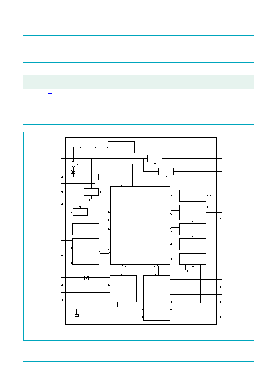
4.
Block diagram
Table 1.
Ordering information
Type number
Package
Name
Description
Version
UJA1061TW
[1]
HTSSOP32
plastic thermal enhanced thin shrink small outline package; 32 leads;
body width 6.1 mm; lead pitch 0.65 mm; exposed die pad
SOT549-1
Fig 1.
Block diagram
BAT42
BAT14
SYSINH
V3
INH/LIMP
INTN
TEST
SCK
SDI
SDO
SCS
RTLIN
LIN
TXDL
RXDL
GND
WAKE
32
27
29
30
17
7
16
11
9
10
12
26
25
3
5
23
18
V1
V2
RSTN
EN
RTH
CANH
CANL
TXDC
RXDC
4
20
6
8
24
RTL
19
21
22
13
14
SBC
FAIL-SAFE
SYSTEM
V1 MONITOR
RESET/EN
WATCHDOG
OSCILLATOR
GND SHIFT
DETECTOR
BAT
MONITOR
V1
V2
FAULT
TOLERANT
CAN
TRANSCEIVER
LIN
SPI
CHIP
TEMPERATURE
WAKE
INH
BAT42
BAT42
V2
001aad803
UJA1061
UJA1061_3
� Koninklijke Philips Electronics N.V. 2006. All rights reserved.
Preliminary data sheet
Rev. 03 -- 27 June 2006
5 of 67
Philips Semiconductors
UJA1061
Fault-tolerant CAN/LIN fail-safe system basis chip
5.
Pinning information
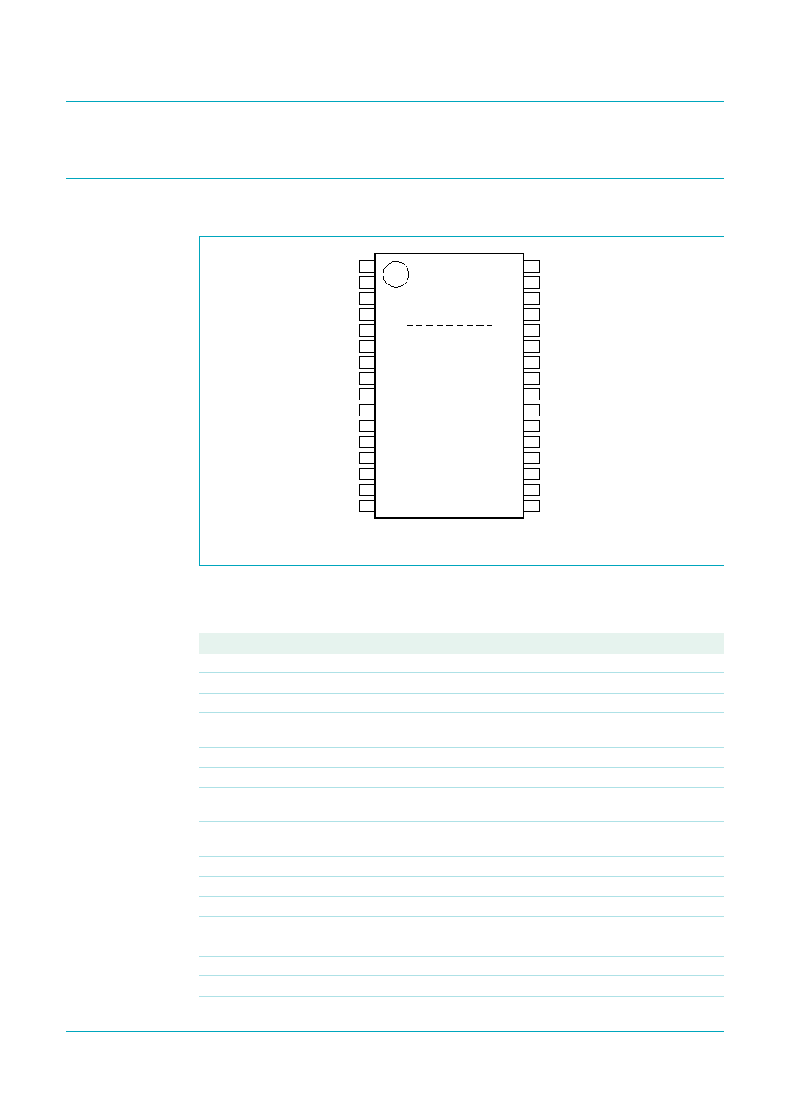
5.1 Pinning
5.2 Pin description
Fig 2.
Pin configuration
UJA1061
n.c.
BAT42
n.c.
RESERVED
TXDL
V3
V1
SYSINH
RXDL
n.c.
RSTN
BAT14
INTN
RTLIN
EN
LIN
SDI
RTH
SDO
GND
SCK
CANL
SCS
CANH
TXDC
V2
RXDC
RTL
n.c.
WAKE
TEST
INH/LIMP
001aad604
1
2
3
4
5
6
7
8
9
10
11
12
13
14
15
16
18
17
20
19
22
21
24
23
26
25
32
31
30
29
28
27
Table 2.
Pin description
Symbol
Pin
Description
n.c.
1
not connected
n.c.
2
not connected
TXDL
3
LIN transmit data input (LOW for dominant, HIGH for recessive)
V1
4
voltage regulator output for the microcontroller (3 V, 3.3 V or 5 V depending
on the SBC version)
RXDL
5
LIN receive data output (LOW when dominant, HIGH when recessive)
RSTN
6
reset output to microcontroller (active LOW; will detect clamping situations)
INTN
7
interrupt output to microcontroller (active LOW; open-drain, wire-AND this pin
to other ECU interrupt outputs)
EN
8
enable output (active HIGH; push-pull, LOW with every reset / watchdog
overflow)
SDI
9
SPI data input
SDO
10
SPI data output (floating when pin SCS is HIGH)
SCK
11
SPI clock input
SCS
12
SPI chip select input (active LOW)
TXDC
13
CAN transmit data input (LOW for dominant; HIGH for recessive)
RXDC
14
CAN receive data output (LOW when dominant; HIGH when recessive)
n.c.
15
not connected
TEST
16
test pin (should be connected to ground in application)