2003 Dec 12
2
Philips Semiconductors
Product specification
16-bit buffer/line driver, 30
series termination
resistors; 5 V tolerant input/output; 3-state
74LVC162244A;
74LVCH162244A
FEATURES
·
5 V tolerant inputs/outputs for interfacing with 5 V logic
·
Wide supply voltage range from 1.2 to 3.6 V
·
CMOS low power consumption
·
MULTIBYTE flow-through standard pin-out architecture
·
Low inductance multiple power and ground pins for
minimum noise and ground bounce
·
Direct interface with TTL levels
·
Inputs accept voltages up to 5.5 V
·
Integrated 30
termination resistors
·
All data inputs have bushold (74LVCH162244A only)
·
Complies with JEDEC standard no. 8-1A
·
ESD protection:
HBM EIA/JESD22-A114-A exceeds 2000 V
MM EIA/JESD22-A115-A exceeds 200 V.
·
Specified from
-
40 to +85
°
C and
-
40 to +125
°
C.
DESCRIPTION
The 74LVC(H)162244A is a high-performance, low power,
low voltage, Si-gate CMOS device, superior to most
advanced CMOS compatible TTL families. Inputs can be
driven from either 3.3 or 5 V devices. In 3-state operation,
outputs can handle 5 V. These features allow the use of
these devices as a mixed 3.3 and 5 V environment.
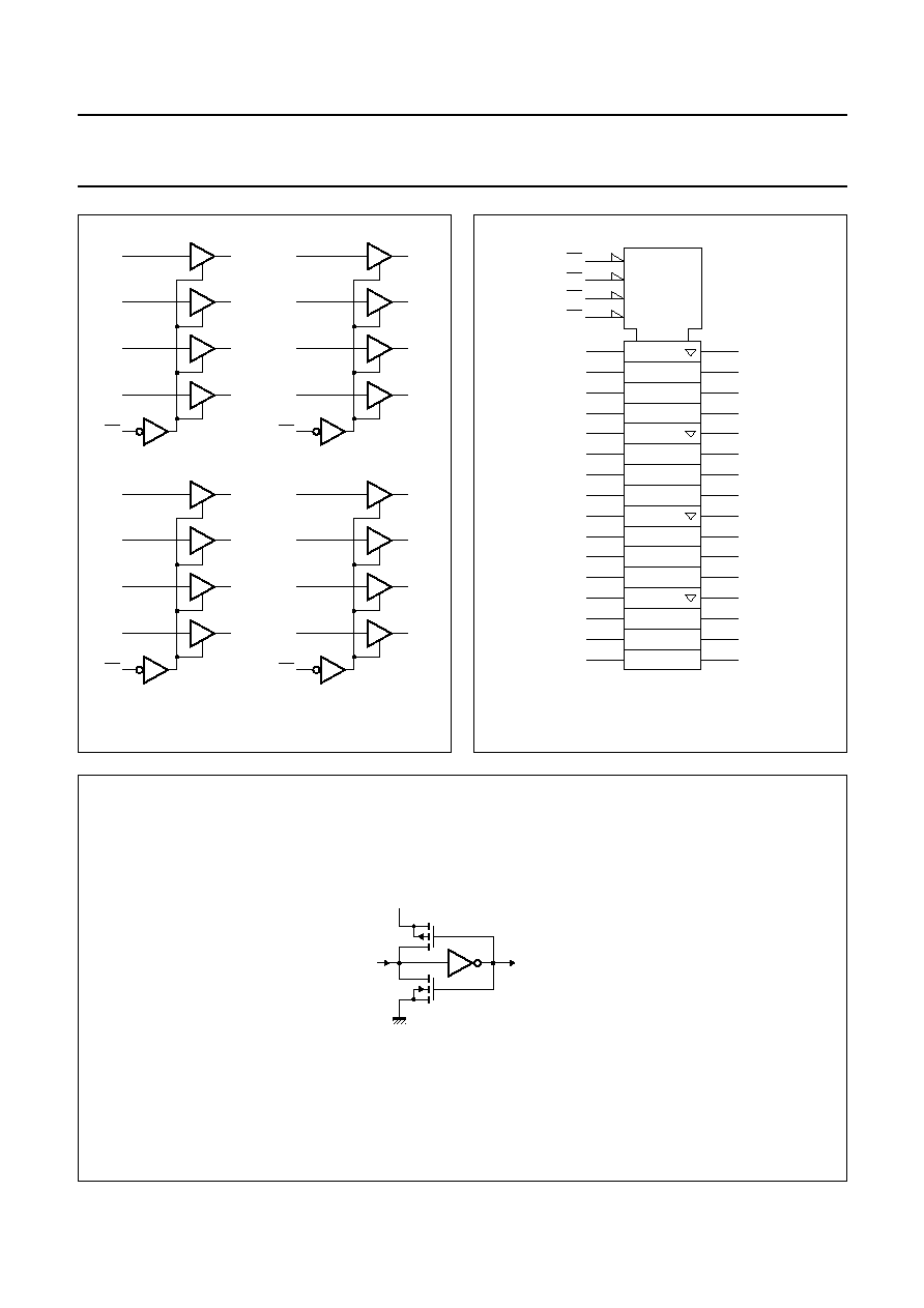
The 74LVC(H)162244A is a 16-bit non-inverting buffer/line
driver with 3-state outputs. The device can be used as four
4-bit buffers, two 8-bit buffers or one 16-bit buffer. The
3-state outputs are controlled by the output enable inputs
1OE, 2OE, 3OE and 4OE. A HIGH on nOE causes the
outputs to assume a high-impedance OFF-state.
The 74LVCH162244A bushold data inputs eliminates the
need for external termination resistors to hold unused
inputs.
The 74LVC(H)162244A is designed with 30
series
termination resistors in both HIGH and LOW output stages
to reduce line noise.
QUICK REFERENCE DATA
GND = 0 V; T
amb
= 25
°
C; t
r
= t
f
2.5 ns.
Notes
1. C
PD
is used to determine the dynamic power dissipation (P
D
in
µ
W).
P
D
= C
PD
×
V
CC
2
×
f
i
×
N +
(C
L
×
V
CC
2
×
f
o
) where:
f
i
= input frequency in MHz;
f
o
= output frequency in MHz;
C
L
= output load capacitance in pF;
V
CC
= supply voltage in Volts;
N = total load switching outputs;
(C
L
×
V
CC
2
×
f
o
) = sum of the outputs.
2. The condition is V
I
= GND to V
CC
.
SYMBOL
PARAMETER
CONDITIONS
TYPICAL
UNIT
t
PHL
/t
PLH
propagation delay nAn to nYn
C
L
= 50 pF; V
CC
= 3.3 V
3.0
ns
t
PZH
/t
PZL
3-state output enable time nOE to nYn
C
L
= 50 pF; V
CC
= 3.3 V
3.5
ns
t
PHZ
/t
PLZ
3-state output disable time nOE to nYn
C
L
= 50 pF; V
CC
= 3.3 V
2.8
ns
C
I
input capacitance
5.0
pF
C
PD
power dissipation capacitance per gate
V
CC
= 3.3 V; notes 1 and 2
outputs enabled
12
pF
outputs disabled
4.0
pF
2003 Dec 12
3
Philips Semiconductors
Product specification
16-bit buffer/line driver, 30
series termination
resistors; 5 V tolerant input/output; 3-state
74LVC162244A;
74LVCH162244A
ORDERING INFORMATION
FUNCTION TABLE
See note 1.
Note
1. H = HIGH voltage level;
L = LOW voltage level;
X = don't care;
Z = high-impedance OFF-state.
TYPE NUMBER
PACKAGE
TEMPERATURE
RANGE
PINS
PACKAGE MATERIAL
CODE
74LVC162244ADL
-
40 to +125
°
C
48
SSOP48
plastic
SOT370-1
74LVCH162244ADL
-
40 to +125
°
C
48
SSOP48
plastic
SOT370-1
74LVC162244ADGG
-
40 to +125
°
C
48
TSSOP48
plastic
SOT362-1
74LVCH162244ADGG
-
40 to +125
°
C
48
TSSOP48
plastic
SOT362-1
INPUT
OUTPUT
nOE
nAn
nYn
L
L
L
L
H
H
H
X
Z
2003 Dec 12
4
Philips Semiconductors
Product specification
16-bit buffer/line driver, 30
series termination
resistors; 5 V tolerant input/output; 3-state
74LVC162244A;
74LVCH162244A
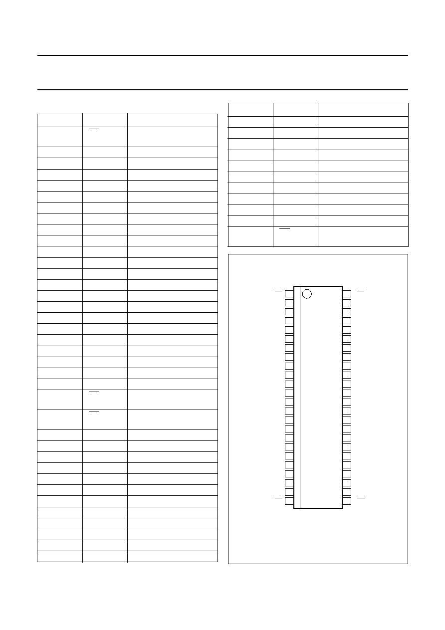
PINNING
PIN
SYMBOL
DESCRIPTION
1
1OE
output enable input
(active LOW)
2
1Y0
data output
3
1Y1
data output
4
GND
ground (0 V)
5
1Y2
data output
6
1Y3
data output
7
V
CC
supply voltage
8
2Y0
data output
9
2Y1
data output
10
GND
ground (0 V)
11
2Y2
data output
12
2Y3
data output
13
3Y0
data output
14
3Y1
data output
15
GND
ground (0 V)
16
3Y2
data output
17
3Y3
data output
18
V
CC
supply voltage
19
4Y0
data output
20
4Y1
data output
21
GND
ground (0 V)
22
4Y2
data output
23
4Y3
data output
24
4OE
output enable input
(active LOW)
25
3OE
output enable input
(active LOW)
26
4A3
data input
27
4A2
data input
28
GND
ground (0 V)
29
4A1
data input
30
4A0
data input
31
V
CC
supply voltage
32
3A3
data input
33
3A2
data input
34
GND
ground (0 V)
35
3A1
data input
36
3A0
data input
37
2A3
data input
38
2A2
data input
39
GND
ground (0 V)
40
2A1
data input
41
2A0
data input
42
V
CC
supply voltage
43
1A3
data input
44
1A2
data input
45
GND
ground (0 V)
46
1A1
data input
47
1A0
data input
48
2OE
output enable input
(active LOW)
PIN
SYMBOL
DESCRIPTION
162244A
001aaa252
1
2
3
4
5
6
7
8
9
10
11
12
13
14
15
16
17
18
19
20
21
22
23
24
48
47
46
45
44
43
42
41
40
39
38
37
36
35
34
33
32
31
30
29
28
27
26
25
1Y0
1Y1
GND
1A0
1A1
GND
1OE
2OE
1Y2
1Y3
V
CC
2Y0
2Y1
GND
2Y2
2Y3
3Y0
3Y1
GND
3Y2
3Y3
V
CC
4Y0
4Y1
GND
4Y2
4Y3
4OE
1A2
1A3
V
CC
2A0
2A1
GND
2A2
2A3
3A0
3A1
GND
3A2
3A3
V
CC
4A0
4A1
GND
4A2
4A3
3OE
Fig.1 Pin configuration.