 | –≠–ª–µ–∫—Ç—Ä–æ–Ω–Ω—ã–π –∫–æ–º–ø–æ–Ω–µ–Ω—Ç: VES1993 | –°–∫–∞—á–∞—Ç—å:  PDF PDF  ZIP ZIP |

comatlas S.A., 30 rue du ChÍne Germain, BP 814, 35518 CESSON-SEVIGNE Cedex, FRANCE
Phone : +33 (0)2 99 27 55 55, Fax : +33 (0)2 99 27 55 27, Internet : www.comatlas.fr / VES 1993 rev 2.0 / Jan 99
VES 1993
SINGLE CHIP
SATELLITE
CHANNEL RECEIVER
FEATURES
∑
DSS and DVB-S compatible single chip
demodulator & forward error correction.
∑
Dual 6-bit ADC on chip.
∑
PLL for crystal frequency multiplication.
∑
Variable rate BPSK/QPSK coherent
demodulator.
∑
Modulation rate from 1 to 45MBaud.
∑
Automatic Gain Control output.
∑
Digital symbol timing recovery :
Acquisition range up to
±
240ppm
∑
Digital carrier recovery :
Acquisition range up to
±
12% of symbol rate
∑
Half Nyquist baseband filters on chip
roll-off = 0.35 for DVB and 0.2 for DSS
∑
Channel quality estimation.
∑
Viterbi decoder :
Supported rates : from 1/2 to 8/9.
Constraint length K = 7
with G1 = 171
8
G2 = 133
8
VBER measurement provided.
∑
Convolutional deinterleaver and Reed
Solomon decoder according to DVB and
DSS specifications.
∑
Automatic Frame Synchronization.
∑
Selectable DVB-S descrambling.
∑
I2C bus interface.
∑
100-pin MQFP package.
∑
CMOS technology (0.35
µ
m 3.3V).
APPLICATIONS
∑
DSS receivers.
∑
DVB-S receivers (ETS 300-421).
∑
Direct Broadcast Satellite (DBS).
DESCRIPTION
The VES 1993 is a single-chip channel receiver for satellite television
reception which matches both DSS and DVB-S standards. The
device contains a dual 6-bit flash analog to digital converter, variable
rate BPSK/QPSK coherent demodulator and Forward Error
Correction functions.The ADCs directly interface with I and Q analog
baseband signals. After A to D conversion, the VES 1993 implements
a bank of cascadable filters as well as antialias and half-Nyquist
filters. Analog AGC signal is generated by an amplitude estimation
function. The VES 1993 performs clock recovery at twice the Baud
rate and achieves coherent demodulation without any feedback to
the local oscillator. Forward Error Correction is built around two error
correcting codes : a Reed-Solomon (outer code), and a Viterbi
decoder (inner code). The Reed-Solomon decoder corrects up to 8
erroneous bytes among the N bytes of one data packet.
Convolutional deinterleaver is located between the Viterbi output and
the R.S. decoder input. De-interleaver and R.S. decoder are
automatically synchronized thanks to the frame synchronisation
algorithm which uses the sync pattern present in each packet. The
VES 1993 is controlled via an I2C bus interface. The circuit operates
up to 91MHz and can process variable modulation rates, up to
45Mbaud.
The VES 1993 provides an interrupt line which can be programmed
on either events or timing information.
Designed in 0.35 CMOS technology and housed in a 100-MQFP
package, the VES 1993 operates over the commercial temperature
range.

comatlas reserves the right to make any change at anytime without notice.
VES 1993 rev 2.0 / Jan 99 / p2
CAUTION
This document is preliminary and is subject to change. Contact a comatlas,
representative to determine if this is the current information on this device.
The information contained in this document has been carefully checked and is believed to be reliable. However,
comatlas makes no guarantee or warranty concerning the accuracy of said information and shall not be responsible
for any loss or damage of whatever nature resulting from the use of, or reliance upon, it comatlas does not
guarantee that the use of any information contained herein will not infringe upon the patent, trademark, copyright,
mask work right or other rights of third parties, and no patent or other license is implied hereby.
This document does not in any way extend comatlas warranty on any product beyond that set forth in its standard
terms and conditions of sale. comatlas reserves the right to make changes in the products or specifications, or
both, presented in this publication at any time and without notice.
LIFE SUPPORT APPLICATIONS : comatlas products are not intended for use as critical components in life support
appliances, devices, or systems in which the failure of a comatlas product to perform could be expected to result in
personal injury.
comatlas reserves the right to do any kind of modifications in this datasheet regarding hardware or software
implementations without notice.
comatlas reserves the right to make any change at anytime without notice.
VES 1993 rev 2.0 / Jan 99 / p3
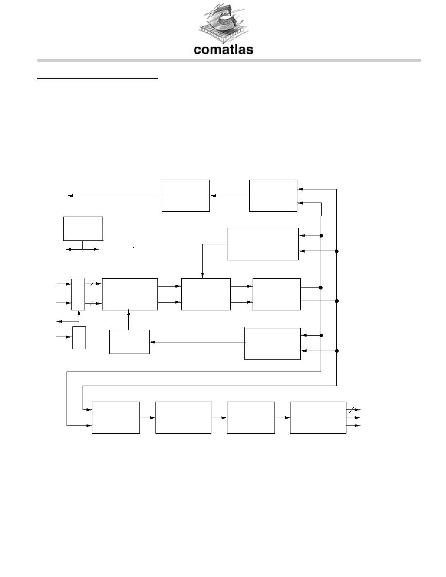
FIGURE 1. BLOCK DIAGRAM
1.1 WITH COMPLEX MULTIPLIER AFTER ANTI-ALIASING FILTERS (POSMUL=0) :
OCLK
DO
DEN
VAGC
DE-INTERLEAVER
DE-SCRAMBLER
DECODER
R - S
VITERBI
DECODER
DETECTION
AGC
ENCODER
PWM
.
CLOCK
SYNCHRONIZATION
MULTIPLIER
COMPLEX
NYQUIST
FILTERS
HALF
6
6
A D C
FILTER BANK
PLL
SACLK
XIN
VIN2
VIN1
CARRIER
SYNCHRONIZATION
NCO
INTERFACE
I2C
comatlas reserves the right to make any change at anytime without notice.
VES 1993 rev 2.0 / Jan 99 / p4
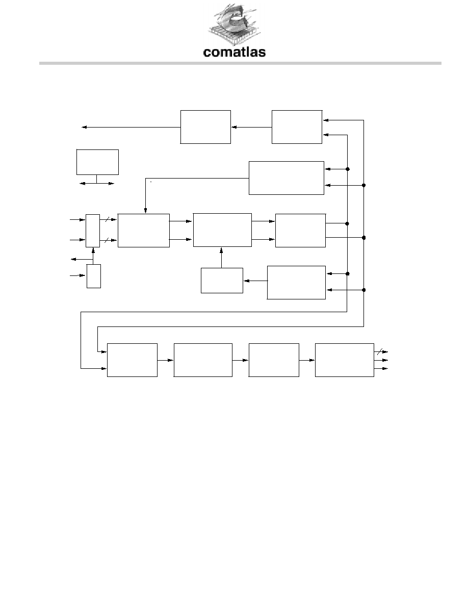
1.2 WITH COMPLEX MULTIPLIER BEFORE ANTI-ALIASING FILTERS (POSMUL=1) :
MULTIPLIER
COMPLEX
OCLK
DO
DEN
VAGC
DE-INTERLEAVER
DE-SCRAMBLER
DECODER
R - S
VITERBI
DECODER
DETECTION
AGC
ENCODER
PWM
.
CLOCK
SYNCHRONIZATION
NYQUIST
FILTERS
HALF
6
6
A D C
PLL
SACLK
XIN
VIN2
VIN1
CARRIER
SYNCHRONIZATION
INTERFACE
I2C
FILTER BANK
NCO

comatlas reserves the right to make any change at anytime without notice.
VES 1993 rev 2.0 / Jan 99 / p5
TABLE 1 : ABSOLUTE MAXIMUM RATINGS
Parameter
Min
Max
Unit
Ambient operating temperature (Ta)
0
70
∞C
DC supply voltage
- 0.5
+4.1
V
DC input voltage
- 0.5
VDD + 0.5
V
DC input current
±
20
mA
Lead Temperature
+ 300
∞C
Junction Temperature
+ 125
∞C
Stresses above the absolute maximum ratings may cause permanent damage to the device. Exposure to absolute
maximum ratings conditions for extended periods may affect device reliability.
TABLE 2: RECOMMENDED OPERATING CONDITIONS
Symbol
Parameter
Min
Typ
Max
Unit
Notes
VDD
Digital supply voltage
3.135
3.3
3.465
V
3.3V ±5%
VCC
5V supply voltage
4.75
5
5.25
V
pins 22 and 91
Ta
Operating temperature
0
70
∞ C
Ambient temperature
AVD
Analog supply voltage
3.135
3.3
3.465
V
pin 43
AVS
Analog ground
0
V
pin 44
VINDC
DC Analog Input
VREFN
VREFP
V
pins 41 and 45
VINAC
AC Analog Input
750
mVpp
pins 41 and 45
ZIN
Analog input impedance
10
100
Ohms
pins 41 and 45
VREFP
Top voltage reference
2.0
V
pin 46
VREFN
Bottom voltage reference
1.25
V
pin 42
XIN
Crystal frequency
93
MHz
ZOE (1)
Zero Offset Error
10
mV
DNL(2)
Differential Non Linearity
0.5
0.9
LSB
INL(3)
Integral Non Linearity
0.8
1
LSB
GE (4)
Gain Error
10
mV
SINAD (5)
ADC signal to noise ratio
34
dB
@ 1MHz input signal
and 92MHz sampling clock
THD(6)
Total Harmonic Distorsion
35
dB
VIH(7)
High-level input voltage
2
VCC+0.3
V
TTL input
VIL
Low-level input voltage
-0.5
0.8
V
TTL input
VOH(8)
High-level output voltage
2.4
V
@IOH = -2mA to -4mA
VOL(8)
Low-level output voltage
0.4
V
@IOL = + 2 mA to +4mA
IDD
Supply current
8.5
mA/MBaud
@XIN = 91MHz
CIN
Input capacitance
15
pF
1MHz input to VSS
COUT
Output capacitance
15
pF
1MHz input to VSS
(1) Zero Offset Error : deviation of voltage input from ideal voltage to get the 00 code.
(2) Differential Non linearity : maximum deviation of the analog span of each output code from its ideal 1lsb value.
(3) Integral Non linearity : deviation of the ADC transfer curve from the ideal transfer curve, defined according to the
best straight line fit method.
(4) Gain Error : Deviation of voltage input from ideal value to get the highest code.
(5) Signal-to-noise plus distortion ratio (SINAD) : ratio between the RMS magnitude of the fundamental input
frequency to the RMS magnitude of all other A/D output signals.
(6) Total harmonic distortion (THD) : ratio of the RMS sum of all harmonics of the input signal (below one half of the
sample rate) to the fundamental.
(7) All inputs are 5V tolerant.
(8) IOH, IOL = ±4mA only for pins : SACLK, OCLK, SDA, SCL_0, SDA_0.