W i r e l e s s C o m m u n i c a t i o n s
OVERVIEW
The VWS26001 is a highly-integrated
Bluetooth baseband processor designed
to form the heart of standalone and
embedded Bluetooth wire l e s s
communication systems.
Bluetooth is a low-cost cable re p l a c e m e n t
technology using short-range wire l e s s
links to provide "ad hoc" networking
between portable devices. Bluetooth
p rovides ubiquitous communication
capabilities for a range of consumer
e l e c t ronics devices ranging from
cell phones, PDAs and computers
to digital cameras and fax machines.
The five founding members of the
Bluetooth consortium (Ericsson, IBM,
Intel, Nokia and Toshiba) have since
been joined by over 500 companies, thus
setting the standard for worldwide
success and rapid market gro w t h .
Bluetooth technology offers the
following benefits:
· Open standard
· Both voice and data support
· Usable worldwide
· "Ad hoc" operation simplifies network
s e t u p
· Designed to withstand interf e rence in
unlicensed bands
· Can be implemented in very small
modules, saving space in end equipment
· Ve ry low power consumption
· Designed to reduce system bill-of-
materials costs
The VWS26001 Bluetooth Pro c e s s o r,
first member of the VWS26000 Bluetooth
f a m i l y, was developed by VLSI to an
Ericsson specification, thus minimizing
risk and ensuring compliance and inter-
operability with the Bluetooth standard.
The integrated enhanced ARM7TDMI
microprocessor runs the complete
VWS26001 BLUETOOTH
BASEBAND PROCESSOR
Bluetooth protocol stack while the on-chip
peripherals pro v i d e for easy interf a c i n g
to a Bluetooth radio module and to a
host system.
FEATURES
· Integrated ARM7TDMI
m i c ro c o n t ro l l e r
· Bluetooth core encapsulating Ericsson
IP (EBC)
· Ericsson Protocol stack executes
o n - c h i p
· On-chip UART, as well as USB, PCM
and I
2
C
TM
i n t e rf a c e s
· Implemented in 0.25 um CMOS
t e c h n o l o g y
· Packaged in 96-pin FPBGA package
for small footprint
· Utilizes Received Signal Stre n g t h
Indication (RSSI) for adaptive
transmit power contro l
P o w e r ful single-chip ar c h i t e c t u r e for
Bluetooth-enabled applications
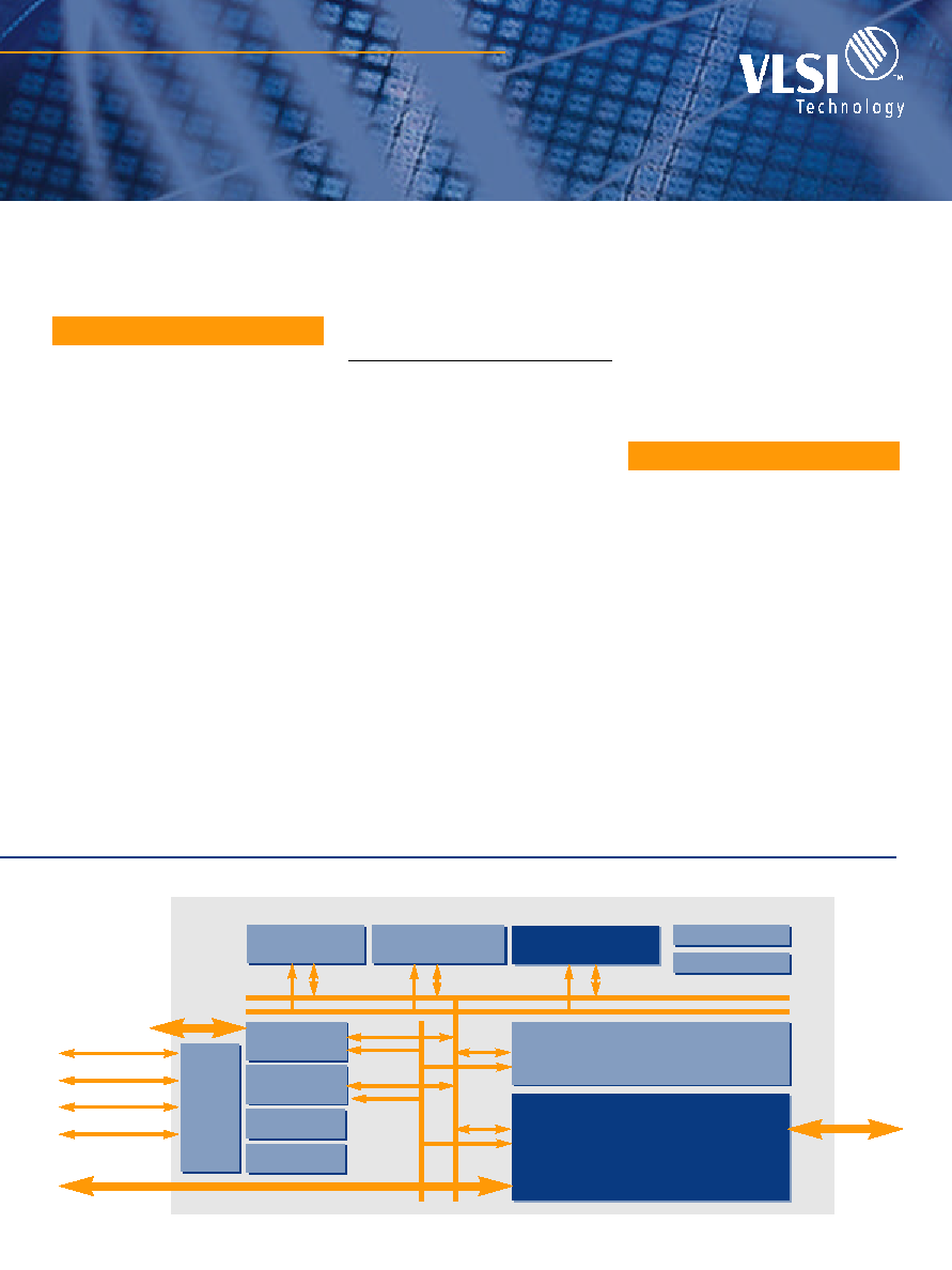
V W S 2 6 0 0 1 B a s e b a n d P r o c e s s o r B l o c k D i a g r a m
Counters/Timers
External Bus
Control
SDRAM
EBC
UART 1,2,3
FIFOs
I/O
Mode
Select
I
2
C
USB
Inter rupt Controllers
ARM Core
Clock Control
IROM
Counters/Timers
External Bus
Control
SDRAM
EBC
UART 1,2,3
FIFOs
I/O
Mode
Select
I
2
C
USB
Interrupt Controllers
ARM Core
Clock Control
Radio
Interface
Baseband
PCM CLK
DATA IN/OUT
USB+ USB-
IROM
I
2
C
UART2
UART3/I
2
C
HDLi and Velocity are trademarks of VLSI Te c h n o l o g y, Inc. Bluetooth and the Bluetooth logo are trademarks of the Bluetooth
Special Interest Group. Other trademarks and re g i s t e red trademarks are pro p e rty of their respective owners.
VLSI Te c h n o l o g y, Inc.
1109 McKay Drive
San Jose, CA 95131
U S A
With respect to the information in this document, VLSI
Technology, Inc. (VLSI) makes no guarantee or warranty of its
accuracy or that the use of such information will not infringe
upon the intellectual rights of third parties. VLSI shall not be
responsible for any loss or damage of whatever nature resulting
from the use of, or reliance upon it and no patent or other
license is implied hereby. This document does not in any way
extend or modify VLSI's warranty on any product beyond that set
forth in its standard terms and conditions of sale. VLSI reserves
the right to make changes in its products and specifications at
any time and without notice.
LIFE SUPPORT APPLICATIONS:
V L S I 's products are not intended for use as critical com-
ponents in life support appliances, devices, or systems, in
which the failure of a VLSI product to perf o rm could be
expected to result in personal injury.
For update information, please visit our website a t
h t t p : / / w w w.vlsi.com
or call the Worldwide Headquarters at
+ 1 - 4 0 8 - 4 3 4 - 3 1 0 0
or the European Headquarters at +49/89/627 06-0
or E-mail us at bluetooth@vlsi.com
© 1999 VLSI Technology, Inc. Printed in USA. Document Control: BlueTooth BBP V1.0 March 99
V W S 2 6 0 0 1 B l u e t o o t h P r o c e s s o r
· Supports key Bluetooth features such as:
· Fast frequency hopping
· CVSD (Continuously Variable Slope
Delta-modulation) speech coding
· Advanced security functions
LOW RISK
The VWS26001 is directly compatible
with the Ericsson-developed Bluetooth
radio module, thus re d u c i n g
development time and risk.
LOW POWER
The VWS26001 device makes use of
VLSI's low-power design expertise and is
implemented in VLSI's leading-edge
0.25 um CMOS technology to deliver
minimal power consumption with
c o rrespondingly longer battery lifetimes.
The VWS26001 also allows adaptive
radio transmit power control based on
RSSI measurement, providing scope for
f u rther dynamic reduction of system
power consumption.
BLUETOOTH MODULE
The first generation of Bluetooth-
enabled products will make use of
Bluetooth `modules' which include both
radio and baseband functionality. VLSI's
VWS26001 processor is at the heart of a
number of Bluetooth modules curre n t l y
under development by OEMs.
Radio
· Operates in 2.4GHz ISM band
( u n l i c e n s e d )
· F requency hopping, spread spectru m
t e c h n o l o g y
· Up to 79 "hop" channels
· 1MHz bandwidth per channel
· Peak data rate 1Mb/s
· S t a n d a rd range <10m (0dBm),
<100m option (+20dBm)
Protocol Stack
· Link Manager (LM)
· Logical Link Control + Adaptation
P rotocol (L2CAP)
· Host Controller Interface (HCI)
Baseband
· F requency "hop" selection
· Tr a n s m i t / receive timing
· Radio interf a c e
· FEC, CRC, ARQ
· PCM conversion
· E n c ryption and authentication
AVAILABILITY
The VWS26001 baseband processor is
now sampling and will be available in
p re - p roduction quantities in mid-1999.
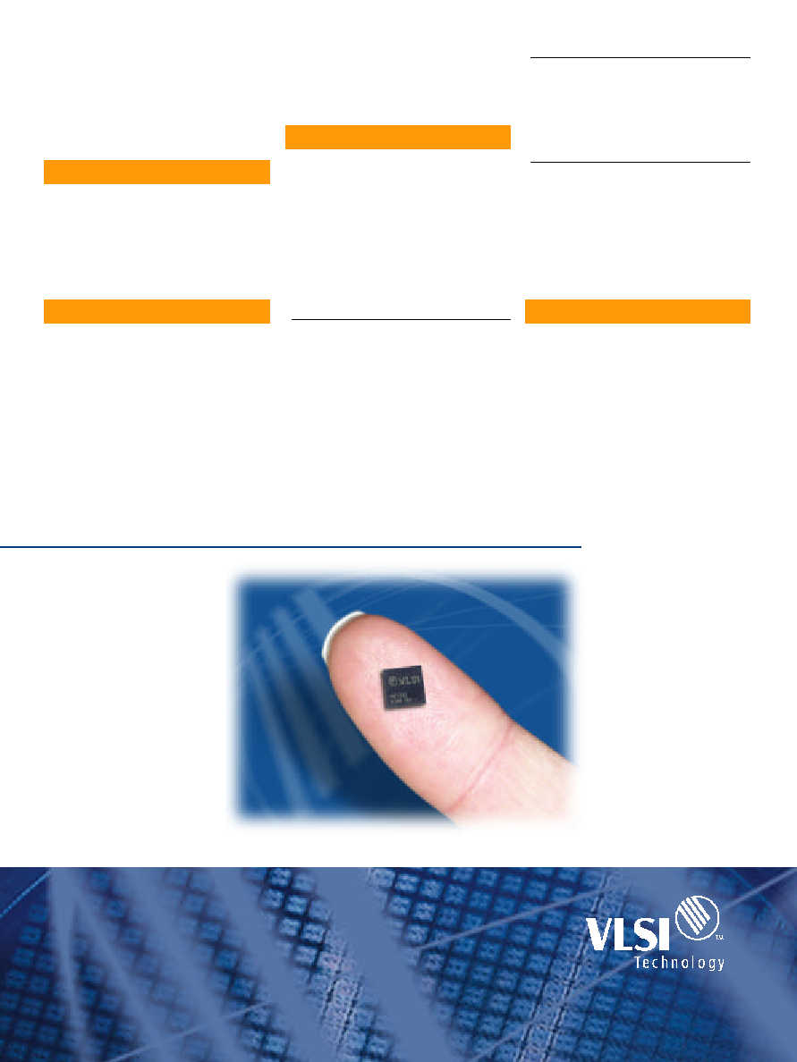
Implemented in an
8x8mm 96 FPBGA pack-
age, the highly
integrated Bluetooth
Baseband Pro c e s s o r
optimizes both size
and cost while
delivering minimal
power consumption.