
SD112-45-11-221
Si Photodetector with High Gain Amplifier
The SD112-45-11-221 features an ultra low dark current photodiode
integrated with a high gain transimpedance amplifier in a hermetic TO-5
package. The amplifier has a typical input bias current of 10 fA resulting in
very low output offset voltage and drift. The hermetic package helps keep the
device's performance stable over wide range of environmental conditions.
Because of excellent parameters the SD112-45-11-221 can often replace costly
cooled detectors. The device can be also customized with even higher
transimpedance gain.
The SD112-45-11-221 can be used in any application that requires precise
very low light level detection within limited bandwidth.
Electro-Optical Characteristics
@ +23∞C, V
S
=
±5V, R
L
>1M
, unless otherwise specified
Parameter
Conditions
Min
Typ
Max
Units
Active Area
5.55
mm
2
Transimpedance Gain
600
M
Offset Voltage
0.08
1
mV
Sensitivity
= 633 nm
2.0 x 10
8
2.4 x 10
8
V/W
Spectral Range
350
1100
nm
Broadband Output Noise
0.01 Hz to 135 Hz
52
µV
NEP
0.01 Hz to 135 Hz
30
fW/
Hz
Bandwidth
110
135
Hz
Supply Current
850
950
µA
Output Voltage Swing
0 to 4.7
0 to 4.8
V
ABSOLUTE MAXIMUM RATINGS*
Supply Voltage (V
+
- V
-
) 16V
Operating Temperature
-40
∞C + 85∞C
Storage Temperature
-55
∞C + 100∞C
Lead Solder Temperature
260
∞C (soldering, 10 sec.)
*Operating beyond these limits may cause permanent damage to the device.
Features
∑ Large active area
∑ High sensitivity
∑ Low noise
∑ Low output offset
∑ Hermetically sealed
Applications
∑ Analytical Instrumentation
API reserves the right to change specifications without notification.
Rev. October 30, 2001
Preliminary
All dimensions in inches
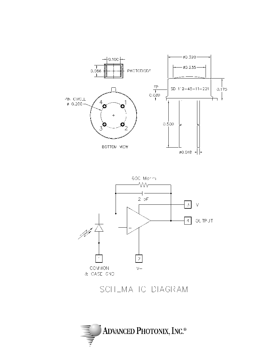
MECHANICAL DIMENSIONS, PIN-OUT AND SCHEMATIC
1240 Avenida Acaso, Camarillo, CA 93012
(805) 987-0146 Fax (805) 484-9935
www.advancedphotonix.com