PJ2108
Dual Differential Input Operational Amplifiers
And Voltage Reference
1-3
2002/01.rev.A
he PJ2108 is a monolithic IC that includes one
independent op-amp and another op-amp for which the
non inverting input is wired to a 2.5V fixed Voltage
Reference. This device is offering space and cost saving in
many applications like power supply management or data
acquisition systems
OPERATIONA AMPLIFIER
∑ Low input offset voltage : 0.5mV typ. For PJ2108
∑ Low supply current : 350
µA/op. (@ V
CC
=5V)
∑ Medium bandwidth (unity gain) : 0.9MHz
∑ Large output voltage swing : 0V to (Vcc-1.5V)
∑ Input common mode voltage range includes ground
∑ Wide power supplu range : 3 to 32V ,
±1.5 to ±16
VOLTAGE REFERENCE
∑ Fixed output voltage reference 2.5V
∑ 0.4% and 1% voltage precision
∑ Sink current capability : 1 to 100mA
∑ Typical output impedance : 0.2
T
Device
Operating Temperature
(Ambient)
Package
PJ2108CD
DIP-8
PJ2108CS
-20 to +85
SOP-8
FEATURES
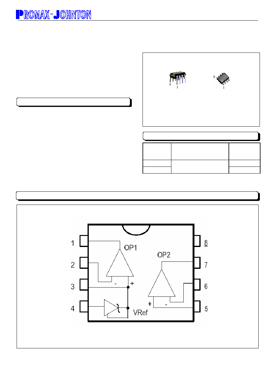
Pin : 1. Output A 5. Non-Inverting Input B
2. Inverting Input A 6. Inverting Input B
3. Non-Inverting Input A 7. Output B
4. Vcc - 8. V
CC
+
ORDERING INFORMATION
BLOCK DIAGRAM
DIP-8
SOP-8

PJ2108
Dual Differential Input Operational Amplifiers
And Voltage Reference
2-3
2002/01.rev.A
TOTAL SUPPLY VOLTAGE SECTION
Characteristics Symbol
Conditions Min
Typ
Max
Unit
Total Supply Current
Vcc=0V, No Load
Operational Amplifiers
Input Offset Voltage
Vio
--
1
4.5
mA
Input Bias Current
Iib
--
50
150
nA
Input Common-Mode Voltage Range
Vicm
V
CC
= 30 V
V
CC
= 30 V , (T
A
=85 to -10
)
0.4 --
Voc-
1.2V
V
Slew Rate
SR Vi=10V,
Vcc=12V
Rload=10K, Cload=100pF
-- 0.75 -- V/
µs
Large Signal Voltage Gain
Avd
R
L
= 2.0K , V
CC
=15V,
For Large V
O
Swing,
T
A
=85
to -20
60
100
--
dB
Common Mode Rejection Ratio
CMRR
Vcc=15V
70
90
--
dB
Power Supply Rejection Ratio
SVRR
Vcc=5V to 15V
65
100
--
dB
Output Source Current
Isource
Vo=2.5V, Vid=+1V
3
6
--
mA
Output Voltage -- High
Voh
Vcc=15V, Rload=10K
12
13
--
V
Output Voltage -- Low
Vol
Rload=10K
--
100
250
mV
Gain Bandwidth
GB
Rload=10K,
Cload=100pF,f=100KHz
-- 1.5 -- MHz
Phase Margin
PM
Rload=10K, Cload=100pF
--
55
55
Degree
Total Harmonic Distortion
THD
--
0.05
--
%
Output Sink Current
Isink V0=2.5V,
Vid=-1V
3 6 --
mA
ADJUSTABLE SHUNT REGULATOR
Characteristics Symbol
Conditions Min
Typ
Max
Unit
Recommended Cathod Current
Ik
0.5
--
100
mA
Reference Input Voltage
Vref
PJ2108
2.475
2.5
2.525
V
Reference Input Voltage Deviation
dVref
Vka=Vref, Ik=10mA
-40< Ta < 105
-- 7 30
mV
Load Regulation
Rload
Ik=1mA ≠ 10mA
--
3
10
mV
MinimumCathod Current for
Regulation
Imin
-- 0.2 0.5 mA
Rating Symbol
PJ358
Unit
Power Supply Voltage Single Supply
Split Supplies
V
CC
V
CC
, V
EE
32
±16
Vdc
Input Differential Voltage Range (1)
V
IDR
±32 Vdc
Input Common Mode Voltage Range (2)
V
ICR
-0.3 to 32
Vdc
Input forward current (3) (VI --0.3V)
I
IF
50
mA
Output Short Circuit Duration
t
S
Continuous
Junction Temperature Plastic Packages
T
J
150
Storage Temperature Range Plastic Packages
T
stg
-55 to +125
ABSOLUTE MAXIMUM RATINGS
ELECTRICAL CHARACTERISTICS
(T
A
=25, Vcc = 5V unless otherwlse noted).
ELECTRICAL CHARACTERISTICS
(T
A
=25, Vcc = 5V unless otherwlse noted).
PJ2108
Dual Differential Input Operational Amplifiers
And Voltage Reference
3-3
2002/01.rev.A
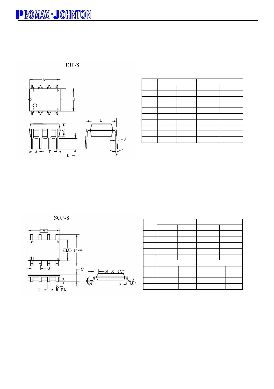
MILLIMETERS
INCHES
DIM MIN MAX MIN MAX
A 9.07 9.32 0.357 0.367
B 6.22 6.48 0.245 0.255
C 3.18 4.43 0.125 0.135
D 0.35 0.55 0.019 0.020
G 2.54BSC
0.10BSC
J 0.29 0.31 0.011 0.012
K 3.25 3.35 0.128 0.132
L 7.75 8.00 0.305 0.315
M - 10∞
-
10∞
MILLIMETERS
INCHES
DIM
MIN MAX
MIN MAX
A 4.80 5.00 0.189 0.196
B 3.80 4.00 0.150 0.157
C 1.35 1.75 0.054 0.068
D 0.35 0.49 0.014 0.019
F 0.40 1.25 0.016 0.049
G 1.27BSC
0.05BSC
K 0.10 0.25 0.004 0.009
M 0∞ 7∞
0∞ 7∞
P 5.80 6.20 0.229 0.244
R 0.25 0.50 0.010 0.019