 | –≠–ª–µ–∫—Ç—Ä–æ–Ω–Ω—ã–π –∫–æ–º–ø–æ–Ω–µ–Ω—Ç: PJ324CS | –°–∫–∞—á–∞—Ç—å:  PDF PDF  ZIP ZIP |
PJ324
Quad Low Power Operational Amplifiers
1-7
2002/01 VER.A
he PJ324 series are low-cost , quad operational amplifiers
with true differential inputs. These have several distinct
advantage over standard operational amplifier types in single
supply applications. The quad amplifiers can operate at supply
voltages as low as 3.0V or as high as 32V with very low
quiescent currents and eliminat the necessity for external
biasing components in many
applications. The output voltage range also includes the
negative power supply voltage.
∑ Short circuited protected outputs
∑ True differential input stage
∑ Single supply operation:3.0V to 32V
∑ Low input bias currents:100nA Max
∑ Four amplifiers per package
∑ Internally compensated
∑ Common mode range extends to negative supply
∑ Industry standard pinouts
∑ ESD clamps on the inputs increase raggedness without
affecting device operation
Device Operating
Temperature
Package
PJ324CD DIP-14
PJ324CS
-20 to +85
SOP-14
Rating Symbol
PJ324
Unit
Power Supply Voltage
Single Supply
Split Supplies
V
CC
V
CC,
V
EE
±16 Vdc
Input Differential Voltage
Range (1)
V
IDR
32
Vdc
Input Common Mode Voltage
Range
V
ICR
-0.3 to 32
Vdc
Output Short Circuit Duration
t
SC
Continuous
Junction Temperature
Plastic Packages
T
J
150
Storage Temperature
Ceramic Package
Plastic Packages
T
stg
- 65 to + 150
NOTE : 1. Split Power Supplies.
T
FEATURES
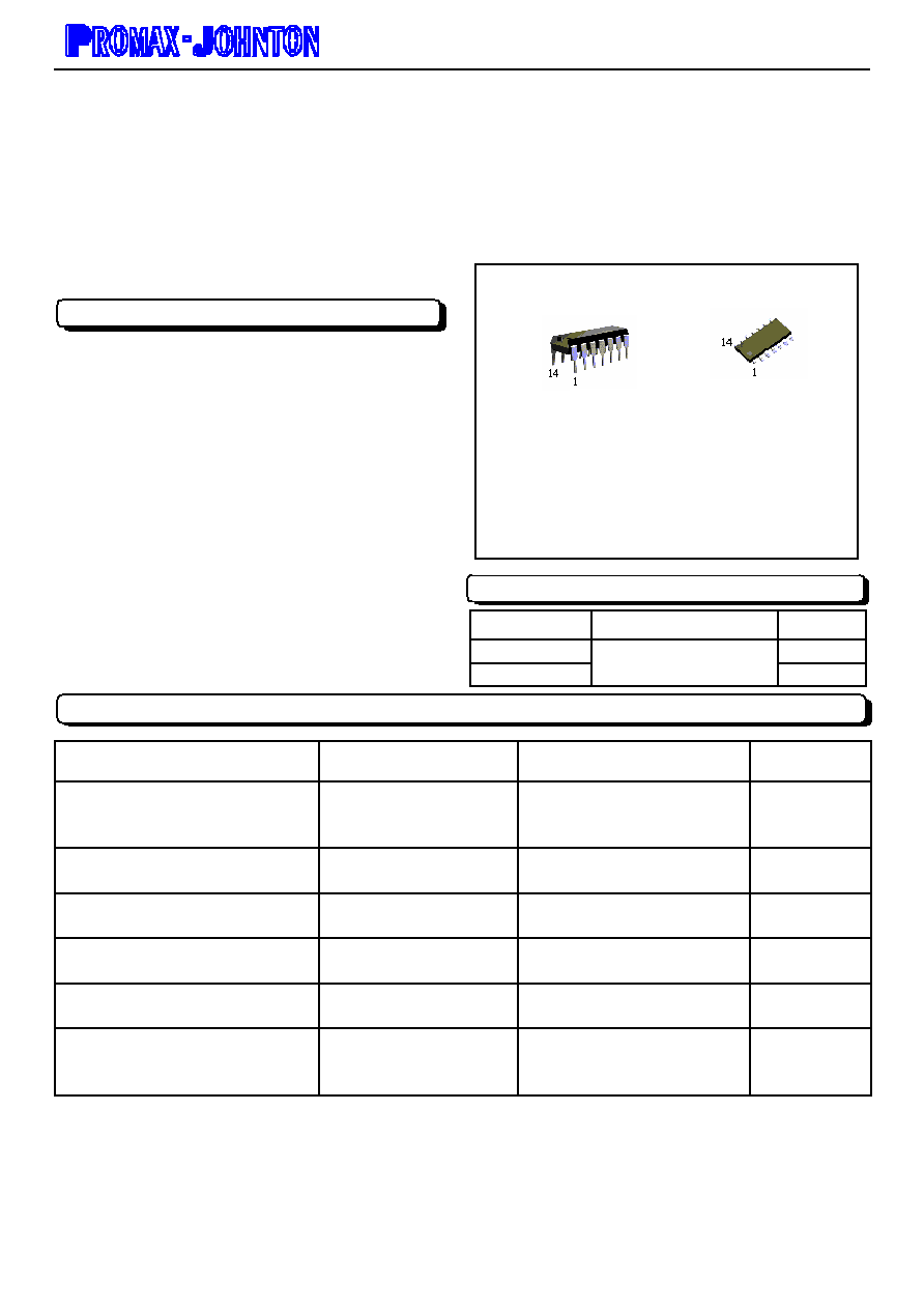
DIP-14
SOP-14
ORDERING INFORMATION
MAXIMUM RATING
(Ta=+25,unless otherwise noted.)
Pin:
1.Output 1 8.Output 3
2.Input 1 (-) 9.Input 3 (-)
3.Input 1(+) 10.Input 3 (+)
4.Vcc 11.Vee Gnd
5.Input 2(+) 12.Input 4 (+)
6.Input 2 (-) 13.Input 4 (-)
7.Output 2 14.Output 4

PJ324
Quad Low Power Operational Amplifiers
2-7
2002/01 VER.A
PJ324
Characteristics Symbol
Min
Typ
Max
Unit
Input Offset Voltage
V
CC
=5.0V to 30V
V
ICR
=0 V to V
CC
-0.7V, Vo=1.4V, Rs=0
T
A
=25
T
A
=T
high
to T
low
(Note 1)
V
IO
-
-
2.0
-
7.0
9.0
mV
Average Temperature Coefficient of Input Offset Voltage
T
A
=T
hige
to T
low
(Note 1)
V
IO
/T
-
7.0
-
V/
Input Offset Current
T
A
=T
hige
to T
low
(Note 1)
I
IO
-
-
5.0
-
50
150
nA
Average Temperature Coefficient of Input Offset Current
T
A
=T
hige
to T
low
(Note 1)
I
IO
/T
-
10
-
pA/
Input Bias Current
T
A
=T
hige
to T
low
(Note 1)
I
IB
-
-
-90
-
-250
-500
nA
Input Common Mode Voltage Range (Note 2)
V
CC
=30V
V
CC
=30V, T
A
=T
hige
to T
low
V
ICR
0
0
-
-
28.3
28
V
Differential Input Voltage Range
V
IDR
- - V
CC
V
Large Signal Open-Loop Voltage Gain
R
L
=2.0K, V
CC
=15V, for Large Vo Swing
T
A
=T
hige
to T
low
(Note 1)
A
VOL
25
15
100
-
-
-
V/mV
Channel Separation
10KHzf20KHz, Input Referenced
CS
- -120 - dB
Common Mode Rejection
Rs10K
CMR 65 70
-
dB
Power Supply Rejection
PSR
65
100
-
dB
Output Voltage - High Limit ( T
A
=T
hige
to T
low
)
(Note 1)
V
CC
=5.0V, R
L
=10K,T
A
=25
V
CC
=30V, R
L
=2.0K
V
CC
=30V, R
L
=10K
V
OH
3.3
26
27
3.5
-
28
-
-
-
V
Output Voltage-Low Limit
V
CC
=5.0V, R
L
=10K, T
A
=T
hige
to T
low
(Note 1)
V
OL
-
5.0
20
mV
Output Source Current (V
ID
=+1.0V, V
CC
=15V)
T
A
=25
T
A
=T
hige
to T
low
(Note 1)
I
O
+
20
10
40
20
-
-
mA
Output Sink Current
(V
ID
= -1.0V, V
CC
=15V)
T
A
=25
T
A
=T
hige
to T
low
(Note 1)
(V
ID
= -1.0V, V
CC
=200mV, T
A
=25)
Io
-
10
5.0
12
20
8.0
50
-
-
-
mA
A
Output Short Circuit Ground (Note 2)
Isc
-
40 60
mA
Power Supply Current (T
A
=T
hige
to T
low
)
(Note 1)
V
CC
=30V (26V for LM2902), Vo=0V, R
L
=
V
CC
=5.0V, Vo=0V, R
L
=
Icc
-
-
-
-
3.0
1.2
mA
Note: 1. Short circuits from the output to Vcc can cause excessive heating and eventual destruction . Destructive dissipation can
result from simultaneous shorts on all amplifiers.
2. The input common mode voltage or either input signal voltage should not be allowed to go negative by more than
0.3V The upper end of the common mode voltage range is Vcc-1.7V.
ELECTRICAL CHARACTERISTICS (V
CC
= 5.0V, V
EE
=GND, T
A
= 25
unless otherwise noted.)
PJ324
Quad Low Power Operational Amplifiers
3-7
2002/01 VER.A
µ
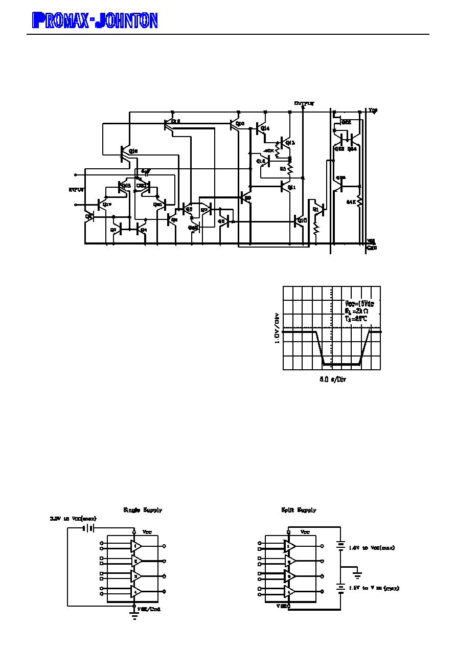
Representative Circuit Schematic
(O ne-Fourth of Circuit Shown)
CIRCUIT DESCRIPTION
T he PJ324 series is made using four internally
compensated, two-stage operational amplifiers. T he
first stage of each consists of differential input
devices Q20 and Q18 with input buffer transistors
Q21 and Q17 and the differential to single ended
converter Q3 and Q4 . T he first stage performs not
only the first stage gain function but also performs
the level shifting and transconductance reduction
functions. By reducing the transconductance a smaller
compensation capacitor (only 5.0pF ) can be
employed , thus saving chip area. T he
transconductance reduction is accomplished by
splitting the collectors of Q20 and Q18 . Another
feature of this input stage is that the input common
mode range can include the negative supply or ground,
in single supply operation without saturating either
the input devices or the differential to single-ended
converter . T he second stage consists of a standed
current source load amplifier stage.
Large Signal Voltage Follower Response
Each amplifier is biased from an internal voltage
regulator which has a low temperature coefficient thus
giving each amplifier good temperature characteristics
as will as excellent power supply rejection.

PJ324
Quad Low Power Operational Amplifiers
4-7
2002/01 VER.A
Figure 1.Input Voltage Range
Figure 3.Large-Signal Frequency Response
Figure 5.Power Supply Current versus
Power Supply Voltage
Figure 2.Open-Loop Frequency
Figure 4.Small-Signal Voltage Follower
Pulse Response (Noninverting)
Figure 6.Input Bias Current versus
Power Supply Voltage

PJ324
Quad Low Power Operational Amplifiers
5-7
2002/01 VER.A
Figure 7.Voltage Reference
Vo = 2.5V (1+ R1/ R2)
Figure 9.High Impedance Differential Amplifier
e
o
=C (1+a+b) (e2- e1)
Figure 8.Wlen Bridge Oscillator
fo = 1/2RC
For: fo =1.0KHz
R=16K
C =0.01F
Figure 10.Comparator with Hysteresis
V
inL
= R1/R1 + R2 (V
OL
-V
ref
) +V
ref
V
inH
= R1 /R1 + R2 (V
OH
-V
ref
) +V
ref
H = R1/R1 + R2 (V
OH
-V
OL
)
fo = 1/2RC
R1 = OR
R2 = R1/ T
BP
V
ref
= 1/2
R3 =T
NR2
C1 =10C
For : fo =1.0 Khz
Q =10
T
BP
=1
T
N
=1
R =160 K
C =0.001F
R1 =1.6M
R2 =1.6M
R3 =1.6M
Figure 11.Bi-Q uad Filter
Where : T
BP
=Center Frequency
Gain
T
N
= Passband Notch Gain
PJ324
PJ324
PJ324
PJ324
PJ324
PJ324
PJ324