 | –≠–ª–µ–∫—Ç—Ä–æ–Ω–Ω—ã–π –∫–æ–º–ø–æ–Ω–µ–Ω—Ç: PJ78M18CZ | –°–∫–∞—á–∞—Ç—å:  PDF PDF  ZIP ZIP |
PJ78M00 Series
3-Terminal Medium Current Positive Voltage Regulators
1-10 2001/10.rev.
A
he PJ78M00Series positive voltage regulators are
identical to the popular PJ7800Series devices, except that
they are specified for only half the output current. Like thhe
PJ7800 devices, the PJ78Mxx Terminal regulators are
intended for local,ocard voltage regulation.
Internal current limiting,thermal shutdown circuitry and safe-
area compensation for the internal pass transistor combine to
make these devices remarkably rugged under most operating
conditions.Maximum output current, with adequate heatsinking
is 500mA
No External Components Required
Internal Thermal Overload Protection
Internal Short Circuit Current
Limiting
Output Transistor Safe-Area
Compensation
T
Device Operating
Temperature
Package
PJ78MxxC
Z
TO-220
PJ78MxxCP
-20 ~ +85
TO-252
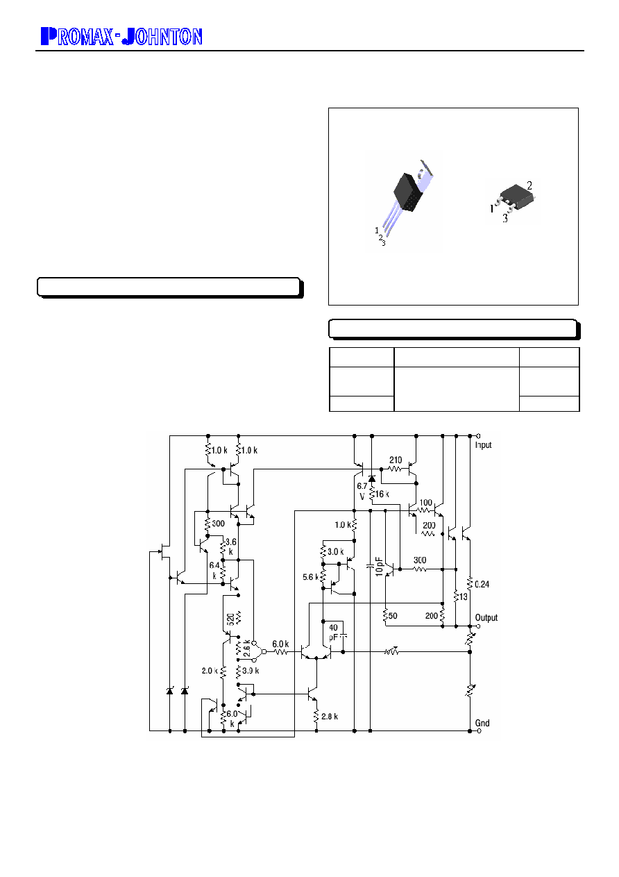
FEATURES
This device contains 28 active transistors
Figure 1.Representative Schematic Diagram
ORDERING INFORMATION
TO-220
TO-252
Pin:1.Input
2.Ground
3.Output

PJ78M00 Series
3-Terminal Medium Current Positive Voltage Regulators
2-10 2001/10.rev.
A
Rating Symbol
Value
Unit
Input Voltage (5.0V-18V)
(20V-24V)
V
I
35
40
Vdc
Power Dissipation (Package Limitation)
Plastic Package, T Suffix
TA=25
Thermal Resistance, Junction-to-Air
Thermal Resistance, Junction-to-Case
Plastic Package, DT Suffix
TA=25
Thermal Resistance, Junction-to-Air
Thermal Resistance,Junction-to-Case
P
D
J
A
J
C
P
D
J
A
J
C
Internally Limited
70
5.0
Internally Limited
92
5.0
/W
/W
/W
/W
Operating Junciton Temperature Range
T
J
+150
Storage Temperatrue Range
Tstg
-65 to +150
1. This device series contains ESD protection and exceeds the following tests:
Human Body Model 2000 V per MIL-STD-883,Method 3015.
Machine Model Method 200V.
Characteristics Symbol
Min
Typ
Max
Unit
Output Voltage (TJ=25)
PJ78M05
Vo 4.9 5.0 5.1 Vdc
Output Voltage Variation
(7.0 Vdc VI20Vdc,5.0mAIo350mA) PJ78M05
Vo
4.8
-
5.2
Vdc
Line Regulation (TJ=25,7.0VdcVI25Vdc,Io=200mA) Regline
- 3.0
50
mV
Load Regulation
(TJ=25,5.0mAIo500mA)
(TJ=25,5.0mAIo200mA)
Regload
-
-
20
10
100
50
mV
Input Bias Current (TJ=25) I
IB
-
3.2
6.0
mA
Quiescent Current Change
(8.0VdcVI25Vdc,Io=200mA)
(5.0mAIo350mA)
I
IB
-
-
-
-
0.8
0.5
mA
Output Noise Voltage (TA=25,10Hzf100kHz)
Vn - 40 - A
Ripple Rejection
(Io=100mA,f=120Hz,9.0VVI19V)
(Io=300mA,f=120Hz,9.0VVI19V,TJ=25)
RR
62
62
-
80
-
-
dB
Dropout Voltage (TJ=25)
VI-Vo - 2.0 - Vdc
Short Circuit Current Limit (TJ=25,VI=35V)
Ios - 50 - mA
Average Temperature Coefficient of Output Voltage
(Io=5.0mA)
Vo/T - ±0.2 -
mV/
Peak Output Current
(TJ=25)
Io - 700 -
mA
2.Tlow=0
for
PJ78Mxx
Thigh=+125 for PJ78Mxx
=-40 for PJ78Mxx
ABSOLUTE MAXIMUM RATINGS
(Ta=25,unless otherwise noted.) (Note 1)
PJ78M05 ELECTRICAL CHARACTERISTICE
(V1=10V,Io=350mA,TJ=Tlow to Thigh,PD5.0W
PJ78M00 Series
3-Terminal Medium Current Positive Voltage Regulators
3-10 2001/10.rev.
A
Characteristics Symbol
Min
Typ
Max
Unit
Output Voltage (TJ=25)
Vo 5.75 6.0 6.25 Vdc
Output Voltage Variation
(8.0 Vdc VI21Vdc,5.0mAIo350mA)
Vo
5.7
-
6.3
Vdc
Line Regulation (TJ=25,8.0VdcVI25Vdc,Io=200mA) Regline - 3.0 50
mV
Load Regulation
(TJ=25,5.0mAIo500mA)
(TJ=25,5.0mAIo200mA)
Regload
-
-
20
10
120
60
mV
Input Bias Current (TJ=25) I
IB
-
3.2
6.0
mA
Quiescent Current Change
(9.0VdcVI25Vdc,Io=200mA)
(5.0mAIo350mA)
I
IB
-
-
-
-
0.8
0.5
mA
Output Noise Voltage (TA=25,10Hzf100kHz)
Vn - 45 - A
Ripple Rejection
(Io=100mA,f=120Hz,9.0VVI19V)
(Io=300mA,f=120Hz,9.0VVI19V,TJ=25)
RR
59
59
-
80
-
-
dB
Dropout Voltage (TJ=25)
VI-Vo - 2.0 - Vdc
Short Circuit Current Limit (TJ=25,VI=35V)
Ios - 50 - mA
Average Temperature Coefficient of Output Voltage (Io=5.0mA)
Vo/T - ±0.2 - mV/
Peak Output Current (TJ=25)
Io - 700 - mA
Characteristics Symbol
Min
Typ
Max
Unit
Output Voltage (TJ=25)
PJ78M08
Vo 7.84 8.0 8.16 Vdc
Output Voltage Variation
(8.0 Vdc VI21Vdc,5.0mAIo350mA)
Vo
7.7
-
8.3
Vdc
Line Regulation (TJ=25,8.0VdcVI25Vdc,Io=200mA) Regline - 60 50
mV
Load Regulation
(TJ=25,5.0mAIo500mA)
(TJ=25,5.0mAIo200mA)
Regload
-
-
25
10
160
80
mV
Input Bias Current (TJ=25) I
IB
-
3.2
6.0
mA
Quiescent Current Change
(10.5VdcVI25Vdc,Io=200mA)
(5.0mAIo350mA)
I
IB
-
-
-
-
0.8
0.5
mA
Output Noise Voltage (TA=25,10Hzf100kHz)
Vn - 52 - V
Ripple Rejection
(Io=100mA,f=120Hz11.5VVI21.5V)
(Io=300mA,f=120Hz,11.5VVI21.5V,TJ=25)
RR
56
56
-
80
-
-
dB
Dropout Voltage (TJ=25)
VI-Vo - 2.0 - Vdc
Short Circuit Current Limit (TJ=25,VI=35V)
Ios - 50 - mA
Average Temperature Coefficient of Output Voltage (Io=5.0mA)
Vo/T - ±0.2 - mV/
Peak Output Current (TJ=25)
Io - 700 - mA
3.Tlow=0
for
PJ78Mxx
Thigh=+125 for PJ78Mxx
=-40 for PJ78Mxx
PJ78M06 ELECTRICAL CHARACTERISTICE
(V1=11V,Io=350mA,0TJ125,PD5.0W,unless otherwise noted
PJ78M08 ELECTRICAL CHARACTERISTICE
(V1=14V,Io=350mA,TJ=Tlow to Thigh,PD5.0W,unless otherwise noted) (Note 3)

PJ78M00 Series
3-Terminal Medium Current Positive Voltage Regulators
4-10 2001/10.rev.
A
Characteristics Symbol
Min
Typ
Max
Unit
Output Voltage (TJ=25)
Vo 8.64 9.0 9.45 Vdc
Output Voltage Variation
(11.5 Vdc VI23Vdc,5.0mAIo350mA)
Vo
8.55
-
9.45
Vdc
Line Regulation (TJ=25,11.5VdcVI25Vdc,Io=200mA) Regline - 60 50 mV
Load Regulation
(TJ=25,5.0mAIo500mA)
(TJ=25,5.0mAIo200mA)
Regload
-
-
25
10
160
90
mV
Input Bias Current (TJ=25) I
IB
-
3.2
6.0
mA
Quiescent Current Change
(11.5VdcVI25Vdc,Io=200mA)
(5.0mAIo350mA)
I
IB
-
-
-
-
0.8
0.5
mA
Output Noise Voltage (TA=25,10Hzf100kHz)
Vn - 52 - V
Ripple Rejection
(Io=100mA,f=120Hz12.5VVI22.5V)
(Io=300mA,f=120Hz,12.5VVI22.5V,TJ=25)
RR
56
56
-
80
-
-
dB
Dropout Voltage (TJ=25)
VI-Vo - 2.0 - Vdc
Short Circuit Current Limit (TJ=25,VI=35V)
Ios - 50 - mA
Average Temperature Coefficient of Output Voltage(Io=5.0mA)
Vo/T - ±0.2 - mV/
Peak Output Current (TJ=25)
Io - 700 - mA
Characteristics Symbol
Min
Typ
Max
Unit
Output Voltage (TJ=25) PJ78M12
Vo
11.76
12
12.24
Vdc
Output Voltage Variation
(14.5 Vdc VI27Vdc,5.0mAIo350mA)
Vo
11.5
-
12.5
Vdc
Line Regulation (TJ=25,11.5VdcVI25Vdc,Io=200mA) Regline - 80 50 mV
Load Regulation
(TJ=25,5.0mAIo500mA)
(TJ=25,5.0mAIo200mA)
Regload
-
-
25
10
240
120
mV
Input Bias Current (TJ=25) I
IB
-
3.2
6.0
mA
Quiescent Current Change
(14.5VdcVI30Vdc,Io=200mA)
(5.0mAIo350mA)
I
IB
-
-
-
-
0.8
0.5
mA
Output Noise Voltage (TA=25,10Hzf100kHz)
Vn - 75 - V
Ripple Rejection
(Io=100mA,f=120Hz15VVI25V)
(Io=300mA,f=120Hz,15VVI25V,TJ=25)
RR
55
55
-
80
-
-
dB
Dropout Voltage (TJ=25)
VI-Vo - 2.0 - Vdc
Short Circuit Current Limit (TJ=25,VI=35V)
Ios - 50 - mA
Average Temperature Coefficient of Output Voltage(Io=5.0mA)
Vo/T - ±0.3 - mV/
Peak Output Current (TJ=25)
Io - 700 - mA
4. Tlow=0
for
PJ78Mxx
Thigh=+125 for PJ78Mxx
=-40 for PJ78Mxx
PJ78M09 ELECTRICAL CHARACTERISTICE
(V1=15V,Io=350mA,TJ=Tlow to Thigh,PD5.0W,unless otherwise noted) (Note 4)
PJ78M12 ELECTRICAL CHARACTERISTICE
(V1=19V,Io=350mA,TJ=Tlow to Thigh,PD5.0W,unless otherwise noted) (Note 4)
PJ78M00 Series
3-Terminal Medium Current Positive Voltage Regulators
5-10 2001/10.rev.
A
Characteristics Symbol
Min
Typ
Max
Unit
Output Voltage (TJ=25) PJ78M15
Vo
14.7
15
15.3
Vdc
Output Voltage Variation
(17.5 Vdc VI30Vdc,5.0mAIo350mA)
Vo
14.4
-
15.6
Vdc
Line Regulation (TJ=25,17.5VdcVI30Vdc,Io=200mA) Regline - 10 50 mV
Load Regulation
(TJ=25,5.0mAIo500mA)
(TJ=25,5.0mAIo200mA)
Regload
-
-
25
10
300
150
mV
Input Bias Current (TJ=25) I
IB
-
3.2
6.0
mA
Quiescent Current Change
(17.8VdcVI30Vdc,Io=200mA)
(5.0mAIo350mA)
I
IB
-
-
-
-
0.8
0.5
mA
Output Noise Voltage (TA=25,10Hzf100kHz)
Vn - 90 - V
Ripple Rejection
(Io=100mA,f=120Hz,18.5VVI28.5V)
(Io=300mA,f=120Hz,18.5VVI28.5V,TJ=25)
RR
54
54
-
70
-
-
dB
Dropout Voltage (TJ=25)
VI-Vo - 2.0 - Vdc
Short Circuit Current Limit (TJ=25,VI=35V)
Ios - 50 - mA
Average Temperature Coefficient of Output Voltage(Io=5.0mA)
Vo/T - ±0.3 - mV/
Peak Output Current (TJ=25)
Io - 700 - mA
Characteristics Symbol
Min
Typ
Max
Unit
Output Voltage (TJ=25)
Vo
17.3
18
18.7
Vdc
Output Voltage Variation
(21 Vdc VI33Vdc,5.0mAIo350mA)
Vo
17.1
-
18.9
Vdc
Line Regulation (TJ=25,17.5VdcVI30Vdc,Io=200mA) Regline - 10 50 mV
Load Regulation
(TJ=25,5.0mAIo500mA)
(TJ=25,5.0mAIo200mA)
Regload
-
-
30
10
360
180
mV
Input Bias Current (TJ=25) I
IB
-
3.2
6.5
mA
Quiescent Current Change
(21VdcVI33Vdc,Io=200mA)
(5.0mAIo350mA)
I
IB
-
-
-
-
0.8
0.5
mA
Output Noise Voltage (TA=25,10Hzf100kHz)
Vn - 100 - V
Ripple Rejection
(Io=100mA,f=120Hz,22VVI32V)
(Io=300mA,f=120Hz,22VVI32V,TJ=25)
RR
53
53
-
70
-
-
dB
Dropout Voltage (TJ=25)
VI-Vo - 2.0 - Vdc
Short Circuit Current Limit (TJ=25,VI=35V)
Ios - 50 - mA
Average Temperature Coefficient of Output Voltage (Io=5.0mA)
Vo/T - ±0.3 - mV/
Peak Output Current (TJ=25)
Io - 700 - mA
5. Tlow=0
for
PJ78Mxx
Thigh=+125 for PJ78Mxx
=-40 for PJ78Mxx
PJ78M15 ELECTRICAL CHARACTERISTICE
(V1=23V,Io=350mA,TJ=Tlow to Thigh,PD5.0W,unless otherwise noted) (Note 5)
PJ78M18 ELECTRICAL CHARACTERISTICE
(V1=27V,Io=350mA,TJ=Tlow to Thigh,PD5.0W,unless otherwise noted)