PLL500-27B/-37B/-47B
Low Power CMOS Output VCXO Family (27MHz to 200MHz)
47745 Fremont Blvd., Fremont, California 94538 TEL (510) 492-0990 FAX (510) 492-0991
Rev 09/13/04 Page 1
FEATURES
∑ VCXO output for the 27MHz to 200MHz range
- PLL500-27: 27MHz to 65MHz
- PLL500-37: 65MHz to 130MHz
- PLL500-47: 100MHz to 200MHz
∑ Low phase noise (-130 dBc @ 10kHz offset).
∑ CMOS output with OE tri-state control.
∑ Selectable output drive (Standard or High drive).
- Standard: 12mA drive capability at TTL level.
- High: 36mA drive capability at TTL level.
∑ Fundamental crystal input.
∑ Integrated high linearity variable capacitors.
∑ +/- 150 ppm pull range, max 5% linearity.
∑ Low jitter (RMS): 2.5ps period jitter.
∑ 2.5-3.3V operation.
∑ Available in 8-Pin SOIC or DIE.
DESCRIPTION
The PLL500-27/-37/-47 are a low cost, high perform-
ance, low phase noise, and high linearity VCXO fam-
ily for the 27 to 200MHz range, providing less than -
130dBc at 10kHz offset. The very low jitter (2.5 ps
RMS period jitter) makes these chips ideal for appli-
cations requiring voltage controlled frequency
sources. The IC's are designed to accept fundamen-
tal resonant mode crystals.
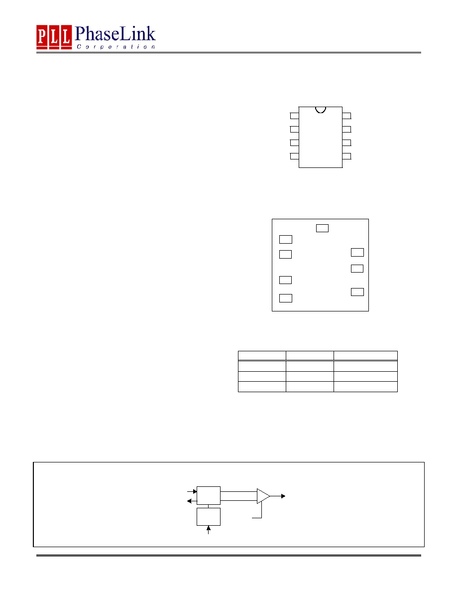
PIN CONFIGURATION
DIE PAD LAYOUT
FREQUENCY RANGE
PART #
MULTIPLIER
FREQUENCY
PLL500-27B
No PLL
27 ≠ 65 MHz
PLL500-37B
No PLL
65 ≠ 130 MHz
PLL500-47B
No PLL
100 ≠ 200 MHz
BLOCK DIAGRAM
P500-x7B
1
2
3
4
5
6
7
8
XIN
OE^
VIN
GND
XOUT
VDD*
CLK
DS^
^: Denotes internal Pull-up
1
2
3
4
7
6
5
8
Die ID:
PLL500-27B:
C500A0505-05P
PLL500-37BDC:
C500A0505-05Q
PLL500-47BDC:
C500A0505-05R
PLL500-27B/-37B/-47B
Low Power CMOS Output VCXO Family (27MHz to 200MHz)
47745 Fremont Blvd., Fremont, California 94538 TEL (510) 492-0990 FAX (510) 492-0991
Rev 09/13/04 Page 2
PIN AND PAD DESCRIPTION
Die Pad Position
Name Pin#
X (
µm) Y
(
µm)
Type Description
XIN
1
94.183
768.599
I
Crystal input pin.
OE 2
94.157 605.029 I
Output Enable input pin. Disables the output when low. Internal
pull-up enables output by default if pin is not connected low.
VCON
3
94.183
331.756
I
Frequency control voltage input pin.
GND 4
94.193
140.379
P
Ground
pin.
CLK
5
715.472
203.866
O
Output clock pin.
VDD
6
715.307
455.726
P
VDD power supply pin.
DRIVSEL 7 715.472 626.716 I
Output drive select pin. High drive if set to `0'. Low drive if set
to `1'. Internal pull-up.
XOUT 8
476.906
888.881 I
Crystal
output pin. Ref clock input.
ELECTRICAL SPECIFICATIONS
1. Absolute Maximum Ratings
PARAMETERS SYMBOL
MIN.
MAX.
UNITS
Supply Voltage Range
V
CC
-
0.5
4.6 V
Input Voltage Range
V
I
-
0.5 V
CC
+
0.5
V
Output Voltage Range
V
O
-
0.5 V
CC
+
0.5
V
Soldering Temperature
240
∞C
Storage Temperature
T
S
-65 150
∞C
Ambient Operating Temperature
-40
+85
∞C
Exposure of the device under conditions beyond the limits specified by Maximum Ratings for extended periods may cause permanent damage to the
device and affect product reliability. These conditions represent a stress rating only, and functional operations of the device at these or any other
conditions above the operational limits noted in this specification is not implied.
PLL500-27B/-37B/-47B
Low Power CMOS Output VCXO Family (27MHz to 200MHz)
47745 Fremont Blvd., Fremont, California 94538 TEL (510) 492-0990 FAX (510) 492-0991
Rev 09/13/04 Page 3
2. AC Electrical Specifications
PARAMETERS SYMBOL CONDITIONS MIN.
TYP.
MAX.
UNITS
PLL500-27
27 65
PLL500-37 65
130
Input Crystal Frequency
PLL500-47
100 200
MHz
0.8V ~ 2.0V with 10 pF load
1.15
Output Clock Rise/Fall Time
0.3V ~ 3.0V with 15 pF load
3.7
ns
Output Clock Duty Cycle
Measured @ 1.4V
45
50
55
%
Short Circuit Current
±50
mA
3. Voltage Control Crystal Oscillator
PARAMETERS SYMBOL CONDITIONS MIN.
TYP.
MAX.
UNITS
VCXO Stabilization Time *
T
VCXOSTB
From power valid
10 ms
VCXO Tuning Range
XTAL C
0
/C
1
< 250
300
ppm
CLK output pullability
0V
VCON 3.3V
±150
ppm
VCXO Tuning Characteristic
100 ppm/V
Pull range linearity
5
%
Power Supply Rejection
PWSRR
Frequency change with
VDD varied +/- 10%
-1 +1
ppm
VCON pin input impedance
2000
k
VCON modulation BW
0V
VCON 3.3V, -3dB
45
kHz
Note: Preliminary Specifications still to be characterized. Parameters denoted with an asterisk (*) represent nominal characterization data and are not
production tested to any specific limits.
4. Jitter and Phase Noise specification
PARAMETERS CONDITIONS
MIN.
TYP.
MAX.
UNITS
RMS Period Jitter
(1 sigma ≠ 1000 samples)
With capacitive decoupling
between VDD and GND.
2.5 ps
Phase Noise relative to carrier
@100Hz
offset
-80 dBc/Hz
Phase Noise relative to carrier
@1kHz
offset
-110 dBc/Hz
Phase Noise relative to carrier
@10kHz
offset
-130 dBc/Hz
Phase Noise relative to carrier
@100kHz
offset
-138 dBc/Hz
Phase Noise relative to carrier
@1MHz
offset
-145 dBc/Hz
PLL500-27B/-37B/-47B
Low Power CMOS Output VCXO Family (27MHz to 200MHz)
47745 Fremont Blvd., Fremont, California 94538 TEL (510) 492-0990 FAX (510) 492-0991
Rev 09/13/04 Page 4
5. DC Specification
PARAMETERS SYMBOL
CONDITIONS
MIN. TYP. MAX.
UNITS
F
XIN
= 36MHz, 15pF output load
5
6
F
XIN
= 77MHz, 15pF output load
10
12
Supply Current, Dynamic,
with Loaded Outputs
I
DD
F
XIN
= 155MHz, 15pF output load
15
18
mA
PLL500-27
N/A
pF
PLL500-37 and-47: Std drive
15
pF
Allowable output load
capacitance
C
L
(Output)
PLL500-37 and-47: High drive
10
pF
Operating Voltage
V
DD
2.25 3.63
V
Output High Voltage
V
OH
I
OH
= -12mA
2.4
V
Output Low Voltage
V
OL
I
OL
= 12mA
0.4
V
Output High Voltage at
CMOS level
I
OH
= -4mA
V
DD
≠ 0.4
V
Standard drive at TTL level
12
17
Output drive current
High drive at TTL level
36
51
mA
Short Circuit Current
±50
mA
VCXO Control Voltage
VCON
0
3.3
V
ESD Protection
Human Body Model
2000
V
6. Crystal Specifications
PARAMETERS SYMBOL
MIN.
TYP.
MAX.
UNITS
Crystal Loading Rating (VCON = 1.65V)
C
L
(xtal)
8.5 pF
Maximum Sustainable Drive Level
200
µW
Operating Drive Level
50
µW
Max C0 for PLL500-27
3.5
Max C0 for PLL500-37
2.5
Max C0 for PLL500-47
2
pF
C0/C1
250
-
ESR R
S
30
Note: The crystal must be such that it oscillates (parallel resonant) at nominal frequency when presented a C Load as specified above.
If the crystal requires more load to be at nominal frequency, the additional load must be added externally.
This however may reduce the pull range.
PLL500-27B/-37B/-47B
Low Power CMOS Output VCXO Family (27MHz to 200MHz)
47745 Fremont Blvd., Fremont, California 94538 TEL (510) 492-0990 FAX (510) 492-0991
Rev 09/13/04 Page 5
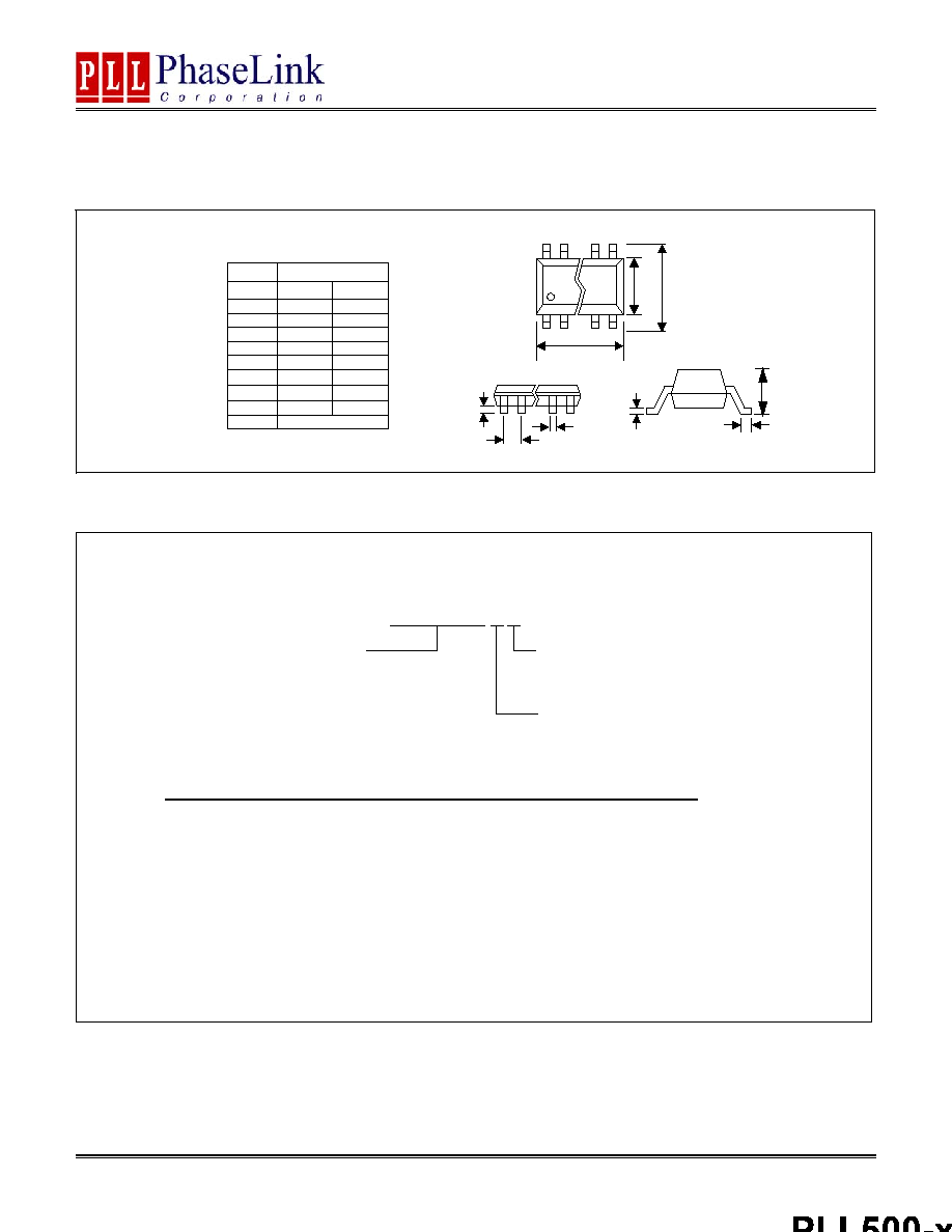
PACKAGE INFORMATION
ORDERING INFORMATION
PhaseLink Corporation, reserves the right to make changes in its products or specifications, or both at any time without notice. The information fur-
nished by Phaselink is believed to be accurate and reliable. However, PhaseLink makes no guarantee or warranty concerning the accuracy of said
information and shall not be responsible for any loss or damage of whatever nature resulting from the use of, or reliance upon this product.
LIFE SUPPORT POLICY: PhaseLink's products are not authorized for use as critical components in life support devices or systems without the ex-
press written approval of the President of PhaseLink Corporation.
C
L
A
8 PIN ( dimensions in mm )
Narrow SOIC
Symbol
Min.
Max.
A
1.47
1.73
A1
0.10
0.25
B
0.33
0.51
C
0.19
0.25
D
4.80
4.95
E
3.80
4.00
H
5.80
6.20
L
0.38
1.27
e
1.27 BSC
E
H
D
A
1
e
B
PART NUMBER
The order number for this device is a combination of the following:
Device number, Package type and Operating temperature range
Order Number
Marking
Package Option
PLL500-27BSC P500-27B
SC
8-Pin SOIC (Tube)
PLL500-27BSC-R P500-27B SC
8-Pin SOIC (Tape and Reel)
PLL500-27BDC P500-27B
DC Die
(Waffle
Pack)
PLL500-37BSC P500-37B
SC
8-Pin SOIC (Tube)
PLL500-37BSC-R P500-37B SC
8-Pin SOIC (Tape and Reel)
PLL500-37BDC P500-37B
DC Die
(Waffle
Pack)
PLL500-47BSC P500-47B
SC
8-Pin SOIC (Tube)
PLL500-47BSC-R P500-47B SC
8-Pin SOIC (Tape and Reel)
PLL500-47BDC P500-47B
DC Die
(Waffle
Pack)