 | –≠–ª–µ–∫—Ç—Ä–æ–Ω–Ω—ã–π –∫–æ–º–ø–æ–Ω–µ–Ω—Ç: P502-26SC | –°–∫–∞—á–∞—Ç—å:  PDF PDF  ZIP ZIP |

PLL502-26
High Pull-Range VCXO (27MHz) with integrated Audio PLL
47745 Fremont Blvd., Fremont, California 94538 Tel (510) 492-0990 Fax (510) 492-0991 www.phaselink.com Rev 09/17/04 Page 1
XTAL
OSC
XIN
XOUT
OUT_27MHz
VCON
VARICAP
10X
PLL
REF_Audio
OUT_Audio
FEATURES
∑ Low phase noise 27MHz VCXO (-135 dBc at
10kHz offset).
∑ Integrated variable capacitors.
∑ Wide pull range (+/- 250 ppm).
∑ Low jitter (RMS): 10ps period.
∑ Integrated audio Phase Locked Loop.
∑ Audio clock output (ideal for 8.192MHz,
11.2896MHz, 12.288MHz).
∑ 27MHz crystal input.
∑ Audio Reference clock input.
∑ 3.3V operation.
∑ Available in 16-Pin SOIC.
DESCRIPTION
The PLL502-26 is a low cost, high pull-range and
low phase noise VCXO, providing less than -135dBc
at 10kHz offset at 27MHz. It also integrates an Audio
clock phase locked loop ideal for the 8.192MHz,
11.2896MHz and 12.288MHz audio outputs, starting
from an audio reference clock. Its very high pull
range makes it ideal for Digital Video applications,
allowing users to save board space and cost.
PIN CONFIGURATION
PLL502-26
1
2
3
4
5
6
7
8
N/C*
9
1
0
1
1
1
2
1
3
1
4
1
5
1
6
VDD_PLL
VDD_VCXO
XIN
XOUT
VCON
GND_PLL
N/C*
GND_27MHz
OUT_27MHz
VDD_27MHz
VDD_Audio
OUT_Audio
GND_Audio
REF_Audio
GND_VCXO
Note: * Pins reserved for future DAC integration
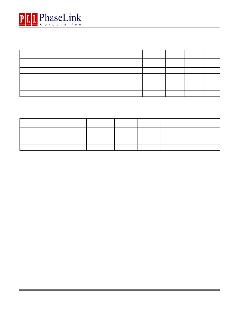
OUTPUT RANGE
OUTPUT FREQUENCY
RANGE OUTPUT
TYPE
VCXO 27MHz CMOS
Audio
8.192MHz ≠ 12.288MHz
CMOS
BLOCK DIAGRAM

PLL502-26
High Pull-Range VCXO (27MHz) with integrated Audio PLL
47745 Fremont Blvd., Fremont, California 94538 Tel (510) 492-0990 Fax (510) 492-0991 www.phaselink.com Rev 09/17/04 Page 2
PIN DESCRIPTIONS
Name Number
Type
Description
N/C 1,16
No
connection.
VDD_PLL 2 P
VDD power supply pin for PLL circuitry. This pin should be decoupled sepa-
rately from other VDD.
VDD_VCXO 3 P
VDD power supply pin for VCXO circuitry. This pin should be decoupled
separately from other VDD.
XIN
4
I
Crystal input. See Crystal Specifications on page 4.
XOUT
5
O
Crystal output. See Crystal Specifications on page 4.
VCON 6
I
Voltage
Control
input.
GND_VCXO
7
P
GND connection for VCXO circuitry.
GND_PLL
8
P
GND connection for VCXO circuitry.
REF_Audio
9
I
Audio Reference Clock input.
GND_Audio
10
P
GND connection for Audio clock output buffer circuitry.
OUT_Audio
11
O
Audio clock output.
VDD_Audio 12 P
VDD power supply pin for Audio clock output buffer. This pin should be
decoupled separately from other VDD.
VDD_27MHz 13 P
VDD power supply pin for 27MHz output clock. This pin should be decoup-
led separately from other VDD.
OUT_27MHz
14
O
27MHz VCXO output clock.
GND_27MHz
15
P
GND connection for 27MHz output buffer circuitry.
ELECTRICAL SPECIFICATIONS
1. Absolute Maximum Ratings
PARAMETERS SYMBOL
MIN.
MAX.
UNITS
Supply Voltage
V
DD
4.6 V
Input Voltage, dc
V
I
-0.5
V
DD
+0.5 V
Output Voltage, dc
V
O
-0.5
V
DD
+0.5 V
Storage Temperature
T
S
-65 150
∞C
Ambient Operating Temperature*
T
A
-40 85
∞C
Junction Temperature
T
J
125
∞C
Lead Temperature (soldering, 10s)
260
∞C
ESD Protection, Human Body Model
2
kV
Exposure of the device under conditions beyond the limits specified by Maximum Ratings for extended periods may cause permanent damage to the
device and affect product reliability. These conditions represent a stress rating only, and functional operations of the device at these or any other
conditions above the operational limits noted in this specification is not implied.
* Note: Operating Temperature is guaranteed by design for all parts (COMMERCIAL and INDUSTRIAL), but tested for COMMERCIAL grade only.

PLL502-26
High Pull-Range VCXO (27MHz) with integrated Audio PLL
47745 Fremont Blvd., Fremont, California 94538 Tel (510) 492-0990 Fax (510) 492-0991 www.phaselink.com Rev 09/17/04 Page 3
2. AC Electrical Specifications
PARAMETERS SYMBOL CONDITIONS MIN.
TYP.
MAX.
UNITS
Input Crystal Frequency
27
MHz
Audio Reference Clock
REF_Audio
0.65
-
1.5
MHz
Output Clock Rise/Fall Time
0.3V ~ 3.0V with 15 pF load
2
ns
Output Clock Duty Cycle
Measured @ 50% V
DD
45
50
55
%
3. Voltage Control Crystal Oscillator
PARAMETERS SYMBOL CONDITIONS MIN.
TYP.
MAX.
UNITS
VCXO Stabilization Time *
T
VCXOSTB
From power valid
10
ms
VCXO Tuning Range
F
XIN
= 12 ≠ 27MHz;
XTAL C
0
/C
1
< 250
0V
VIN 3.3V
500 ppm
CLK output pullability
VCON=1.65V
±1.65V
±250
ppm
VCXO Tuning Characteristic
150
ppm/V
Pull range linearity
10
%
VCON pin input impedance
2000
k
VCON modulation BW
0V
VIN 3.3V, -3dB
25
kHz
Note: Parameters denoted with an asterisk (*) represent nominal characterization data and are not production tested to any specific limits.
4. Jitter and Phase Noise Specification
PARAMETERS CONDITIONS
MIN.
TYP.
MAX.
UNITS
RMS Period Jitter
(1 sigma ≠ 10,000 samples)
with capacitive decoupling
between VDD and GND.
3
ps
Phase Noise relative to carrier
27MHz @100Hz offset
-85
dBc/Hz
Phase Noise relative to carrier
27MHz @1kHz offset
-115
dBc/Hz
Phase Noise relative to carrier
27MHz @10kHz offset
-135
dBc/Hz
Phase Noise relative to carrier
27MHz @100kHz offset
-140
dBc/Hz
Phase Noise relative to carrier
27MHz @1MHz offset
-150
dBc/Hz
PLL502-26
High Pull-Range VCXO (27MHz) with integrated Audio PLL
47745 Fremont Blvd., Fremont, California 94538 Tel (510) 492-0990 Fax (510) 492-0991 www.phaselink.com Rev 09/17/04 Page 4
5. DC Specification
PARAMETERS SYMBOL
CONDITIONS
MIN. TYP. MAX.
UNITS
Supply Current, Dynamic,
with Loaded Outputs
I
DD
F
XIN
= 12 - 27MHz
Ouput load of 10pF
30
35
mA
Operating Voltage
V
DD
2.97
3.63
V
I
OH
V
OH
= V
DD
-0.4V, V
DD
=3.3V 10
mA
Output drive current
I
OL
V
OL
= 0.4V, V
DD
= 3.3V
10
mA
Short Circuit Current
±50
mA
VCXO Control Voltage
VCON
0
3.3
V
6. Crystal Specifications
PARAMETERS SYMBOL
MIN.
TYP.
MAX.
UNITS
Crystal Resonator Frequency
F
XIN
27
MHz
Crystal Loading Capacitance Rating
C
L
(xtal)
9.5
pF
C0/C1
250
-
ESR R
S
30
Note: Crystal Loading rating: 9.5pF is the loading the crystal sees from the VCXO chip at VCON = 1.65V. It is assumed that the crystal will be at
nominal frequency at this load. If the crystal requires more load to be at nominal frequency, the additional load must be added externally.
This however may reduce the pull range.

PLL502-26
High Pull-Range VCXO (27MHz) with integrated Audio PLL
47745 Fremont Blvd., Fremont, California 94538 Tel (510) 492-0990 Fax (510) 492-0991 www.phaselink.com Rev 09/17/04 Page 5
PACKAGE INFORMATION
ORDERING INFORMATION
PhaseLink Corporation, reserves the right to make changes in its products or specifications, or both at any time without notice. The information fur-
nished by Phaselink is believed to be accurate and reliable. However, PhaseLink makes no guarantee or warranty concerning the accuracy of said
information and shall not be responsible for any loss or damage of whatever nature resulting from the use of, or reliance upon this product.
LIFE SUPPORT POLICY: PhaseLink's products are not authorized for use as critical components in life support devices or systems without the ex-
press written approval of the President of PhaseLink Corporation.
PART NUMBER
The order number for this device is a combination of the following:
Device number, Package type and Operating temperature range
PLL502-26
S
C
Order Number
Marking
Package
t
PLL502-26SC P502-26SC
SOIC - Tube
PLL502-26SC-R P502-26SC
SOIC (Tape & Reel)
PART NUMBER
TEMPERATURE
C=COMMERCIAL
PACKAGE TYPE
S=SOIC
C
L
A
E
H
D
A1
e
B
16 PIN Narrow SOIC ( mm )
SOIC
Symbol
Min.
Max.
A
1.35
1.75
A1
0.10
0.25
B
0.33
0.51
C
0.19
0.25
D
9.80
10.00
E
3.80
4.00
H
5.80
6.20
L
0.40
1.27
e
1.27 BSC