PLL502-35/-37/-38/-39
750kHz ≠ 800MHz Low Phase Noise Multiplier VCXO
Universal Low Phase Noise IC's
47745 Fremont Blvd., Fremont, California 94538 Tel (510) 492-0990 Fax (510) 492-0991 www.phaselink.com Rev 01/19/06 Page 1
FEATURES
∑ Selectable 750kHz to 800MHz range.
∑ Low phase noise output (@ 10kHz frequency
offset, -142dBc/Hz for 19.44MHz, -125dBc/Hz for
155.52MHz, -115dBc/Hz for 622.08MHz).
∑ CMOS (PLL502-37), PECL (PLL502-35 and
PLL502-38) or LVDS (PLL502-39) output.
∑ 12 to 25MHz crystal input.
∑ No external load capacitor or varicap required.
∑ Output Enable selector.
∑ Wide pull range (+/-200 ppm)
∑ Selectable 1/16 to 32x frequency multiplier.
∑ 3.3V operation.
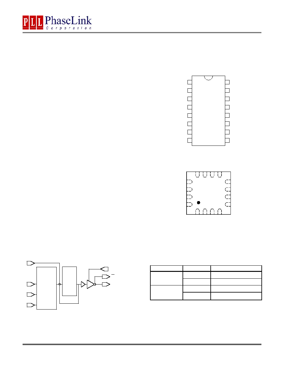
∑ Available in 16-Pin (TSSOP or 3x3mm QFN).
DESCRIPTION
The PLL502-35 (PECL with inverted OE), PLL502-37
(CMOS), PLL502-38 (PECL), and PLL502-39 (LVDS)
are high performance and low phase noise VCXO IC
chips. They provide phase noise performance as low
as ≠125dBc at 10kHz offset (at 155MHz), by multi-
plying the input crystal frequency up to 32x. The
wide pull range (+/- 200 ppm) and very low jitter
make them ideal for a wide range of applications,
including SONET/SDH and FEC. They accept fun-
damental parallel resonant mode crystals from 12 to
25MHz.
BLOCK DIAGRAM
PIN CONFIGURATION
(Top View)
^: Internal
pull-up
*: On 3x3 package, PLL502-35/-38 do not have SEL0 available: Pin
10 is VDD, pin 11 is GND. However, PLL502-37/-39 have SEL0
(pin 10), and pin11 is VDD. See pin assignment table for details.
OUTPUT ENABLE LOGICAL LEVELS
Part #
OE
State
0 (Default)
Output enabled
PLL502-38
1 Tri-state
0 Tri-state
PLL502-35
PLL502-37
PLL502-39
1 (Default)
Output enabled
OE input: Logical states defined by PECL levels for PLL502-38
Logical states defined by CMOS levels for PLL502-37/-39
PLL 502-3x
1
2
3
4
5
6
7
8
VDD
9
10
11
12
13
14
15
16
XIN
XOUT
SEL3^
SEL2^
OE
VCON
GND
SEL0^
SEL1^
GND
CLKC
VDD
CLKT
GND
GND
P502-3x
GND
VDD
CLKT
CLKC
1
2
3
4
12
11
10
9
13
14
15
16
8
7
6
5
XI
N
SEL
0^
/ VDD*
SE
L
1
^
VD
D /
GND
*
SEL3^
XOUT
SEL2^
OE
GND
VC
O
N
GND
GND
X+
X-
OE
Q
PLL502-3x
Vin
Q
PLL by-pass
SEL
PLL
(Phase
Locked
Loop)
Oscillator
Amplifier
w/
integrated
varicaps
PLL502-35/-37/-38/-39
750kHz ≠ 800MHz Low Phase Noise Multiplier VCXO
Universal Low Phase Noise IC's
47745 Fremont Blvd., Fremont, California 94538 Tel (510) 492-0990 Fax (510) 492-0991 www.phaselink.com Rev 01/19/06 Page 2
FREQUENCY SELECTION TABLE
SEL3
SEL2 SEL1 SEL0
Selected
Multiplier
0
0
1
1
Fin x 32
0 1 1 0
Fin
/
8
0
1
1
1
Fin x 2
1 0 0 1
Fin
/
2
1 0 1 0
Fin
/
16
1
0
1
1
Fin x 4
1 1 0 0
Fin
/
4
1
1
0
1
Fin x 8
1
1
1
0
Fin x 16
1 1 1 1
No
multiplication
Note: SEL0 is not available (always "1") for PLL502-35 and PLL502-38 in 3x3mm package
PIN DESCRIPTIONS PLL502-35 and PLL502-38 (see next page of PLL502-37/-39)
Name
TSSOP
Pin number
3x3mm QFN
Pin number
Type Description
XIN
2
12
I
Crystal input. See Crystal Specification on page 4.
XOUT
3
13
I
Crystal output. See Crystal Specification on page 4.
OE
6
16
I
Output enable pin (see OE logic state table on page 1).
VCON 7
1
I
Voltage
Control
input.
GND 8,9,10,14
2,3,4,8,11
P
Ground.
CLKT 11
5
O
True
output
PECL
CLKC 13
7
O
Complementary
output
PECL.
SEL0 16
Not
available
I
SEL1 15
9
I
SEL2 5
15
I
SEL3 4
14
I
Multiplier selector pins. These pins have an internal pull-up
that will default SEL to `1' when not connected to GND.
VDD
1, 12
6,10
P
+3.3V power supply.
PLL502-35/-37/-38/-39
750kHz ≠ 800MHz Low Phase Noise Multiplier VCXO
Universal Low Phase Noise IC's
47745 Fremont Blvd., Fremont, California 94538 Tel (510) 492-0990 Fax (510) 492-0991 www.phaselink.com Rev 01/19/06 Page 3
PIN DESCRIPTIONS PLL502-37/-39 (see previous page of PLL502-35/-38)
Name
TSSOP
Pin number
3x3mm QFN
Pin number
Type Description
XIN
2
12
I
Crystal input. See Crystal Specification on page 4.
XOUT
3
13
I
Crystal output. See Crystal Specification on page 4.
OE
6
16
I
Output enable pin (see OE logic state table on page 1).
VCON 7 1 I
Voltage
Control
input.
GND 8,9,10,14 2,3,4,8 P
Ground.
CLKT 11 5
O
True output LVDS (PLL502-39)
(N/C for PLL502-37)
CLKC 13 7 O
Complementary output LVDS (PLL502-39)
(CMOS out for PLL502-37).
SEL0 16 10
I
SEL1 15 9 I
SEL2 5 15
I
SEL3 4 14
I
Multiplier selector pins. These pins have an internal pull-up
that will default SEL to `1' when not connected to GND.
VDD
1, 12
6,11
P
+3.3V power supply.
ELECTRICAL SPECIFICATIONS
1. Absolute Maximum Ratings
PARAMETERS SYMBOL
MIN.
MAX.
UNITS
Supply Voltage
V
DD
4.6 V
Input Voltage, dc
V
I
-0.5
V
DD
+0.5 V
Output Voltage, dc
V
O
-0.5
V
DD
+0.5 V
Storage Temperature
T
S
-65 150
∞C
Ambient Operating Temperature*
T
A
-40 85
∞C
Junction Temperature
T
J
125
∞C
Lead Temperature (soldering, 10s)
260
∞C
ESD Protection, Human Body Model
2
kV
Exposure of the device under conditions beyond the limits specified by Maximum Ratings for extended periods may cause permanent damage to the
device and affect product reliability. These conditions represent a stress rating only, and functional operations of the device at these or any other con-
ditions above the operational limits noted in this specification is not implied.
* Note: Operating Temperature is guaranteed by design for all parts (COMMERCIAL and INDUSTRIAL), but tested for COMMERCIAL grade only.
PLL502-35/-37/-38/-39
750kHz ≠ 800MHz Low Phase Noise Multiplier VCXO
Universal Low Phase Noise IC's
47745 Fremont Blvd., Fremont, California 94538 Tel (510) 492-0990 Fax (510) 492-0991 www.phaselink.com Rev 01/19/06 Page 4
2. Crystal Specifications
PARAMETERS SYMBOL CONDITIONS MIN.
TYP.
MAX.
UNITS
Crystal Resonator Frequency
F
XIN
Parallel Fundamental Mode
12
25
MHz
Crystal Loading Rating
C
L (xtal)
At VCON = 1.65V
9.5
pF
Crystal Pullability
C
0
/C
1 (xtal)
AT
cut
250
-
Recommended ESR
R
E
AT cut
30
Note: Crystal Loading rating: 9.5pF is the loading the crystal sees from the VCXO chip at VCON = 1.65V. It is assumed that the crystal will be at nomi-
nal frequency at this load. If the crystal requires more load to be at nominal frequency, the additional load must be added externally. This however may
reduce the pull range.
3. Voltage Control Crystal Oscillator
PARAMETERS SYMBOL CONDITIONS MIN.
TYP.
MAX.
UNITS
VCXO Stabilization Time *
T
VCXOSTB
From power valid
10 ms
VCXO Tuning Range
F
XIN
= 12 ≠ 25MHz;
XTAL C
0
/C
1
< 250
0V
VCON 3.3V
500 ppm
CLK output pullability
VCON=1.65V,
±1.65V
±200
ppm
VCXO Tuning Characteristic
150
ppm/V
Pull range linearity
10
%
VCON pin input impedance
2000
k
VCON modulation BW
0V
VCON 3.3V, -3dB
25
kHz
Note: Parameters denoted with an asterisk (*) represent nominal characterization data and are not production tested to any specific limits.
4. General Electrical Specifications
PARAMETERS SYMBOL
CONDITIONS
MIN. TYP. MAX. UNITS
Fout<24MHz
60/28/15
24MHz<Fout<96MHz
65/45/30
Supply Current,
Dynamic (with
Loaded Outputs)
I
DD
PECL/LVDS/CMOS
96MHz<Fout<800MHz
100/80/40
mA
Operating Voltage
V
DD
2.97
3.63 V
Output Clock
Duty Cycle
@ 50% V
DD
(CMOS)
@ 1.25V (LVDS)
@
V
DD
≠ 1.3V (PECL)
45
45
45
50
50
50
55
55
55
%
Short Circuit
Current
±50
mA
PLL502-35/-37/-38/-39
750kHz ≠ 800MHz Low Phase Noise Multiplier VCXO
Universal Low Phase Noise IC's
47745 Fremont Blvd., Fremont, California 94538 Tel (510) 492-0990 Fax (510) 492-0991 www.phaselink.com Rev 01/19/06 Page 5
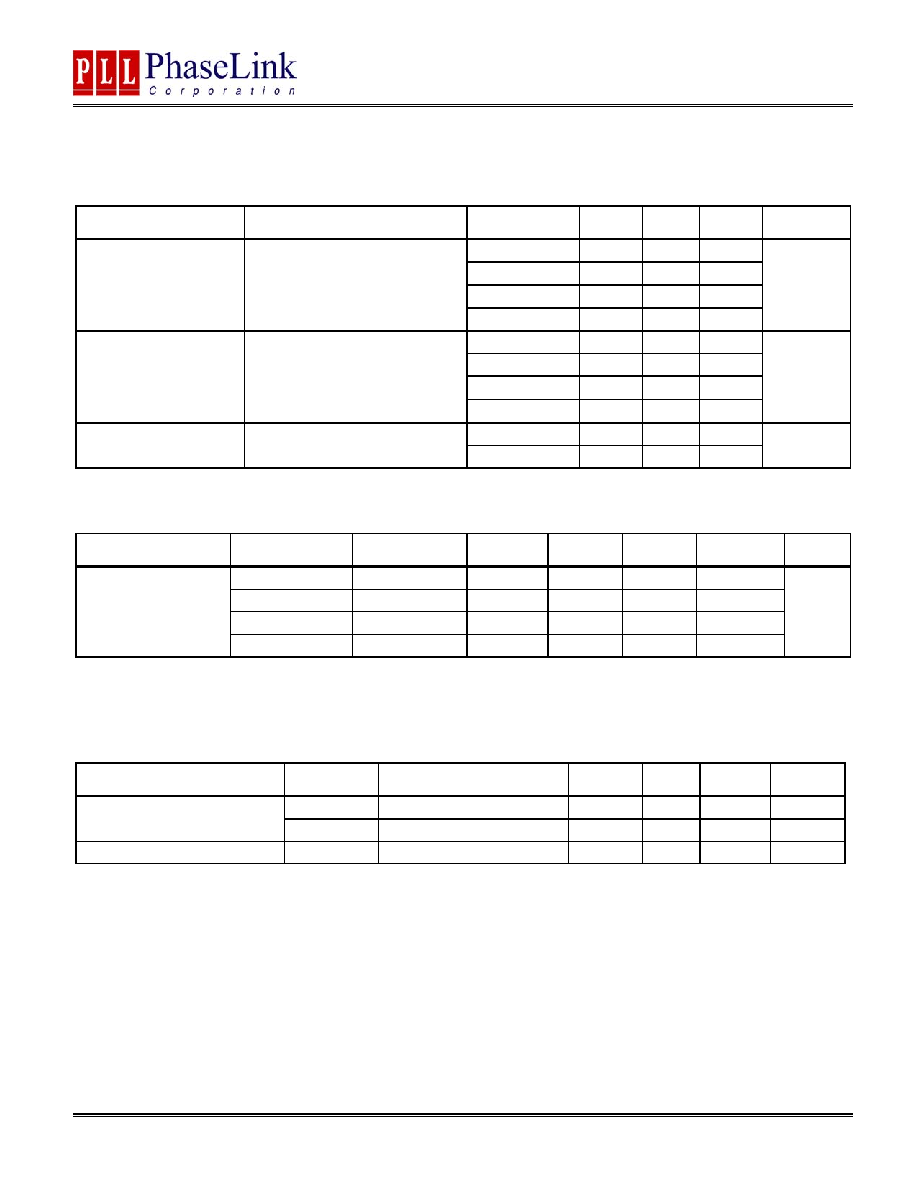
5. Jitter Specifications
PARAMETERS CONDITIONS
FREQUENCY MIN. TYP. MAX. UNITS
19.44MHz 2.2
77.76MHz 4.5
155.52MHz 4.5
Period jitter RMS
With capacitive decoupling be-
tween VDD and GND.
Over 10,000 cycles.
622.08MHz 5.0
ps
19.44MHz 17
77.76MHz 25
155.52MHz 27
Period jitter Peak-to-
Peak
1
With capacitive decoupling be-
tween VDD and GND.
Over 10,000 cycles.
622.08MHz 35
ps
155.52MHz 2.5 4
Integrated jitter RMS
2
Integrated 12 kHz to 20 MHz
622.08MHz 2.5 4
ps
6. Phase Noise Specifications
PARAMETERS FREQUENCY @10Hz
@100Hz @1kHz @10kHz @100kHz UNITS
19.44MHz -80 -108
-132
-142
-150
77.76MHz -72 -103
-122
-130
-125
155.52MHz -65 -95
-120
-125
-121
Phase Noise relative
to carrier
(typical)
622.08MHz -55 -85
-109
-115
-110
dBc/Hz
Note: Phase Noise measured at VCON = 0V
7. CMOS Electrical Characteristics
PARAMETERS SYMBOL CONDITIONS MIN.
TYP.
MAX.
UNITS
I
OH
V
OH
= V
DD
-0.4V, V
DD
=3.3V 10 mA
Output drive current
I
OL
V
OL
= 0.4V, V
DD
= 3.3V
10
mA
Output Clock Rise/Fall Time
0.3V ~ 3.0V with 15 pF load
2.4
ns