
P521-23
Low Phase Noise PECL VCXO (100MHz to 200MHz)
47745 Fremont Blvd., Fremont, California 94538 TEL (510) 492-0990 FAX (510) 492-0991 [www.phaselink.com] Rev 7/28/04 Page 2
PAD ASSIGNMENT AND DESCRIPTION
Pin #
Name
Description
1 OSCOFFSEL
Oscillator Off Selection input pad. When low, turns off the oscillator when output is disabled.
When high (default), oscillator running when output is disabled.
Internal pull-up
2
GNDOSC
GND connection for oscillator circuitry.
3 VCON
Control Voltage input. Use this pin to change the output frequency by varying the applied
Control Voltage.
4 XIN
Crystal oscillator input pin.
5 XOUT
Crystal oscillator output pin.
6 OECTRL
OE input pad. See table on page 1.
7
DNC
Do Not Connect.
8 GND
Ground
connection.
9 GND
Ground
connection.
10 Q
PECL
Output.
11 QBAR
PECL
complementary
output.
12 VDDBUF
VDD connection for output buffer circuitry.
VDDBUF should be separately decoupled from other VDDs whenever possible.
13 VDDANA
VDD connection for analog circuitry.
VDDANA should be separately decoupled from other VDDs whenever possible.
14
OESEL
Selector input to choose the OE control logic. See table on page 1.
15
BUFZSEL
Output impedance selector
16 VDDOSC
VDD connection for oscillator circuitry.
VDDOSC should be separately decoupled from other VDDs whenever possible.

P521-23
Low Phase Noise PECL VCXO (100MHz to 200MHz)
47745 Fremont Blvd., Fremont, California 94538 TEL (510) 492-0990 FAX (510) 492-0991 [www.phaselink.com] Rev 7/28/04 Page 3
ELECTRICAL SPECIFICATIONS
1. Absolute Maximum Ratings
PARAMETERS SYMBOL
MIN.
MAX.
UNITS
Supply Voltage
V
DD
4.6 V
Input Voltage, dc
V
I
V
SS
-0.5 V
DD
+0.5 V
Output Voltage, dc
V
O
V
SS
-0.5 V
DD
+0.5 V
Storage Temperature
T
S
-65 150
�C
Ambient Operating Temperature
T
A
0 70
�C
Junction Temperature
T
J
125
�C
Lead Temperature (soldering, 10s)
260
�C
Input Static Discharge Voltage Protection
2
kV
Exposure of the device under conditions beyond the limits specified by Maximum Ratings for extended periods may cause permanent damage to the
device and affect product reliability. These conditions represent a stress rating only, and functional operations of the device at these or any other
conditions above the operational limits noted in this specification is not implied.
2. Crystal Specifications
PARAMETERS SYMBOL CONDITIONS MIN.
TYP.
MAX.
UNITS
Crystal Resonator Frequency
F
XIN
Parallel Fundamental Mode
100
200
MHz
Crystal Loading Rating
C
L (xtal)
VCON
=
1.65V
5.0
pF
Interelectrode Capacitance
C
0
3.5
pF
Crystal Pullability
C
0
/C
1 (xtal)
AT cut
250 -
Recommended ESR
R
E
AT cut
30
3. Voltage Control Crystal Oscillator
PARAMETERS SYMBOL CONDITIONS MIN.
TYP.
MAX.
UNITS
VCXO Stabilization Time *
T
VCXOSTB
From
power
valid 10
ms
VCXO Tuning Range
XTAL C
0
/C
1
< 250
250*
ppm
CLK output pullability
VCON = 1.65V � 1.65V
at room temperature
�125*
ppm
On-chip Varicaps control range
VCON = 0 to 3.3V
3.3 � 8.8*
pF
Linearity
5*
%
VCXO Tuning Characteristic
70
ppm/V
VCON input impedance
2000
k
VCON modulation BW
0V
VCON 3.3V, -3dB
25
kHz
Note: Parameters denoted with an asterisk (*) represent nominal characterization data and are not production tested to any specific limits.

P521-23
Low Phase Noise PECL VCXO (100MHz to 200MHz)
47745 Fremont Blvd., Fremont, California 94538 TEL (510) 492-0990 FAX (510) 492-0991 [www.phaselink.com] Rev 7/28/04 Page 4
4. General Electrical Specifications
PARAMETERS SYMBOL CONDITIONS MIN.
TYP.
MAX.
UNITS
Supply Current (Loaded Outputs)
I
DD
at 3.3V @ 155MHz
55
mA
Oscillator
off
10 ms
Output valid after OE enabled
Oscillator
on
50 ns
Operating Voltage
V
DD
2.25
3.63
V
Output Clock Duty Cycle
@ Vdd � 1.3V (PECL)
45
50
55
%
Short Circuit Current
�50
mA
5. Jitter specifications
PARAMETERS CONDITIONS
MIN.
TYP.
MAX.
UNITS
Period jitter RMS at 155MHz
2.5
Period jitter peak-to-peak at 155MHz
At 155.52MHz, with capacitive
decoupling between VDD and GND.
Over 10,000 cycles
18.5
20
ps
Accumulated jitter RMS at 155MHz
2.5
Accumulated jitter peak-to-peak at 155MHz
At 155.52MHz, with capacitive
decoupling between VDD and GND.
Over 1,000,000 cycles.
24
27
ps
Random Jitter
"RJ" measured on Wavecrest SIA 3000
2.5
ps
Integrated jitter RMS at 155MHz
Integrated 12 kHz to 20 MHz
0.25
0.35 ps
Measured on Wavecrest SIA 3000
6. Phase noise specifications
PARAMETERS FREQUENCY 10Hz
100Hz 1kHz 10kHz
100kHz
1MHz
UNITS
Phase Noise
relative to carrier
155.52MHz -75 -100 -125 -140 -145 -150
dBc/Hz
Note: Phase Noise measured at VCON = 0V
P521-23
Low Phase Noise PECL VCXO (100MHz to 200MHz)
47745 Fremont Blvd., Fremont, California 94538 TEL (510) 492-0990 FAX (510) 492-0991 [www.phaselink.com] Rev 7/28/04 Page 5
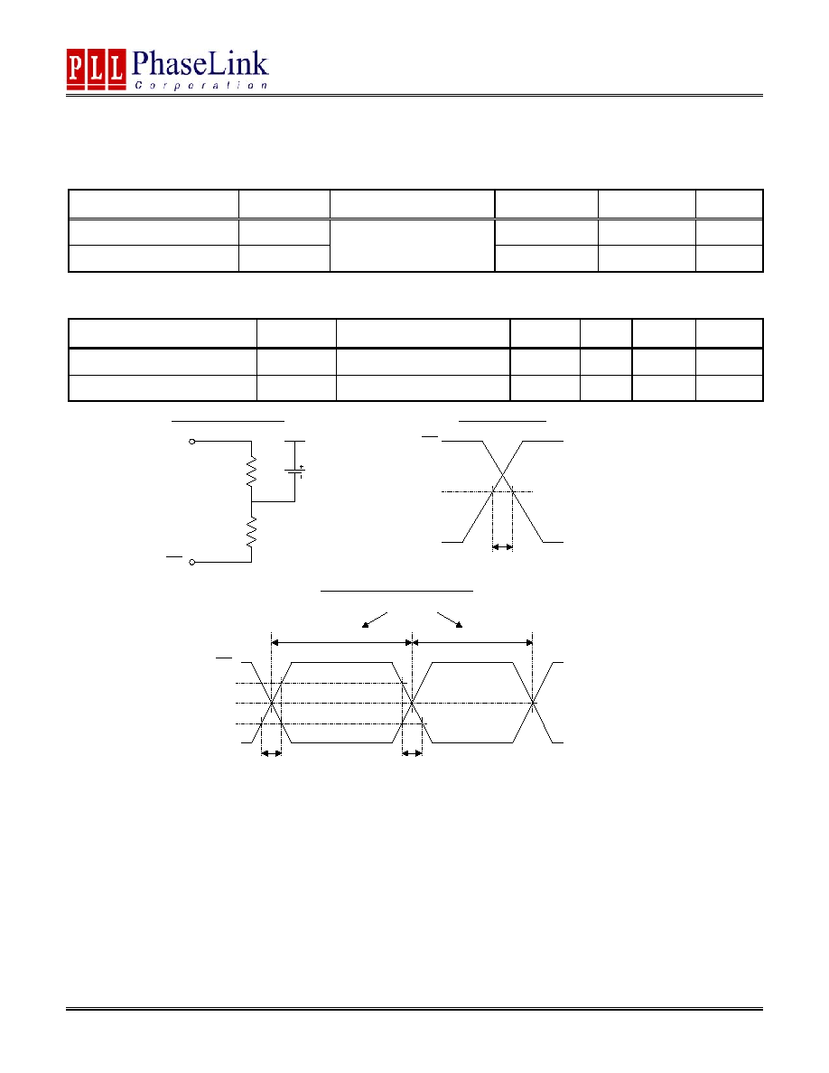
7. PECL Electrical Characteristics
PARAMETERS SYMBOL CONDITIONS
MIN. MAX.
UNITS
Output High Voltage
V
OH
V
DD
� 1.025
V
Output Low Voltage
V
OL
R
L
= 50
to (V
DD
� 2V)
(see figure)
V
DD
� 1.620
V
8. PECL Switching Characteristics
PARAMETERS SYMBOL CONDITIONS MIN.
TYP.
MAX.
UNITS
Clock Rise Time
t
r
@20/80% - PECL
0.6
1.5
ns
Clock Fall Time
t
f
@80/20% - PECL
0.5
1.5
ns
OUT
OUT
50
50
PECL Levels Test Circuit
PECL Transistion Time Waveform
OUT
OUT
50%
20%
80%
t
R
t
F
VDD
DUTY CYCLE
45 - 55%
55 - 45%
50%
OUT
OUT
t
SKEW
PECL Output Skew
2.0V

P521-23
Low Phase Noise PECL VCXO (100MHz to 200MHz)
47745 Fremont Blvd., Fremont, California 94538 TEL (510) 492-0990 FAX (510) 492-0991 [www.phaselink.com] Rev 7/28/04 Page 6
PACKAGE INFORMATION
ORDERING INFORMATION
PhaseLink Corporation, reserves the right to make changes in its products or specifications, or both at any time without notice. The information
furnished by Phaselink is believed to be accurate and reliable. However, PhaseLink makes no guarantee or warranty concerning the accuracy of said
information and shall not be responsible for any loss or damage of whatever nature resulting from the use of, or reliance upon this product.
LIFE SUPPORT POLICY: PhaseLink's products are not authorized for use as critical components in life support devices or systems
without the express written approval of the President of PhaseLink Corporation.
PART NUMBER
The order number for this device is a combination of the following:
Device number, Package type and Operating temperature range
P521-23 D C
Order Number
Marking
Package Option
P521-23DC P521-23DC
Die � Waffle Pack
P521-23OC-R
P521-23
OC
TSSOP � Tape and Reel
P521-23OC
P521-23 OC TSSOP � Tube
PART NUMBER
TEMPERATURE
C=COMMERCIAL
C
L
A
16 PIN Narrow SOIC, TSSOP ( mm )
SOIC
TSSOP
Symbol
Min.
Max.
Min.
Max.
A
1.35
1.75
-
1.20
A1
0.10
0.25
0.05
0.15
B
0.33
0.51
0.19
0.30
C
0.19
0.25
0.09
0.20
D
9.80
10.00
4.90
5.10
E
3.80
4.00
4.30
4.50
H
5.80
6.20
6.40 BSC
L
0.40
1.27
0.45
0.75
e
1.27 BSC
0.65 BSC
E
H
D
A1
e
B
PACKAGE TYPE
D=Die
O=TSSOP