 | –≠–ª–µ–∫—Ç—Ä–æ–Ω–Ω—ã–π –∫–æ–º–ø–æ–Ω–µ–Ω—Ç: P602-89SC | –°–∫–∞—á–∞—Ç—å:  PDF PDF  ZIP ZIP |

PLL602-89
12-27 MHz XO IC with 1 Pair of LVDS and 1 CMOS Outputs
47745 Fremont Blvd., Fremont, California 94538 Tel (510) 492-0990 Fax (510) 492-0991 www.phaselink.com Rev 09/03/04 Page 1
FEATURES
∑ Low jitter XO for the 12MHz to 27MHz range.
∑ Integrated crystal load capacitor: no external
load capacitor required.
∑ 1 pair of LVDS outputs and 1 CMOS output.
∑ 12-27 MHz fundamental crystal input.
∑ Low jitter (RMS): 2.5 ps period jitter (1 sigma).
∑ 2.5V to 3.3V operation.
∑ Available in 8-Pin SOIC package.
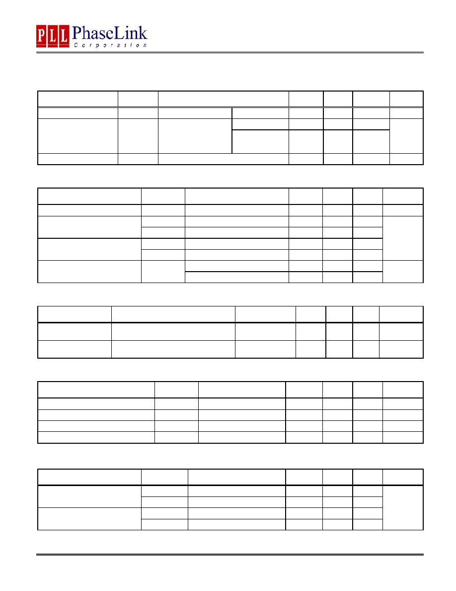
PIN CONFIGURATION
(Top View)
DESCRIPTION
The PLL602-89 is a high performance multiple output XO IC chip. It provides 1 pair of LVDS and 1 CMOS outputs.
The chip combines a crystal oscillator (XO) with a multiple-output buffer. It accepts a low cost fundamental parallel
resonant mode crystal from 12MHz to 27MHz, which is reproduced at the outputs. The very low jitter (2.5 ps RMS
period jitter) makes this chip ideal for data and telecommunication applications.
BLOCK DIAGRAM
PLL
6
02-
8
9
1
2
3
4
5
6
7
8
VDD
XIN
XOUT
GND
CMOS_CLK
LVDS_CLK
GND
LVDSBAR_CLK
XOUT
LVDS_CLK
XIN
CMOS_CLK
Oscillator
Amplifier
LVDSBAR_CLK
(8 pin SOIC)

PLL602-89
12-27 MHz XO IC with 1 Pair of LVDS and 1 CMOS Outputs
47745 Fremont Blvd., Fremont, California 94538 Tel (510) 492-0990 Fax (510) 492-0991 www.phaselink.com Rev 09/03/04 Page 2
PIN DESCRIPTION
Name
Pin
Number
Type Description
VDD 1
P
Power
Supply.
XIN 2
I
Crystal input. This is the input of the crystal oscillator circuitry. The crystal
should be mounted as close to the IC as possible, with minimum parasitic
capacitance.
XOUT 3
I
Crystal output. This is the output of the crystal oscillator circuitry. The crystal
should be mounted as close to the IC as possible, with minimum parasitic
capacitance.
GND 4,5
P
Ground.
LVDS_CLK 6 O
LVDS
output.
LVDSBAR_CLK 7 O
LVDS
complementary
output.
CMOS_CLK 8 O
CMOS
output.
ELECTRICAL SPECIFICATIONS
1. Absolute Maximum Ratings
PARAMETERS SYMBOL
MIN.
MAX.
UNITS
Supply Voltage
V
DD
4.6 V
Input Voltage, dc
V
I
-0.5
V
DD
+0.5 V
Output Voltage, dc
V
O
-0.5
V
DD
+0.5 V
Storage Temperature
T
S
-65 150
∞C
Ambient Operating Temperature*
T
A
-40 85
∞C
Junction Temperature
T
J
125
∞C
Lead Temperature (soldering, 10s)
260
∞C
ESD Protection, Human Body Model
2
kV
Exposure of the device under conditions beyond the limits specified by Maximum Ratings for extended periods may cause permanent damage to the
device and affect product reliability. These conditions represent a stress rating only, and functional operations of the device at these or any other con-
ditions above the operational limits noted in this specification is not implied.
* Note: Operating Temperature is guaranteed by design for all parts (COMMERCIAL and INDUSTRIAL), but tested for COMMERCIAL grade only.
2. Crystal Specifications
PARAMETERS SYMBOL CONDITIONS MIN.
TYP.
MAX.
UNITS
Crystal Resonator Frequency
F
XIN
Parallel Fundamental Mode
12
27
MHz
Crystal Loading Rating
C
L (xtal)
21.5
pF
Recommended ESR
R
E
30
PLL602-89
12-27 MHz XO IC with 1 Pair of LVDS and 1 CMOS Outputs
47745 Fremont Blvd., Fremont, California 94538 Tel (510) 492-0990 Fax (510) 492-0991 www.phaselink.com Rev 09/03/04 Page 3
3. General Electrical Specifications
PARAMETERS SYMBOL
CONDITIONS
MIN. TYP. MAX. UNITS
Operating Voltage
V
DD
2.25
3.63
V
Fout = 12 MHz
15
20
Supply Current, Dy-
namic (with Loaded
Outputs)
I
DD
CMOS outputs
loaded with 15pF,
LVDS outputs loaded
with 100
Fout = 25 MHz
20
25
mA
Short Circuit Current
±50
mA
4. AC Electrical Specifications
PARAMETERS SYMBOL CONDITIONS MIN.
TYP.
MAX.
UNITS
Input Crystal Frequency
12
27
MHz
t
r
0.8V ~ 2.0V with 10 pF load
1.5
Output Clock Rise Time
t
r
0.3V ~ 3.0V with 15 pF load
2
5
t
f
2.0V ~ 0.8V with 10 pF load
1.5
Output Clock Fall Time
t
f
3.0V ~ 0.3V with 15pF load
2
5
ns
Measured @ 1.25 V (LVDS)
45
50
55
Output Clock Duty Cycle
Measured @ 50% V
DD
(CMOS)
45
50
55
%
5. Jitter Specifications
PARAMETERS CONDITIONS FREQUENCY MIN. TYP.
MAX. UNITS
Period jitter RMS
With capacitive decoupling between
VDD and GND.
25MHz
2.5
4
ps
Peak to Peak jitter
With capacitive decoupling between
VDD and GND. Over 10,000 cycles.
25MHz
18
30
ps
6. CMOS Output Electrical Specifications
PARAMETERS SYMBOL
CONDITIONS
MIN.
TYP.
MAX.
UNITS
Output High Voltage
V
OH
I
OH
= -12mA
2.4
V
Output Low Voltage
V
OL
I
OL
= 12mA
0.4
V
Output High Voltage at CMOS level
V
OHC
I
OH
= -4mA
V
DD
≠ 0.4
V
Output drive current
At TTL level
10
mA
7. CMOS Switching Characteristics
PARAMETERS SYMBOL CONDITIONS MIN.
TYP.
MAX.
UNITS
0.8V ~ 2.0V with 10 pF load
1.15
Output Clock Rise/Fall Time
(Standard Drive)
0.3V ~ 3.0V with 15 pF load
2.4
0.8V ~ 2.0V with 10 pF load
0.5
Output Clock Rise/Fall Time
(High Drive)
0.3V ~ 3.0V with 15 pF load
1.5
ns

PLL602-89
12-27 MHz XO IC with 1 Pair of LVDS and 1 CMOS Outputs
47745 Fremont Blvd., Fremont, California 94538 Tel (510) 492-0990 Fax (510) 492-0991 www.phaselink.com Rev 09/03/04 Page 4
8. LVDS Electrical Characteristics
PARAMETERS SYMBOL
CONDITIONS
MIN.
TYP.
MAX.
UNITS
Output Differential Voltage
V
OD
247
355
454
mV
V
DD
Magnitude Change
V
OD
-50 50 mV
Output High Voltage
V
OH
1.4
1.6
V
Output Low Voltage
V
OL
0.9
1.1
V
Offset Voltage
V
OS
1.125
1.2
1.375
V
Offset Magnitude Change
V
OS
R
L
= 100
(see figure)
0 3 25 mV
Power-off Leakage
I
OXD
V
out
= V
DD
or GND
V
DD
= 0V
±1
±10
uA
Output Short Circuit Current
I
OSD
-5.7 -8
mA
9. LVDS Switching Characteristics
PARAMETERS SYMBOL
CONDITIONS
MIN.
TYP.
MAX.
UNITS
Differential Clock Rise Time
t
r
0.2 0.7 1.0 ns
Differential Clock Fall Time
t
f
R
L
= 100
C
L
= 10 pF
(see figure)
0.2 0.7 1.0 ns
OUT
OUT
V
OD
V
OS
50
50
OUT
V
DIFF
R
L
= 100
C
L
= 10pF
C
L
= 10pF
LVDS Switching Test Circuit
LVDS Levels Test Circuit
LVDS Transistion Time Waveform
OUT
OUT
OUT
0V (Differential)
0V
20%
80%
20%
80%
t
R
t
F
V
DIFF
PLL602-89
12-27 MHz XO IC with 1 Pair of LVDS and 1 CMOS Outputs
47745 Fremont Blvd., Fremont, California 94538 Tel (510) 492-0990 Fax (510) 492-0991 www.phaselink.com Rev 09/03/04 Page 5
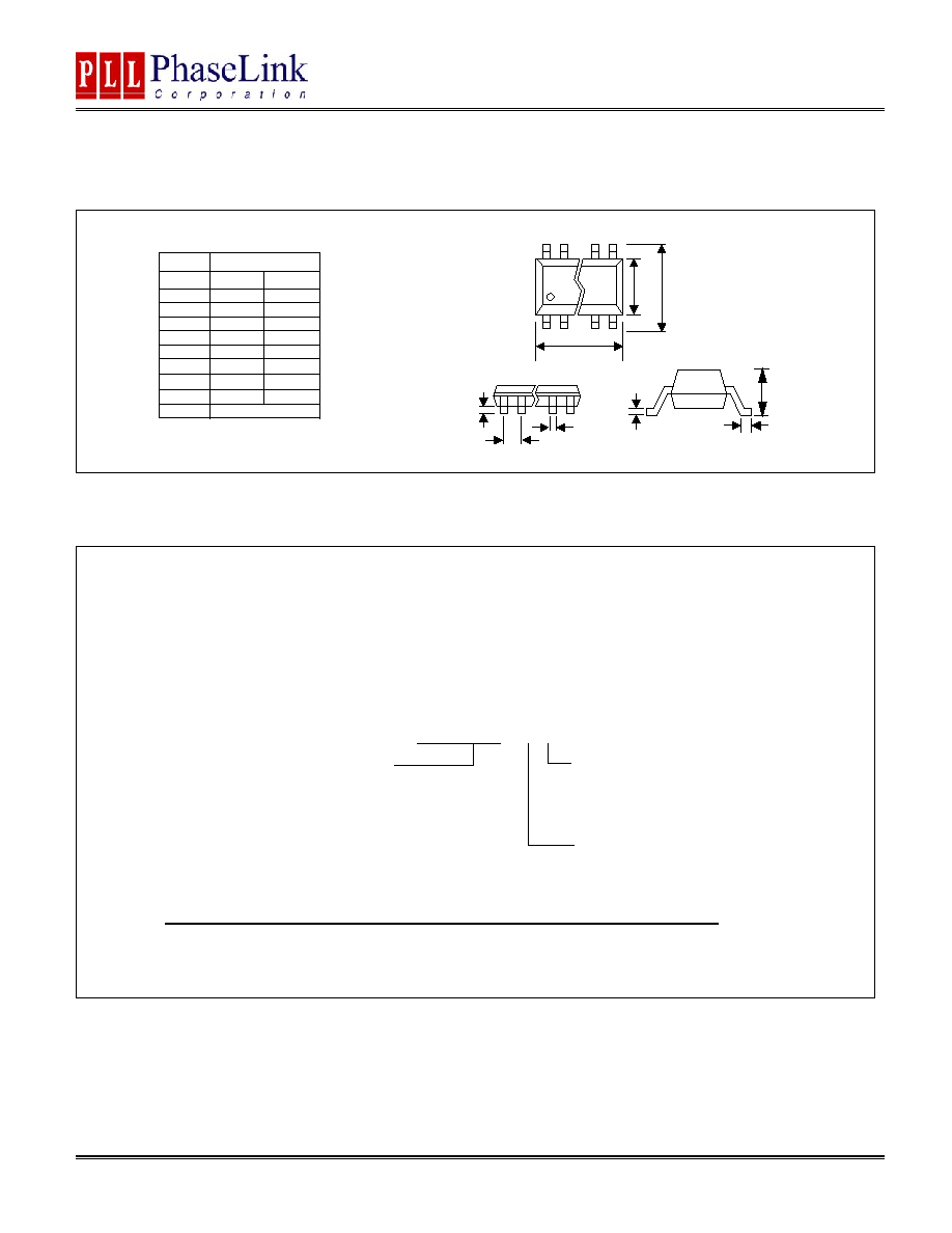
PACKAGE INFORMATION
ORDERING INFORMATION
PhaseLink Corporation, reserves the right to make changes in its products or specifications, or both at any time without notice. The information fur-
nished by Phaselink is believed to be accurate and reliable. However, PhaseLink makes no guarantee or warranty concerning the accuracy of said
information and shall not be responsible for any loss or damage of whatever nature resulting from the use of, or reliance upon this product.
LIFE SUPPORT POLICY: PhaseLink's products are not authorized for use as critical components in life support devices or systems without the ex-
press written approval of the President of PhaseLink Corporation.
For part ordering, please contact our Sales Department:
47745 Fremont Blvd., Fremont, CA 94538, USA
Tel: (510) 492-0990 Fax: (510) 492-0991
PART NUMBER
The order number for this device is a combination of the following:
Device number, Package type and Operating temperature range
PLL602-89 S C
Order Number
Marking
Package Option
PLL602-89SC-R P602-89SC SOIC - Tape and Reel
PLL602-89SC
P602-89SC SO
IC
- Tube
PART NUMBER
TEMPERATURE
C=COMMERCIAL
I=INDUSTRIAL
PACKAGE TYPE
S=SOIC
C
L
A
8 PIN SOIC (mm )
Narrow SOIC
Symbol
Min.
Max.
A
1.47
1.73
A
1
0.10
0.25
B
0.33
0.51
C
0.19
0.25
D
4.80
4.95
E
3.80
4.00
H
5.80
6.20
L
0.38
1.27
e
1.27 BSC
E
H
D
A
1
e
B