PLL620-28/-29
Low Phase Noise VCXO (for 100-200MHz Fund Xtal)
47745 Fremont Blvd., Fremont, California 94538 Tel (510) 492-0990 Fax (510) 492-0991
www.phaselink.com Rev 07/08/05 Page 1
FEATURES
∑ 100MHz to 200MHz Fundamental Mode Crystal.
∑ Output range: 100 ≠ 200MHz (no PLL).
∑ Low Injection Power for crystal 50uW.
∑ Sub 0.5pS RMS phase jitter ( 12kHz to 20MHz ).
∑ PECL (PLL620-28) or LVDS output (PLL620-29).
∑ Supports 2.5V or 3.3V-Power Supply.
∑ Available in 16-Pin TSSOP.
DESCRIPTION
The PLL620-28/-29 family of XO ICs is specifically
designed to work with high frequency fundamental
and third overtone crystals. They achieve very low
current into the crystal, resulting in better stability.
Their very low jitter makes them ideal for the most
demanding timing requirements.
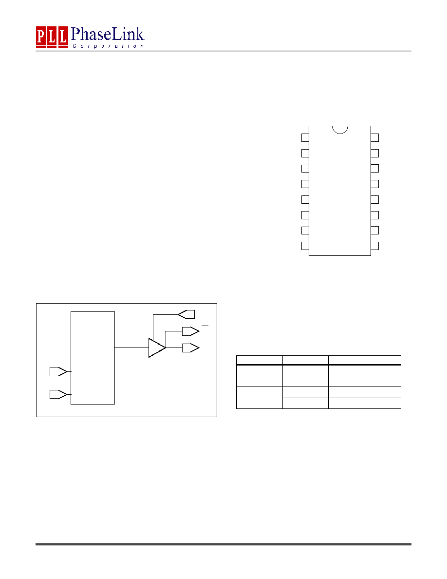
BLOCK DIAGRAM
PIN CONFIGURATION
(Top View)
OUTPUT ENABLE LOGICAL LEVELS
Part #
OE
State
0 (Default)
Output enabled
PLL620-28
1
Tri-state
0
Tri-state
PLL620-29
1 (Default)
Output enabled
OE input: Logical states defined by PECL levels for PLL620-28
Logical states defined by CMOS levels for PLL620-29
XIN
XOUT
OE
Q
PLL620-28/-29
Q
Oscillator
Amplifier
PLL620-28/-29
Low Phase Noise VCXO (for 100-200MHz Fund Xtal)
47745 Fremont Blvd., Fremont, California 94538 Tel (510) 492-0990 Fax (510) 492-0991
www.phaselink.com Rev 07/08/05 Page 2
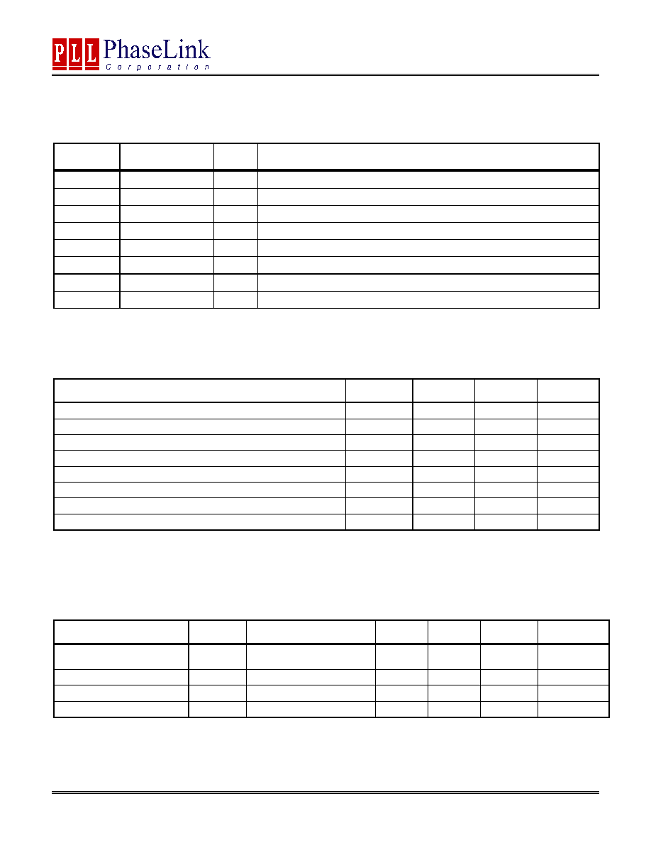
PIN DESCRIPTIONS
Name
Pin number
Type
Description
XIN
2
I
Crystal input. See Crystal Specifications on page 2.
XOUT
3
I
Crystal output. See Crystal Specifications on page 2.
OE
6
I
Output enable pin. See Output Enable Logic Levels on page 1.
GND
8, 9, 10, 14
P
Ground.
CLKT
11
O
True output PECL (PLL620-28) or LVDS (PLL620-29)
CLKC
13
O
Complementary output PECL (PLL620-28) or LVDS (PLL620-29).
DNC
4, 5, 7, 15, 16
-
DO Not connect.
VDD
1, 12
P
Power supply.
ELECTRICAL SPECIFICATIONS
1. Absolute Maximum Ratings
PARAMETERS
SYMBOL
MIN.
MAX.
UNITS
Supply Voltage
V
DD
4.6
V
Input Voltage, dc
V
I
-0.5
V
DD
+0.5
V
Output Voltage, dc
V
O
-0.5
V
DD
+0.5
V
Storage Temperature
T
S
-65
150
∞C
Ambient Operating Temperature*
T
A
-40
85
∞C
Junction Temperature
T
J
125
∞C
Lead Temperature (soldering, 10s)
260
∞C
ESD Protection, Human Body Model
2
kV
Exposure of the device under conditions beyond the limits specified by Maximum Ratings for extended periods may cause permanent damage to the
device and affect product reliability. These conditions represent a stress rating only, and functional operations of the device at these or any other
conditions above the operational limits noted in this specification is not implied.
*
Note: Operating Temperature is guaranteed by design for all parts (COMMERCIAL and INDUSTRIAL), but tested for COMMERCIAL grade only.
2. Crystal Specifications
PARAMETERS
SYMBOL
CONDITIONS
MIN.
TYP.
MAX.
UNITS
Built-in Load Capacitance
C
L
IC only, no PCB
capacitance included.
4
pF
Shunt Capacitance
C
0
2
pF
Oscillation Frequency
OF
Fund. Or 3
rd
Overtone
100
200
MHz
Recommended ESR
R
E
30
PLL620-28/-29
Low Phase Noise VCXO (for 100-200MHz Fund Xtal)
47745 Fremont Blvd., Fremont, California 94538 Tel (510) 492-0990 Fax (510) 492-0991
www.phaselink.com Rev 07/08/05 Page 3
3. General Electrical Specifications
PARAMETERS
SYMBOL
CONDITIONS
MIN.
TYP.
MAX.
UNITS
Supply Current (Loaded
Outputs)
I
DD
PECL/LVDS
100/80
mA
Operating Voltage
V
DD
2.97
3.63
V
Output Clock Duty Cycle
@ 1.25V (LVDS)
@ V
DD
≠ 1.3V (PECL)
45
45
50
50
55
55
%
Short Circuit Current
±50
mA
4. Jitter Specifications
PARAMETERS
CONDITIONS
MIN.
TYP.
MAX.
UNITS
Period jitter RMS
2.5
Period jitter peak-to-peak
At 155.52MHz, with capacitive decoupling
between VDD and GND.
18.5
ps
Accumulated jitter RMS
2.5
Accumulated jitter peak-to-peak
At 155.52MHz, with capacitive decoupling
between VDD and GND. Over 10,000
cycles.
24
ps
Integrated jitter RMS at 155MHz
Integrated 12 kHz to 20 MHz
0.3
ps
5. Phase Noise Specifications
PARAMETERS
FREQUENCY @10Hz @100Hz @1kHz @10kHz @100kHz UNITS
Phase Noise relative to carrier
155.52MHz
-80
-110
-125
-143
-145
dBc/Hz
PLL620-28/-29
Low Phase Noise VCXO (for 100-200MHz Fund Xtal)
47745 Fremont Blvd., Fremont, California 94538 Tel (510) 492-0990 Fax (510) 492-0991
www.phaselink.com Rev 07/08/05 Page 4
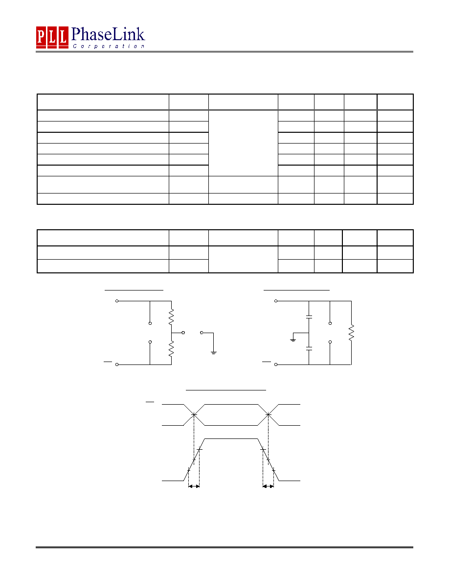
6. LVDS Electrical Characteristics
PARAMETERS
SYMBOL
CONDITIONS
MIN.
TYP.
MAX.
UNITS
Output Differential Voltage
V
OD
247
355
454
mV
V
DD
Magnitude Change
V
OD
-50
50
mV
Output High Voltage
V
OH
1.4
1.6
V
Output Low Voltage
V
OL
0.9
1.1
V
Offset Voltage
V
OS
1.125
1.2
1.375
V
Offset Magnitude Change
V
OS
R
L
= 100
(see figure)
0
3
25
mV
Power-off Leakage
I
OXD
V
out
= V
DD
or GND
V
DD
= 0V
±1
±10
uA
Output Short Circuit Current
I
OSD
-5.7
-8
mA
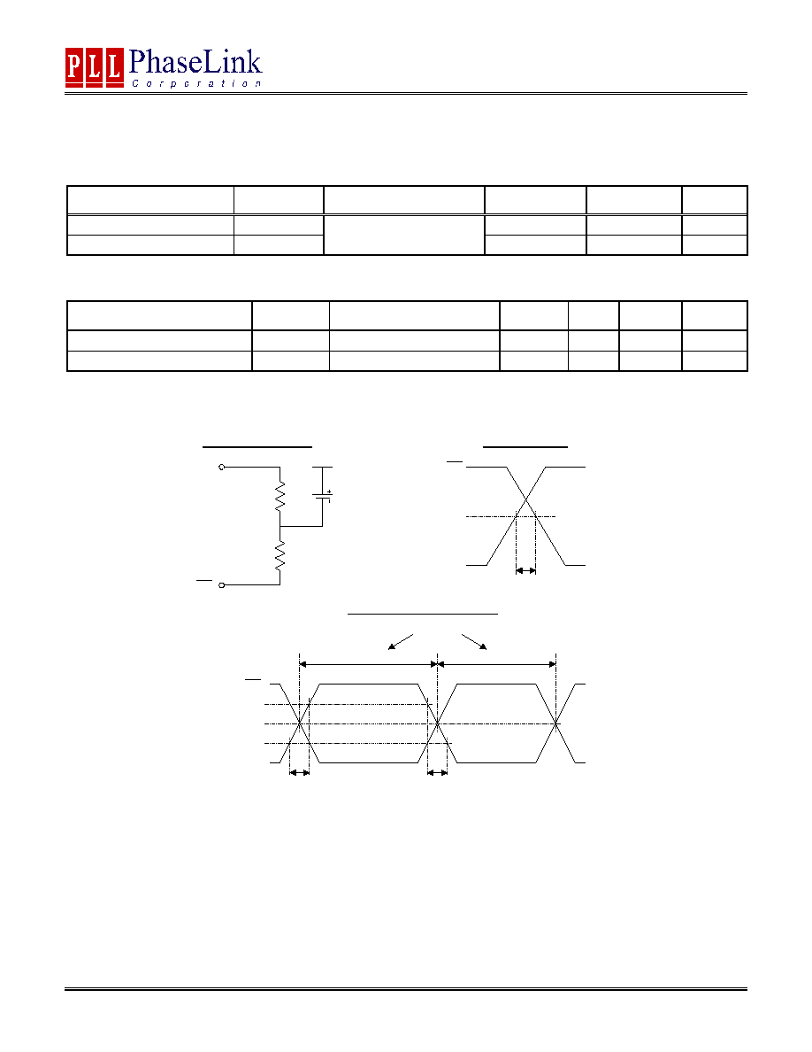
7. LVDS Switching Characteristics
PARAMETERS
SYMBOL
CONDITIONS
MIN.
TYP.
MAX.
UNITS
Differential Clock Rise Time
t
r
0.2
0.7
1.0
ns
Differential Clock Fall Time
t
f
R
L
= 100
C
L
= 10 pF
(see figure)
0.2
0.7
1.0
ns
OUT
OUT
V
OD
V
OS
50
50
OUT
V
DIFF
R
L
= 100
C
L
= 10pF
C
L
= 10pF
LVDS Switching Test Circuit
LVDS Levels Test Circuit
LVDS Transistion Time Waveform
OUT
OUT
OUT
0V (Differential)
0V
20%
80%
20%
80%
t
R
t
F
V
DIFF
PLL620-28/-29
Low Phase Noise VCXO (for 100-200MHz Fund Xtal)
47745 Fremont Blvd., Fremont, California 94538 Tel (510) 492-0990 Fax (510) 492-0991
www.phaselink.com Rev 07/08/05 Page 5
8. PECL Electrical Characteristics
PARAMETERS
SYMBOL
CONDITIONS
MIN.
MAX.
UNITS
Output High Voltage
V
OH
V
DD
≠ 1.025
V
Output Low Voltage
V
OL
R
L
= 50
to (V
DD
≠ 2V)
(see figure)
V
DD
≠ 1.620
V
9. PECL Switching Characteristics
PARAMETERS
SYMBOL
CONDITIONS
MIN.
TYP.
MAX.
UNITS
Clock Rise Time
t
r
@20/80% - PECL
0.6
1.5
ns
Clock Fall Time
t
f
@80/20% - PECL
0.5
1.5
ns
OUT
OUT
50
50
PECL Levels Test Circuit
PECL Transistion Time Waveform
OUT
OUT
50%
20%
80%
t
R
t
F
VDD
DUTY CYCLE
45 - 55%
55 - 45%
50%
OUT
OUT
t
SKEW
PECL Output Skew
2.0V
PLL620-28/-29
Low Phase Noise VCXO (for 100-200MHz Fund Xtal)
47745 Fremont Blvd., Fremont, California 94538 Tel (510) 492-0990 Fax (510) 492-0991
www.phaselink.com Rev 07/08/05 Page 6
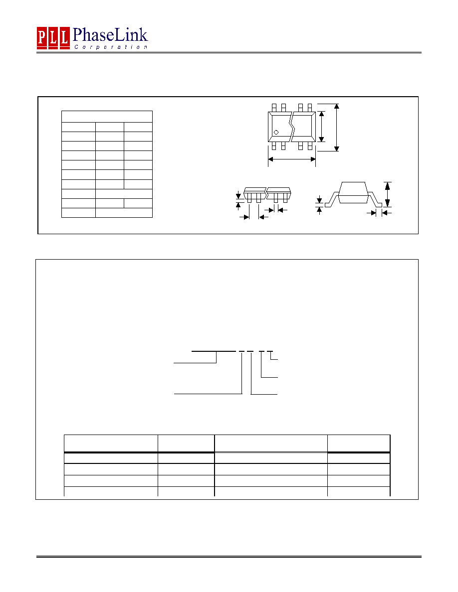
PACKAGE INFORMATION
C
L
A
E
H
D
A1
e
B
16 PIN TSSOP ( mm )
Symbol
Min.
Max.
A
-
1.20
A1
0.05
0.15
B
0.19
0.30
C
0.09
0.20
D
4.90
5.10
E
4.30
4.50
H
6.40 BSC
L
0.45
0.75
e
0.65 BSC
ORDERING INFORMATION
PhaseLink Corporation, reserves the right to make changes in its products or specifications, or both at any time without notice. The information
furnished by Phaselink is believed to be accurate and reliable. However, PhaseLink makes no guarantee or warranty concerning the accuracy of said
information and shall not be responsible for any loss or damage of whatever nature resulting from the use of, or reliance upon this product.
LIFE SUPPORT POLICY: PhaseLink's products are not authorized for use as critical components in life support devices or systems without the
express written approval of the President of PhaseLink Corporation.
For part ordering, please contact our Sales Department:
47745 Fremont Blvd., Fremont, CA 94538, USA
Tel: (510) 492-0990 Fax: (510) 492-0991
PART NUMBER
The order number for this device is a combination of the following:
Device number, Package type and Operating temperature range
PLL620-2X X C L R
Part / Order Number
Marking
Package Option
Temperature
PLL620-2XOC-R
P620-2XOC
TSSOP -Tape and Reel
0 to +70 C
PLL620-2XOC
P620-2XOC
TSSOP≠Tubes
0 to +70 C
PLL620-2XOCL-R
P620-2XOCL
TSSOP-Tape and ReeL (GREEN)
0 to +70 C
PLL620-2XOC
P620-2XOCL
TSSOP≠Tubes (GREEN)
0 to +70 C
PART NUMBER
TEMPERATURE
C=COMMERCIAL,
I=INDUSTRIAL
PACKAGE TYPE
O=TSSOP
NONE=NORMAL PACKAGE
L=GREEN PACKAGE
NONE= TUBE
R=TAPE AND REEL