 | –≠–ª–µ–∫—Ç—Ä–æ–Ω–Ω—ã–π –∫–æ–º–ø–æ–Ω–µ–Ω—Ç: P620-30DC | –°–∫–∞—á–∞—Ç—å:  PDF PDF  ZIP ZIP |
PLL620-30
PECL and LVDS Low Phase Noise XO (32.5 to 130MHz output)
47745 Fremont Blvd., Fremont, California 94538 Tel (510) 492-0990 Fax (510) 492-0991
www.phaselink.com Rev 11/09/04 Page 1
FEATURES
∑ 65MHz to 130MHz Crystal input.
∑ Output range: 32.5MHz ≠ 130MHz (no PLL).
∑ Low Injection Power for crystal, 50uW.
∑ Complementary outputs: PECL or LVDS.
∑ Selectable OE Logic
∑ Supports 2.5V or 3.3V-Power Supply.
∑ Available in die form.
∑ Thickness 10 mil.
DESCRIPTION
The PLL620-30 is a XO IC specifically designed to
drive fundamental or 3
rd
OT crystals from 65MHz to
130MHz, with selectable PECL or LVDS outputs and
OE logic (enable high or enable low). Its design was
optimized to tolerate higher limits of interelectrode
capacitance and bonding capacitance to improve
yield. It achieves very low current into the crystal
resulting in better overall stability.
DIE SPECIFICATIONS
Name
Value
Size
62 x 65 mil
Reverse side
GND
Pad dimensions
80 micron x 80 micron
Thickness
10 mil
BLOCK DIAGRAM
DIE CONFIGURATION
OUTPUT SELECTION AND ENABLE
OUTSEL
(Pad #9)
Selected Output
0
LVDS
1
PECL (default)
OESEL
(Pad #25)
OE_CTRL
(Pad #30)
State
0
Tri-state
0
1
Output enabled (default)
0
Output enabled (default)
1 (default)
1
Tri-state
Pad #9, #25: Bond to GND to set to "0". Internal pull up.
Pad #30: Logical states defined by PECL levels if OESEL is "1"
Logical states defined by CMOS levels if OESEL is "0"
OUTPUT FREQUENCY SELECTOR
S2
Output
0
Input/2
1(Default)*
Input
*Internally set to `Default' through 60K pull-up resistor
18
19
20
21
23
25
7
13
10
26
29
31
Y
X
(0,0)
(1550,1475)
6
2
m
i
l
65 mil
24
22
17
16
15
14
12
11
9
8
6
1
2
3
4
5
27
28
30
G
N
D
G
N
D
G
N
D
G
N
D
G
N
D
G
N
D
B
U
F
G
N
D
B
U
F
OUTSEL^
PECL
LVDS
VDDBUF
VDDBUF
PECLB
LVDSB
N/C
GNDBUF
R
e
s
e
r
v
e
d
R
e
s
e
r
v
e
d
N
/
C
V
D
D
V
D
D
V
D
D
V
D
D
O
E
S
E
L
^
XIN
XOUT
N/C
OE
CTRL
S2^
N/C
R
e
s
e
r
v
e
d
Die ID:
A2020-20A
C502A
XIN
XOUT
OE
Q
PLL620-30
Q
Oscillator
Amplifier

PLL620-30
PECL and LVDS Low Phase Noise XO (32.5 to 130MHz output)
47745 Fremont Blvd., Fremont, California 94538 Tel (510) 492-0990 Fax (510) 492-0991
www.phaselink.com Rev 11/09/04 Page 2
ELECTRICAL SPECIFICATIONS
1. Absolute Maximum Ratings
PARAMETERS
SYMBOL
MIN.
MAX.
UNITS
Supply Voltage
V
DD
4.6
V
Input Voltage, dc
V
I
-0.5
V
DD
+0.5
V
Output Voltage, dc
V
O
-0.5
V
DD
+0.5
V
Storage Temperature
T
S
-65
150
∞C
Ambient Operating Temperature*
T
A
-40
85
∞C
Junction Temperature
T
J
125
∞C
Lead Temperature (soldering, 10s)
260
∞C
ESD Protection, Human Body Model
2
kV
Exposure of the device under conditions beyond the limits specified by Maximum Ratings for extended periods may cause permanent damage to the
device and affect product reliability. These conditions represent a stress rating only, and functional operations of the device at these or any other
conditions above the operational limits noted in this specification is not implied.
*
Note: Operating Temperature is guaranteed by design for all parts (COMMERCIAL and INDUSTRIAL), but tested for COMMERCIAL grade only.
2. Crystal Specifications
3. General Electrical Specifications
PARAMETERS
SYMBOL
CONDITIONS
MIN.
TYP.
MAX.
UNITS
Supply Current (Loaded
Outputs)
I
DD
PECL/LVDS
100/80
mA
Operating Voltage
V
DD
2.97
3.63
V
Output Clock Duty Cycle
@ 1.25V (LVDS)
@ V
DD
≠ 1.3V (PECL)
45
45
50
50
55
55
%
Short Circuit Current
±50
mA
4. Jitter Specifications
PARAMETERS
CONDITIONS
MIN.
TYP.
MAX.
UNITS
Period jitter RMS
77.76MHz
2.5
ps
Period jitter peak-to-peak
77.76MHz
18.5
ps
Integrated jitter RMS
Integrated 12 kHz to 20 MHz at 77.76MHz
0.5
ps
5. Phase Noise Specifications
PARAMETERS
FREQUENCY
@10Hz
@100Hz
@1kHz
@10kHz
@100kHz
UNITS
Phase Noise relative
to carrier
77.76MHz
-75
-95
-125
-145
-155
dBc/Hz
PARAMETERS
SYMBOL
CONDITIONS
MIN.
TYP.
MAX.
UNITS
CX+
2
Built-in Capacitance
CX-
2
Inter-electrode capacitance
C
0
65MHz to 130MHz
(VDD=3.3V)
2.6
pF
Oscillation Frequency
OF
Fund.
65
130
MHz
PLL620-30
PECL and LVDS Low Phase Noise XO (32.5 to 130MHz output)
47745 Fremont Blvd., Fremont, California 94538 Tel (510) 492-0990 Fax (510) 492-0991
www.phaselink.com Rev 11/09/04 Page 3
6. LVDS Electrical Characteristics
PARAMETERS
SYMBOL
CONDITIONS
MIN.
TYP.
MAX.
UNITS
Output Differential Voltage
V
OD
247
355
454
mV
V
DD
Magnitude Change
V
OD
-50
50
mV
Output High Voltage
V
OH
1.4
1.6
V
Output Low Voltage
V
OL
0.9
1.1
V
Offset Voltage
V
OS
1.125
1.2
1.375
V
Offset Magnitude Change
V
OS
R
L
= 100
(see figure)
0
3
25
mV
Power-off Leakage
I
OXD
V
out
= V
DD
or GND
V
DD
= 0V
±1
±10
uA
Output Short Circuit Current
I
OSD
-5.7
-8
mA
7. LVDS Switching Characteristics
PARAMETERS
SYMBOL
CONDITIONS
MIN.
TYP.
MAX.
UNITS
Differential Clock Rise Time
t
r
0.2
0.7
1.0
ns
Differential Clock Fall Time
t
f
R
L
= 100
C
L
= 10 pF
(see figure)
0.2
0.7
1.0
ns
OUT
OUT
V
OD
V
OS
50
50
OUT
V
DIFF
R
L
= 100
C
L
= 10pF
C
L
= 10pF
LVDS Switching Test Circuit
LVDS Levels Test Circuit
LVDS Transistion Time Waveform
OUT
OUT
OUT
0V (Differential)
0V
20%
80%
20%
80%
t
R
t
F
V
DIFF

PLL620-30
PECL and LVDS Low Phase Noise XO (32.5 to 130MHz output)
47745 Fremont Blvd., Fremont, California 94538 Tel (510) 492-0990 Fax (510) 492-0991
www.phaselink.com Rev 11/09/04 Page 4
8. PECL Electrical Characteristics
PARAMETERS
SYMBOL
CONDITIONS
MIN.
MAX.
UNITS
Output High Voltage
V
OH
V
DD
≠ 1.025
V
DD
≠ 0.750
V
Output Low Voltage
V
OL
R
L
= 50
to (V
DD
≠ 2V)
(see figure)
V
DD
≠ 1.900
V
DD
≠ 1.620
V
9. PECL Switching Characteristics
PARAMETERS
SYMBOL
CONDITIONS
MIN.
TYP.
MAX.
UNITS
Clock Rise Time
t
r
@20/80% - PECL
0.3
0.6
1.5
ns
Clock Fall Time
t
f
@80/20% - PECL
0.3
0.5
1.5
ns
OUT
OUT
50
50
PECL Levels Test Circuit
PECL Transistion Time Waveform
OUT
OUT
50%
20%
80%
t
R
t
F
VDD
DUTY CYCLE
45 - 55%
55 - 45%
50%
OUT
OUT
t
SKEW
PECL Output Skew
2.0V

PLL620-30
PECL and LVDS Low Phase Noise XO (32.5 to 130MHz output)
47745 Fremont Blvd., Fremont, California 94538 Tel (510) 492-0990 Fax (510) 492-0991
www.phaselink.com Rev 11/09/04 Page 5
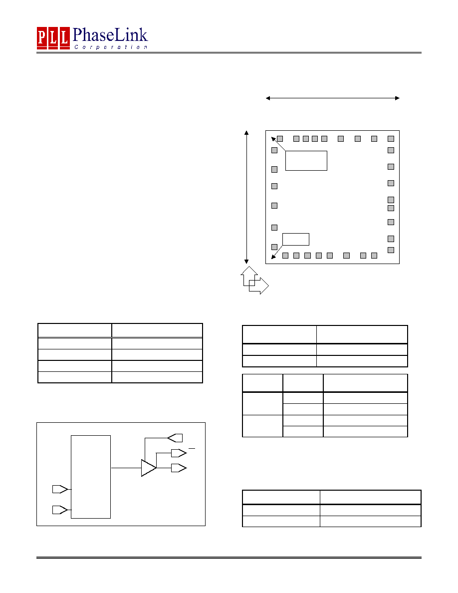
PAD ASSIGNMENT
Pad #
Name
X (µ
µ
µ
µm)
Y (µ
µ
µ
µm)
Description
1
Optional GND
248
109
Optional Ground.
2
Optional GND
361
109
Optional Ground.
3
Optional GND
473
109
Optional Ground.
4
Optional GND
587
109
Optional Ground.
5
GND
702
109
Ground.
6
Reserved
874
109
Reserved for future use.
7
Optional GNDBUF
1042
109
Optional Ground, buffer circuitry.
8
GNDBUF
1171
109
Ground, buffer circuitry.
9
OUTSEL
1400
125
Output type selector. Internal pull up. See Output
Selection and Enable table on page 1. Internal pull
up.
10
LVDS
1400
259
LVDS output.
11
PECL
1400
476
PECL output.
12
VDDBUF
1400
616
Power supply, buffer circuitry.
13
Optional VDDBUF
1400
716
Optional Power supply, buffer circuitry.
14
PECLB
1400
871
Complementary PECL output.
15
LVDSB
1400
1089
Complementary LVDS output.
16
Not connected
1400
1227
Not Connected.
17
GNDBUF
1389
1365
Ground, buffer circuitry.
18
Reserved
1232
1365
Reserved for future use.
19
Reserved
1042
1365
Reserved for future use.
20
Not connected
854
1365
Not Connected.
21
Optional VDD
659
1365
Optional Power supply.
22
Optional VDD
559
1365
Optional Power supply.
23
VDD
459
1365
Power supply.
24
Optional VDD
358
1365
Optional Power supply.
25
OESEL
194
1365
Used to choose between PECL and CMOS OE logic
levels. See Output Selection and Enable table on
page 1. Internal pull up
26
XIN
109
1223
Crystal input. See Crystal Specifications on page 2.
27
XOUT
109
1017
Crystal output. See Crystal Specifications on page 2.
28
Not connected
109
858
Not Connected.
29
S2
109
646
Used to select output divider. Internal pull up.
30
OE_CTRL
109
397
Used to enable/disable the output(s). See Output
Selection and Enable table on page 1.
31
Not connected
109
181
Not connected.
Note: for optimal Phase Noise performance, it is recommended to bond all optional VDD and GND pads.

PLL620-30
PECL and LVDS Low Phase Noise XO (32.5 to 130MHz output)
47745 Fremont Blvd., Fremont, California 94538 Tel (510) 492-0990 Fax (510) 492-0991
www.phaselink.com Rev 11/09/04 Page 6
ORDERING INFORMATION
PhaseLink Corporation, reserves the right to make changes in its products or specifications, or both at any time without notice. The information
furnished by Phaselink is believed to be accurate and reliable. However, PhaseLink makes no guarantee or warranty concerning the accuracy of said
information and shall not be responsible for any loss or damage of whatever nature resulting from the use of, or reliance upon this product.
LIFE SUPPORT POLICY: PhaseLink's products are not authorized for use as critical components in life support devices or systems without the
express written approval of the President of PhaseLink Corporation.
For part ordering, please contact our Sales Department:
47745 Fremont Blvd., Fremont, CA 94538, USA
Tel: (510) 492-0990 Fax: (510) 492-0991
PART NUMBER
The order number for this device is a combination of the following:
Device number, Package type and Operating temperature range
PLL620-30 D C
Order Number
Marking
Package Option
PLL620-30DC
P620-30DC
Die ≠ Waffle Pack
PART NUMBER
TEMPERATURE
C=COMMERCIAL
I=INDUSTRIAL
PACKAGE TYPE
D=DIE