 | –≠–ª–µ–∫—Ç—Ä–æ–Ω–Ω—ã–π –∫–æ–º–ø–æ–Ω–µ–Ω—Ç: P620-88OC | –°–∫–∞—á–∞—Ç—å:  PDF PDF  ZIP ZIP |

PLL620-88/-89
Low Phase Noise XO (9.5-65MHz Output)
47745 Fremont Blvd., Fremont, California 94538 Tel (510) 492-0990 Fax (510) 492-0991
www.phaselink.com Rev 12/08/04 Page 1
FEATURES
∑ 19MHz to 65MHz crystal input.
∑ Output range: 9.5MHz ≠ 65MHz
∑ Complementary outputs: PECL or LVDS output.
∑ Selectable OE Logic (enable high or enable low).
∑ Supports 2.5V or 3.3V Power Supply.
∑ Available in 16 pin TSSOP package.
DESCRIPTION
The PLL620-88 (PECL) and PLL620-89 (LVDS) are
XO ICs specifically designed to work with
fundamental or 3
rd
OT crystals between 19MHz and
65MHz. The selectable divide by two feature extends
the operation range from 9.5MHz to 65MHz. They
require very low current into the crystal resulting in
better overall stability. The OE logic feature allows
selection of enable high or enable low.
BLOCK DIAGRAM
PIN CONFIGURATION
OUTPUT SELECTION AND ENABLE
OE_SELECT
OE_CTRL
State
0
Tri-state
0
1 (Default) Output enabled
0 (Default) Output enabled
1 (Default)
1
Tri-state
Input selection: Bond to GND to set to "0", bond to VDD to set to "1"
No connection results to "default" setting through
internal pull-up/-down.
OE_CTRL:
Logical states defined by PECL levels if
OE_SELECT is "1"
Logical states defined by CMOS levels if
OE_SELECT is "0"
OUTPUT FREQUENCY DIVIDE BY
TWO SELECTOR
S2
Output
0
Intput/2
1
Input
O
E
Q
PLL620-8X Block Diagram
Q
Oscillator
Amplifier
S2
X+
X-
P
L
L
6
2
0
-
8
x
1
2
3
4
5
6
7
8
VDD
9
10
11
12
13
14
15
16
XIN
XOUT
DNC
S2
OE
N/C
GND
DNC
DNC
GNDBUF
QBAR
VDDBUF
Q
GNDBUF
GND

PLL620-88/-89
Low Phase Noise XO (9.5-65MHz Output)
47745 Fremont Blvd., Fremont, California 94538 Tel (510) 492-0990 Fax (510) 492-0991
www.phaselink.com Rev 12/08/04 Page 2
PIN AND PAD ASSIGNMENT
Name
Pin#
Description
VDD
1
Power Supply.
XIN
2
Crystal input. See Crystal Specification on page 3.
XOUT
3
Crystal output. See Crystal Specification on page 3.
DNC
4
Do Not Connect.
S2
5
Output Divide by Two selector pin. See the OUTPUT DIVIDE BY TWO SELECTOR Table on
page 1.
OE_CTRL
6
Output Enable input. See OUTPUT SELECTION AND ENABLE TABLE on page 1.
DNC
8
Do Not Connect.
GND
9
Ground.
GNDBUF
10
Ground for output buffer circuitry.
Q
11
PECL or LVDS output.
VDDBUF
12
Power supply for output buffer circuitry.
QBAR
13
Complementary PECL or LVDS output.
GNDBUF
14
Ground for output buffer circuitry.
DNC
15
Do Not Connect.
DNC
16
Do Not Connect.
ELECTRICAL SPECIFICATIONS
1. Absolute Maximum Ratings
PARAMETERS
SYMBOL
MIN.
MAX.
UNITS
Supply Voltage
V
DD
4.6
V
Input Voltage, dc
V
I
-0.5
V
DD
+0.5
V
Output Voltage, dc
V
O
-0.5
V
DD
+0.5
V
Storage Temperature
T
S
-65
150
∞C
Ambient Operating Temperature*
T
A
-40
85
∞C
Junction Temperature
T
J
125
∞C
Lead Temperature (soldering, 10s)
260
∞C
ESD Protection, Human Body Model
2
kV
Exposure of the device under conditions beyond the limits specified by Maximum Ratings for extended periods may cause permanent damage to the
device and affect product reliability. These conditions represent a stress rating only, and functional operations of the device at these or any other
conditions above the operational limits noted in this specification is not implied.
*
Note: Operating Temperature is guaranteed by design for all parts (COMMERCIAL and INDUSTRIAL), but tested for COMMERCIAL grade only.

PLL620-88/-89
Low Phase Noise XO (9.5-65MHz Output)
47745 Fremont Blvd., Fremont, California 94538 Tel (510) 492-0990 Fax (510) 492-0991
www.phaselink.com Rev 12/08/04 Page 3
2. Crystal Specifications
PARAMETERS
SYMBOL
CONDITIONS
MIN.
TYP.
MAX.
UNITS
Crystal Resonator Frequency
F
XIN
Fundamental
19
65
MHz
Crystal Loading Rating
C
L (xtal)
8.5
pF
Interelectrode Capacitance
C
0
5
pF
Recommended ESR
R
E
AT cut
30
3. General Electrical Specifications
PARAMETERS
SYMBOL
CONDITIONS
MIN.
TYP.
MAX.
UNITS
Supply Current (Loaded
Outputs)
I
DD
PECL/LVDS
100/80
mA
Operating Voltage
V
DD
2.97
3.63
V
Output Clock Duty Cycle
@ 1.25V (LVDS)
@ V
DD
≠ 1.3V (PECL)
45
45
50
50
55
55
%
Short Circuit Current
±50
mA
4. Jitter Specifications
PARAMETERS
CONDITIONS
MIN.
TYP.
MAX.
UNITS
Period jitter RMS at 27MHz
2.3
Period jitter peak-to-peak at 27MHz
With capacitive decoupling
between VDD and GND. Over
10,000 cycles
18.5
20
ps
Accumulated jitter RMS at 27MHz
2.3
Accumulated jitter peak-to-peak at
27MHz
With capacitive decoupling
between VDD and GND. Over
1,000,000 cycles.
24
25
ps
Random Jitter
"RJ" measured on Wavecrest SIA
3000
2.3
ps
Measured on Wavecrest SIA 3000
5. Phase Noise Specifications
PARAMETERS
FREQUENCY
@10Hz
@100Hz @1kHz @10kHz @100kHz UNITS
Phase Noise relative
to carrier
27MHz
-75
-100
-125
-140
-145
dBc/Hz
Note: Phase Noise measured on Agilent E5500

PLL620-88/-89
Low Phase Noise XO (9.5-65MHz Output)
47745 Fremont Blvd., Fremont, California 94538 Tel (510) 492-0990 Fax (510) 492-0991
www.phaselink.com Rev 12/08/04 Page 4
6. LVDS Electrical Characteristics
PARAMETERS
SYMBOL
CONDITIONS
MIN.
TYP.
MAX.
UNITS
Output Differential Voltage
V
OD
247
355
454
mV
V
DD
Magnitude Change
V
OD
-50
50
mV
Output High Voltage
V
OH
1.4
1.6
V
Output Low Voltage
V
OL
0.9
1.1
V
Offset Voltage
V
OS
1.125
1.2
1.375
V
Offset Magnitude Change
V
OS
R
L
= 100
(see figure)
0
3
25
mV
Power-off Leakage
I
OXD
V
out
= V
DD
or GND
V
DD
= 0V
±1
±10
uA
Output Short Circuit Current
I
OSD
-5.7
-8
mA
7. LVDS Switching Characteristics
PARAMETERS
SYMBOL
CONDITIONS
MIN.
TYP.
MAX.
UNITS
Differential Clock Rise Time
t
r
0.2
0.7
1.0
ns
Differential Clock Fall Time
t
f
R
L
= 100
C
L
= 10 pF
(see figure)
0.2
0.7
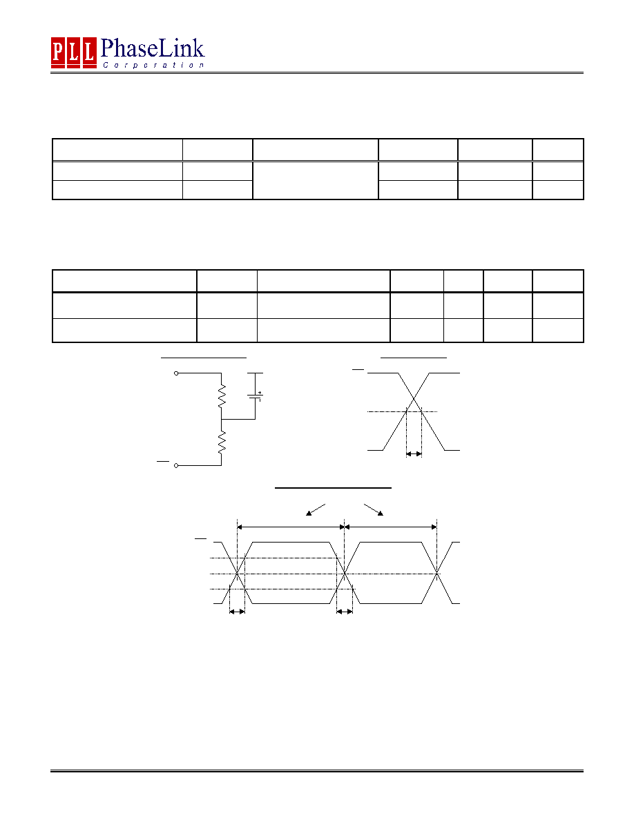
1.0
ns
OUT
OUT
V
OD
V
OS
50
50
OUT
V
DIFF
R
L
= 100
C
L
= 10pF
C
L
= 10pF
LVDS Switching Test Circuit
LVDS Levels Test Circuit
LVDS Transistion Time Waveform
OUT
OUT
OUT
0V (Differential)
0V
20%
80%
20%
80%
t
R
t
F
V
DIFF
PLL620-88/-89
Low Phase Noise XO (9.5-65MHz Output)
47745 Fremont Blvd., Fremont, California 94538 Tel (510) 492-0990 Fax (510) 492-0991
www.phaselink.com Rev 12/08/04 Page 5
8. PECL Electrical Characteristics
PARAMETERS
SYMBOL
CONDITIONS
MIN.
MAX.
UNITS
Output High Voltage
V
OH
V
DD
≠ 1.025
V
Output Low Voltage
V
OL
R
L
= 50
to (V
DD
≠ 2V)
(see figure)
V
DD
≠ 1.620
V
9. PECL Switching Characteristics
PARAMETERS
SYMBOL
CONDITIONS
MIN.
TYP.
MAX.
UNITS
Clock Rise Time
t
r
@20/80% - PECL
0.6
1.5
ns
Clock Fall Time
t
f
@80/20% - PECL
0.5
1.5
ns
OUT
OUT
50
50
PECL Levels Test Circuit
PECL Transistion Time Waveform
OUT
OUT
50%
20%
80%
t
R
t
F
VDD
DUTY CYCLE
45 - 55%
55 - 45%
50%
OUT
OUT
t
SKEW
PECL Output Skew
2.0V

PLL620-88/-89
Low Phase Noise XO (9.5-65MHz Output)
47745 Fremont Blvd., Fremont, California 94538 Tel (510) 492-0990 Fax (510) 492-0991
www.phaselink.com Rev 12/08/04 Page 6
PACKAGE INFORMATION
C
L
A
E
H
D
A1
e
B
16 PIN TSSOP ( mm )
Symbol
Min.
Max.
A
-
1.20
A1
0.05
0.15
B
0.19
0.30
C
0.09
0.20
D
4.90
5.10
E
4.30
4.50
H
6.40 BSC
L
0.45
0.75
e
0.65 BSC
ORDERING INFORMATION
PhaseLink Corporation, reserves the right to make changes in its products or specifications, or both at any time without notice. The information
furnished by Phaselink is believed to be accurate and reliable. However, PhaseLink makes no guarantee or warranty concerning the accuracy of said
information and shall not be responsible for any loss or damage of whatever nature resulting from the use of, or reliance upon this product.
LIFE SUPPORT POLICY: PhaseLink's products are not authorized for use as critical components in life support devices or systems
without the express written approval of the President of PhaseLink Corporation.
For part ordering, please contact our Sales Department:
47745 Fremont Blvd., Fremont, CA 94538, USA
Tel: (510) 492-0990 Fax: (510) 492-0991
PART NUMBER
The order number for this device is a combination of the following:
Device number, Package type and Operating temperature range
PLL620-8x x C
Order Number
Marking
Package Option
PLL620-88OC-R
P620-88 OC
TSSOP ≠ Tape and Reel
PLL620-88OC
P620-88 OC
TSSOP ≠ Tube
PLL620-89OC-R
P620-89 OC
TSSOP ≠ Tape and Reel
PLL620-89OC
P620-89 OC
TSSOP ≠ Tube
PART NUMBER
TEMPERATURE
C=COMMERCIAL
I=INDUSTRIAL
PACKAGE TYPE
O=TSSOP