 | –≠–ª–µ–∫—Ç—Ä–æ–Ω–Ω—ã–π –∫–æ–º–ø–æ–Ω–µ–Ω—Ç: P650-06SC | –°–∫–∞—á–∞—Ç—å:  PDF PDF  ZIP ZIP |
PLL650-06
Network LAN Clock
47745 Fremont Blvd., Fremont, California 94538 Tel (510) 492-0990 Fax (510) 492-0991 www.phaselink.com Rev 09/03/04 Page 1
FEATURES
∑ Full CMOS output swing with 40-mA output drive
capability. 25-mA output drive at TTL level.
∑ Advanced, low power, sub-micron CMOS processes.
∑ 25MHz fundamental crystal or clock input.
∑ One output fixed at 50MHz
∑ One selectable frequency output of 66.6 or 75MHz (with
Double Drive Strength output).
∑ Zero PPM synthesis error in all clocks.
∑ Ideal for Network switches.
∑ 3.3V operation.
∑
Available in 8-Pin 150mil SOIC
.
DESCRIPTION
The PLL 650-06 is a low cost, low jitter, and high
performance clock synthesizer. Using PhaseLink's
proprietary analog Phase Locked Loop techniques, this
device can produce one 50MHz output clock and one
selectable 75MHz or 66.6MHz output clock from a single
low cost 25.0MHz crystal. This makes the PLL650-06 ideal
for networking applications.
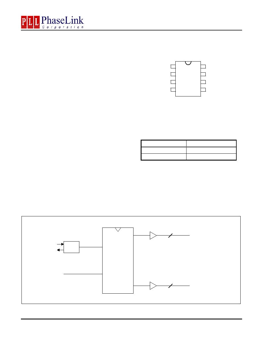
PIN CONFIGURATION
*: bi-directional pin
+ : double strength output
FREQUENCY TABLE
FS Pin
6
0 75MHz
1 66.6MHz
BLOCK DIAGRAM
XTAL
OSC
50MHz
XIN
XOUT
75MHz/66MHz
Control
Logic
FS
1
PLL650-06
1
2
3
4
5
6
7
8
XIN
XOUT
GND
50MHz/FS*
VDD
75MHz
+
/66MHz
+
VDD
GND
PLL650-06
Network LAN Clock
47745 Fremont Blvd., Fremont, California 94538 Tel (510) 492-0990 Fax (510) 492-0991 www.phaselink.com Rev 09/03/04 Page 2
PIN DESCRIPTIONS
Name Number
Type
Description
XIN
1
I
25MHz fundamental crystal input (20pF C
L
parallel resonant).
XOUT 2
I
Crystal
connection
pin.
50MHz/FS 4
B
50MHz outputs. This pin latches the FS input value at power-up. It has a
60k
internal pull up resistor.
75MHz / 66MHz
6
O
75MHz or 66.6MHz outputs with double drive strength. The output frequency
is determined by the value of FS (see pin 4).
VDD
5, 8
P
3.3V power supply.
GND 3,
7
P
Ground.
FUNCTIONAL DESCRIPTION
Selectable spread spectrum and output frequencies
The PLL650-06 provides selectable output frequencies. Selection is made by connecting the selector pin to a logical "zero" or
"one", or by leaving it not connected (internal pull-up) according to the frequency selection table shown on page 1.
Pin 4 (FS) is a bi-directional pin used to select the output frequency of pin 6 (75MHz or 66.6MHz) according to the Frequency
Selection Table on page 1. The description of how to connect this bi-directional pin follows in the next paragraph.
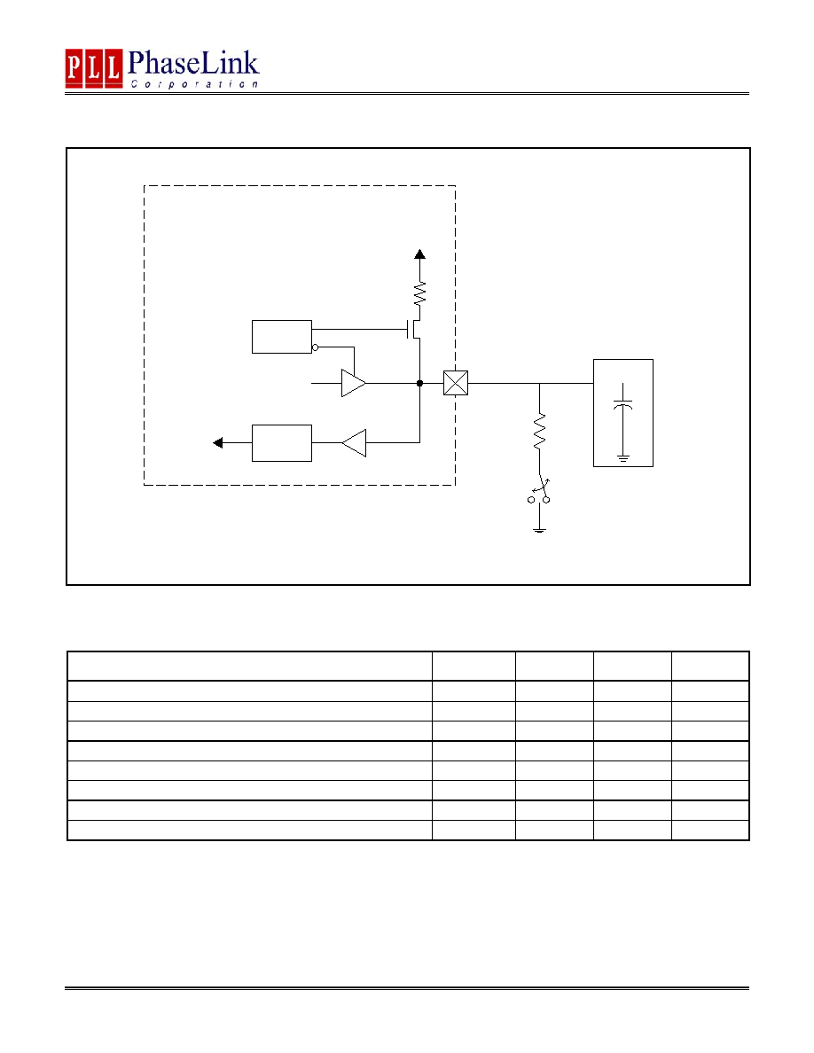
Connecting a bi-directional pin
A bi-directional pin serves as input upon power-up, and as output as soon as the inputs have been latched. The value of the
input is latched-in upon power-up. Depending on the pin (see pin description), the input can be tri-level or a standard two-level.
Unlike unidirectional pins, bi-directional pins cannot be connected directly to GND or VDD in order to set the input to "0" or "1",
since the pin also needs to serve as output. In the case of two level input pins, an internal pull-up resistor is present. This allows
a default value to be set when no external pull down resistor is connected between the pin and GND (by definition, a tri-level
input has a the default value of "M" (mid) if it is not connected). In order to connect a bi-directional pin to a non-default value, the
input must be connected to GND or VDD through an external pull-down/pull-up resistor. Note: when the output load presents a
low impedance in comparison to the internal pull-up resistor, the internal pull-up resistor may not be sufficient to pull the input up
to a logical "one", and an external pull-up resistor may be required.
For bi-directional inputs, the external loading resistor between the pin and GND has to be sufficiently small (compared to the
internal pull-up resistor) so that the pin voltage be pulled below 0.8V (logical "zero"). In order to avoid loading effects when the
pin serves as output, the value of the external pull-down resistor should however be kept as large as possible. In general, it is
recommended to use an external resistor of around one sixth to one quarter of the internal pull-up resistor (see Application
Diagram). Note: when the output is used to drive a load presenting an small resistance between the output pin and VDD, this
resistance is in essence connected in parallel to the internal pull-up resistor. In such a case, the external pull-down resistor may
have to be dimensioned smaller to guarantee that the pin voltage will be low enough achieve the desired logical "zero". This is
particularly true when driving 74FXX TTL components.
PLL650-06
Network LAN Clock
47745 Fremont Blvd., Fremont, California 94538 Tel (510) 492-0990 Fax (510) 492-0991 www.phaselink.com Rev 09/03/04 Page 3
APPLICATION DIAGRAM
Electrical Specifications
1. Absolute Maximum Ratings
PARAMETERS SYMBOL
MIN.
MAX.
UNITS
Supply Voltage
V
DD
4.6 V
Input Voltage, dc
V
I
-0.5
V
DD
+0.5 V
Output Voltage, dc
V
O
-0.5
V
DD
+0.5 V
Storage Temperature
T
S
-65 150
∞C
Ambient Operating Temperature*
T
A
-40 85
∞C
Junction Temperature
T
J
125
∞C
Lead Temperature (soldering, 10s)
260
∞C
ESD Protection, Human Body Model
2
kV
Exposure of the device under conditions beyond the limits specified by Maximum Ratings for extended periods may cause permanent damage to the device
and affect product reliability. These conditions represent a stress rating only, and functional operations of the device at these or any other conditions above
the operational limits noted in this specification is not implied.
* Note: Operating Temperature is guaranteed by design for all parts (COMMERCIAL and INDUSTRIAL), but tested for COMMERCIAL grade only.
Latch
Power Up
Reset
Jumper options
R
UP
/
4
Clock Load
Latched
Input
Output
EN
VDD
R
up
Bi-directional pin
R
RB
NOTE: Rup=60k
. R starts from 1 to 0 while RB starts from 0 to 1.
Internal to chip
External Circuitry
PLL650-06
Network LAN Clock
47745 Fremont Blvd., Fremont, California 94538 Tel (510) 492-0990 Fax (510) 492-0991 www.phaselink.com Rev 09/03/04 Page 4
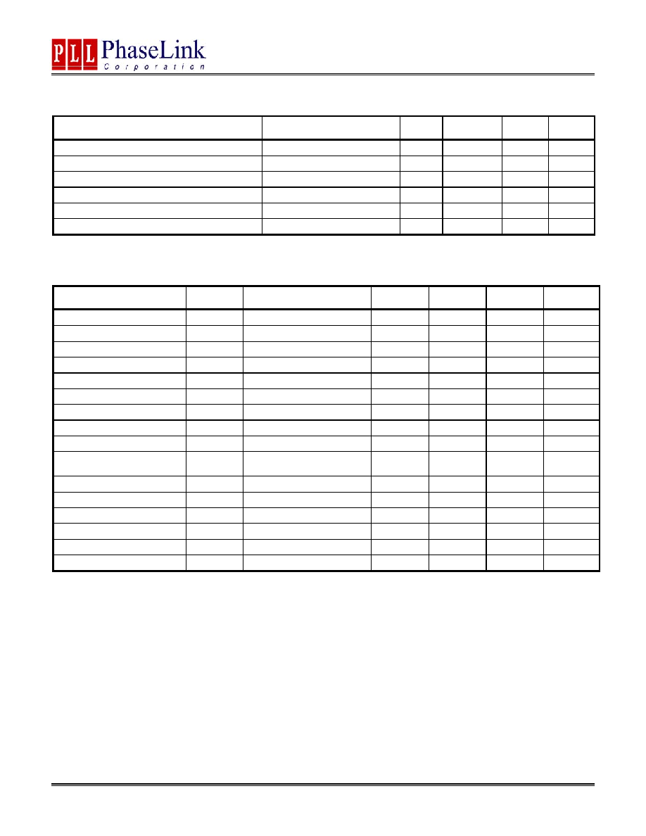
2. AC Specifications
PARAMETERS
CONDITIONS
MIN. TYP. MAX.
UNITS
Input Frequency
10
25
27
MHz
Output Rise Time
0.8V to 2.0V with no load
1.5
ns
Output Fall Time
2.0V to 0.8V with no load
1.5
ns
Duty Cycle
@ 50% V
DD
45
50
55
%
Max. Absolute Jitter
Short term
±150
ps
Max. Jitter, cycle to cycle
80
ps
3. DC Specifications
PARAMETERS SYMBOL CONDITIONS MIN. TYP. MAX.
UNITS
Operating Voltage
V
DD
2.97
3.63
V
Input High Voltage
V
IH
V
DD
/2
V
Input Low Voltage
V
IL
V
DD
/2
V
DD
/2 - 1
V
Input High Voltage
V
IH
For all Tri-level input
V
DD
-0.5
V
Input Low Voltage
V
IL
For all Tri-level input
0.5
V
Input High Voltage
V
IH
For all normal input
2
V
Input Low Voltage
V
IL
For all normal input
0.8
V
Output High Voltage
V
OH
I
OH
= -25mA
2.4
V
Output Low Voltage
V
OL
I
OL
= 25mA
0.4
V
Output High Voltage At
CMOS Level
V
OH
I
OH
= -8mA
V
DD
-0.4
V
Operating Supply Current
I
DD
No Load
35
mA
Short-circuit Current
I
S
±50
mA
Nominal output current*
I
out
CMOS
output
level
35
40
mA
Nominal output current*
I
out
TTL output level
20
25
mA
Internal pull-up resistor
R
up
Pins 5,7
60
k
Internal pull-up resistor
R
up
Pin 2
120
k
*: Output strengths are doubled (i.e. min. CMOS level is 70mA, typ. CMOS level is 80mA) on pin 6 (output for 75MHz or 66.6MHz)
PLL650-06
Network LAN Clock
47745 Fremont Blvd., Fremont, California 94538 Tel (510) 492-0990 Fax (510) 492-0991 www.phaselink.com Rev 09/03/04 Page 5
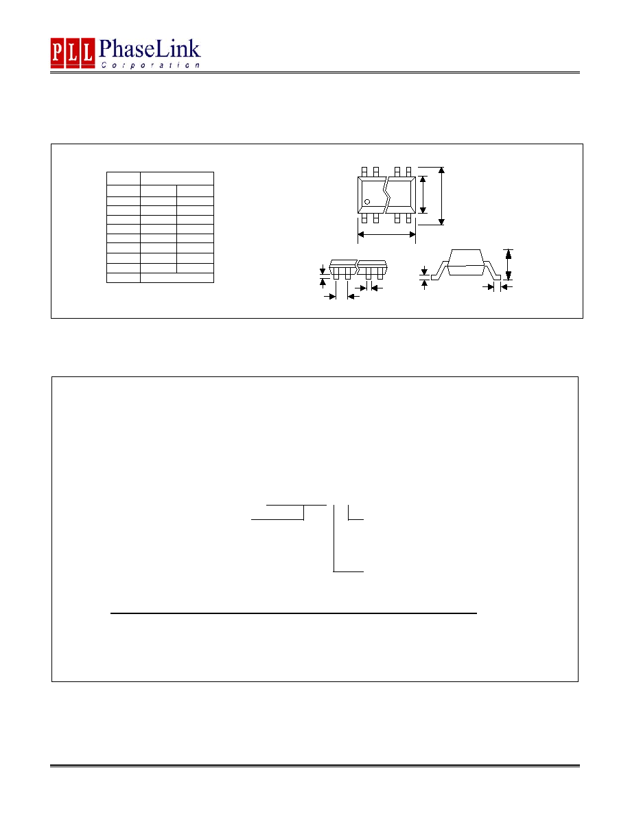
PACKAGE INFORMATION
ORDERING INFORMATION
PhaseLink Corporation, reserves the right to make changes in its products or specifications, or both at any time without notice. The information
furnished by Phaselink is believed to be accurate and reliable. However, PhaseLink makes no guarantee or warranty concerning the accuracy of said
information and shall not be responsible for any loss or damage of whatever nature resulting from the use of, or reliance upon this product.
LIFE SUPPORT POLICY: PhaseLink's products are not authorized for use as critical components in life support devices or systems without the
express written approval of the President of PhaseLink Corporation.
For part ordering, please contact our Sales Department:
47745 Fremont Blvd., Fremont, CA 94538, USA
Tel: (510) 492-0990 Fax: (510) 492-0991
PART NUMBER
The order number for this device is a combination of the following:
Device number, Package type and Operating temperature range
PLL650-06 S C
Order Number
Marking
Package Option
PLL650-06SC-R
P650-06SC
SOIC - Tape and Reel
PLL650-06SC
P650-06SC
SOIC - Tube
PART NUMBER
TEMPERATURE
C=COMMERCIAL
I=INDUSTRAL
PACKAGE TYPE
S=SOIC
C
L
A
8 PIN ( dimensions in mm )
Narrow SOIC
Symbol
Min.
Max.
A
1.47
1.73
A1
0.10
0.25
B
0.33
0.51
C
0.19
0.25
D
4.80
4.95
E
3.80
4.00
H
5.80
6.20
L
0.38
1.27
e
1.27 BSC
E
H
D
A
1
e
B