 | –≠–ª–µ–∫—Ç—Ä–æ–Ω–Ω—ã–π –∫–æ–º–ø–æ–Ω–µ–Ω—Ç: P701-10DC | –°–∫–∞—á–∞—Ç—å:  PDF PDF  ZIP ZIP |

PLL701-10
Low EMI Spread Spectrum Multiplier IC (in Die or Package)
47745 Fremont Blvd., Fremont, California 94538 Tel (510) 492-0990 Fax (510) 492-0991 www.phaselink.com Rev 09/20/04 Page 1
FEATURES
∑ Spread Spectrum Clock Generator/Multiplier with
output selectable from 1x to 8x.
∑ 13MHz to 240MHz output with output enable.
∑ 13MHz to 30 MHz reference input frequency
accepted from crystal or external clock signal.
∑ Reduced EMI from Spread Spectrum Modulation,
with selectable modulation amplitude for Center
Spread, Down Spread or Asymmetric Spread.
∑ TTL/CMOS compatible outputs.
∑ 3.3V Operating Voltage.
∑ 150 ps maximum cycle-to-cycle jitter.
∑ Available in 16-Pin 150mil SSOP or DIE.
DESCRIPTION
The PLL701-10 is a low EMI Clock Generator and
Multiplier for high-speed digital systems. It uses
Spread Spectrum Technology (SST) and permits
different levels of EMI reduction by selecting the
amplitude of the applied SST. The SST feature can
be turned off. An output enable input is also used.
The chip operates with input frequencies ranging from
13 to 30 MHz and provides 1x to 8x at its output.
OUTPUT CLOCK (FOUT) SELECTION
M2 M1 M0 FIN/XIN
(MHz)
Multiplier
FOUT
(MHz)
0
0
0
13 ~ 28
X1
13 ~ 28
0
0
1
13 ~ 28
X2
26 ~ 56
0
1
0
14 ~ 30
X3
42 ~ 90
0
1
1
13 ~ 28
X4
52 ~ 112
1
0
0
20 ~ 30
X5
100 ~ 150
1
0
1
17 ~ 30
X6
102 ~ 180
1
1
0
15 ~ 30
X7
105 ~ 210
1
1
1
13 ~ 28
X8
104 ~ 224
BLOCK DIAGRAM
PACKAGE PIN CONFIGURATION
DIE PAD CONFIGURATION
Note: ^: Internal pull-up resistor (120k
for SD0, 30 k for SC0-
SC2, SD1, M0-M2 and OE). The internal pull-up resistor
results in a default high value when no pull-down resistor is
connected to this pin.
*: SD0 and SD1 are latched upon power-up.
PLL 701-10
1
2
3
4
5
6
7
8
XIN/FIN
9
10
11
12
13
14
15
16
XOUT/SD0*^
M2^
M1^
M0^
SC0^
SC1^
SC2^
GND
AVDD
REF/SD1*^
VDD
SC3^
OE^
FOUT
GND
XIN/FIN = 10 ~ 30 MHz
XTAL
OSC
FOUT
XIN
XOUT
M(0:2)
SD(0:1)
SC(0:3)
PLL
SST
Control
Logic
OE
XOUT/SD0*^
GNDOSC
M2^
M1^
SC0^
M0^
SC1^
AVDD
AVDD
REF/SD1*^
VDD
VDD (optional)
VDD (optional)
SC3^
OE^
FOUT
GNDBUF
GND
GND
GND
SC
2^
XI
N
GN
D
GN
D
AV
DD
(
O
pt
io
nal)
(
O
pt
io
nal)
1
10
8
7
6
5
4
17
16
15
14
13
12
18
35
34
30
29
28
25
23
22
21
20
19
Y
X
104
mil
69 mil
1700, 2540
C501A
A0404
-04A
PLL701-10
Low EMI Spread Spectrum Multiplier IC (in Die or Package)
47745 Fremont Blvd., Fremont, California 94538 Tel (510) 492-0990 Fax (510) 492-0991 www.phaselink.com Rev 09/20/04 Page 2
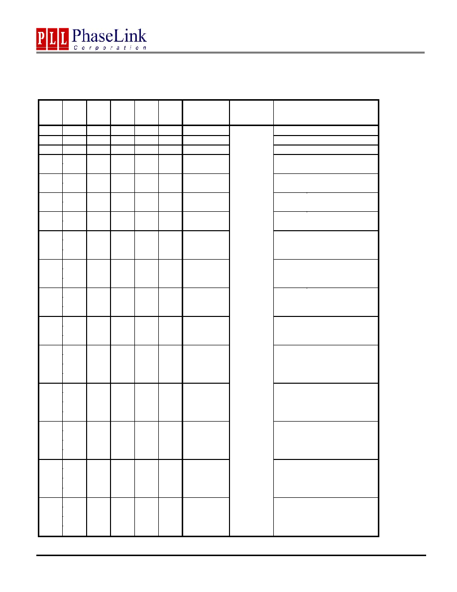
SPREAD SPECTRUM SELECTION TABLE
Notes: C: Center Spread. A: Asymmetric Spread. D: Down Spread.
SD1 SD0 SC3 SC2 SC1 SC0
Modulation
Magnitude
Modulation
Frequency
Modulation Type
1 1 0 0 0 0 0.250%
C ±
0.125%
1 1 0 0 0 1 0.500%
C ±
0.25%
1 1 0 0 1 0 0.750%
C ±
0.375%
1 1 0 0 1 1
C
±
0.50%
1 0 0 0 1 1
1.000%
D -1.00%
1 1 0 1 0 0
C
±
0.625%
1 0 0 1 0 0
1.250%
A +0.125
~
-1.125%
1 1 0 1 0 1
C
±
0.75%
1 0 0 1 0 1
1.500%
A +0.25
~
-1.25%
1 1 0 1 1 0
C
±
0.875%
1 0 0 1 1 0
1.750%
A +0.375
~
-1.375%
1 1 0 1 1 1
C
±
1.00%
1 0 0 1 1 1
A
+0.50
~
-1.5%
0 1 0 1 1 1
2.000%
D -2.00%
1 1 1 0 0 0
C
±
1.125%
1 0 1 0 0 0
A
+0.625
~
-1.625%
0 1 1 0 0 0
2.250%
A +0.125
~
-2.125%
1 1 1 0 0 1
C
±
1.25%
0 1 1 0 0 1
A
+0.25
~
-2.25%
1 0 1 0 0 1
2.500%
A +0.75
~
-1.75%
1 1 1 0 1 0
C
±
1.375%
1 0 1 0 1 0
A
+0.875
~
-1.875%
0 1 1 0 1 0
2.750%
A +0.375
~
-2.375%
1 1 1 0 1 1
C
±
1.50%
0 0 1 0 1 1
D
-3.00%
1 0 1 0 1 1
A
+1.00
~
-2.00%
0 1 1 0 1 1
3.000%
A +0.50
~
-2.50%
1 1 1 1 0 0
C
±
1.625%
1 0 1 1 0 0
A
+1.125
~
-2.125%
0 1 1 1 0 0
A
+0.625
~
-2.625%
0 0 1 1 0 0
3.250%
A +0.125
~
-3.125%
1 1 1 1 0 1
C
±
1.75%
1 0 1 1 0 1
A
+1.25
~
-2.25%
0 1 1 1 0 1
A
+0.75
~
-2.75%
0 0 1 1 0 1
3.500%
A +0.25
~
-3.25%
1 1 1 1 1 0
C
±
1.875%
1 0 1 1 1 0
A
+1.37
~
-2.375%
0 1 1 1 1 0
A
+0.875
~
-2.875%
0 0 1 1 1 0
3.750%
A +0.375
~
-3.375%
1 1 1 1 1 1
SST
turned
off
1 0 1 1 1 1
SST
turned
off
0 1 1 1 1 1
SST
turned
off
0 0 1 1 1 1
0.00 %
Fin / 512
SST
turned
off

PLL701-10
Low EMI Spread Spectrum Multiplier IC (in Die or Package)
47745 Fremont Blvd., Fremont, California 94538 Tel (510) 492-0990 Fax (510) 492-0991 www.phaselink.com Rev 09/20/04 Page 3
PIN/PAD DESCRIPTIONS
Name
Pin #
Pad #
Type
Description
XIN/FIN 1 22 I
Crystal input to be connected to fundamental parallel mode crystal.
(C
L
=20pF) or clock input.
XOUT/SD0 2
23 B
At power-up, this pin is acts as input pin to select the modulation
rate and is latched in. After the input sampling, it is used as crystal
output connector. 120k
internal pull up resistor.
M2 3 28
I
Digital control input to select output frequency. 30k
internal pull-
up.
M1 4 29
I
Digital control input to select output frequency. 30k
internal pull-
up.
M0 5 30
I
Digital control input to select output frequency. 30k
internal pull-
up.
SC0 6 34 I
Digital control input to select spread spectrum modulation.
30k
internal pull-up.
SC1 7 35 I
Digital control input to select spread spectrum modulation.
30k
internal pull-up.
SC2 8 1 I
Digital control input to select spread spectrum modulation.
30k
internal pull-up.
SC3 12 12 I
Digital control input to select spread spectrum modulation.
30k
internal pull-up.
FOUT 10 8 O
Modulated Clock Frequency Output. The frequency before
modulation is synthesized by multiplying the input frequency by 1X
to 8X, depending on SD(0:1) and SC(0:3).
OE 11 10 I
Output Enable. When low, Tri-states all outputs.
30k
internal pull-up.
VDD 13
13,14,15
P
3.3V
Power
Supply.
REF/SD1 14
16 B
At power-up, this pin acts as input pin to select the modulation rate
and is latched in. After the input sampling, this pin provides a
buffered Reference Clock Output of the same frequency as the
crystal or clock input. 30k
internal pull-up.
AVDD
15
17,18,19
P
3.3V Analog power supply.
GNDOSC
N/A
25
P
Ground for Oscillator circuitry.
GNDBUF
N/A
7
P
Ground for output buffer circuitry.
GND
9 and 16
4,5,6,20,21
P
Ground.
Notes: B ≠ bi-directional pin; I ≠ input pin; P ≠ power supply/ground pin.
DIE SPECIFICATIONS
Name Value
Size
104 x 69 mil
Reverse side
GND
Pad dimensions
80 micron x 80 micron
Thickness 10
mil
PLL701-10
Low EMI Spread Spectrum Multiplier IC (in Die or Package)
47745 Fremont Blvd., Fremont, California 94538 Tel (510) 492-0990 Fax (510) 492-0991 www.phaselink.com Rev 09/20/04 Page 4
FUNCTIONAL DESCRIPTION
Selectable spread spectrum and modulation rates
The PLL701-10 provides selectable multiplier factors (1x to 8X), selectable spread spectrum modulation, as well as
selectable modulation rate. Selection is made by connecting specific input pins to a logical "zero" or "one". Pins 6
(SC0), 7 (SC1), 8 (SC2) and 12 (SC3) are used as inputs to select the spread spectrum modulation as shown on
the spread spectrum selection table (page 2). Pins 3 (M2), 4 (M1), 5 (M0) are used as inputs to select the output
frequency as shown on the output clock selection table (page 1). Pin 11 is the output enable pin, that tri-states all
outputs when low (logical "zero").
In order to reduce the number of pins on the chip, the PLL701-10 uses pin 2 and 14 (XOUT/SD0 and REF/SD1) as
a bi-directional pin. The pins serve as modulation rate selector inputs (SD0 and SD1) upon power-up (see
modulation rate table on page 1), and as XOUT crystal connection (pin 2), and REF output signal (pin 14) as soon
as the inputs have been latched.
Connecting a selection pin to a logical "one"
All selection pins have an internal pull-up resistor (30k
for pins 3, 4, 5, 6, 7, 8, 11, 12, 14 and 120k for pin 2).
This internal pull-up resistor will pull the input value to a logical "one" (pull-up) by default, i.e. when no resistive
load is connected between the pin and GND. No external pull-up resistor is therefore required for connecting a
logical "one" upon power-up.
Connecting a selection pin to a logical "zero"
For an input only pin, i.e. all input pins except XOUT/SD0 (pin 2) and REF/SD1 (pin 14), the pin simply needs to be
grounded to pull the input down to a logical "zero". Connecting the bi-directional pins (SD0 and SD1) to a logical
"zero" will however require the use of an external loading resistor between the pin and GND that has to be
sufficiently small (compared to the internal pull-up resistor) so that the pin voltage be pulled below 0.8V (logical
"zero"). In order to avoid loading effects when the pin serves as output, the value of the external pull-down resistor
should however be kept as large as possible. In general, it is recommended to use an external resistor of around
Rup/4 (e.g. 27k
for pin 2 and 4.7k for pin 14, see Application Diagram).
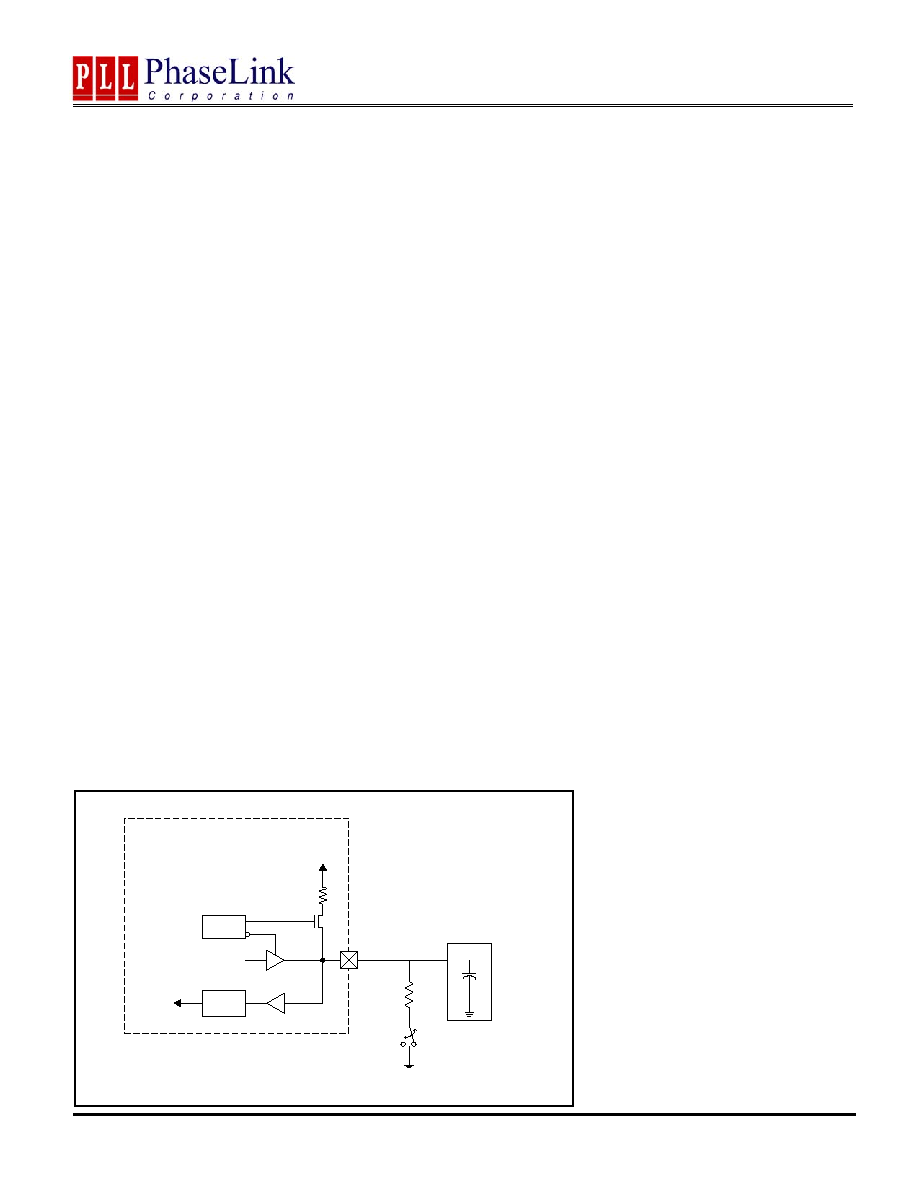
APPLICATION DIAGRAM FOR OUTPUT AND MODULATION SELECTION
Latch
Power Up
Reset
Jumper
options
R
up
/4
Clock Load
SD0 or
SC0~SC2
XIN
EN
VDD
R
up
Bi-directional pin
R
RB
NOTE: Rup=120k
for SD0 (Pin2); and Rup=30k for SD1(Pin 14). R starts from 1 to 0 while RB starts from 0 to 1.
Internal to chip
External Circuitry

PLL701-10
Low EMI Spread Spectrum Multiplier IC (in Die or Package)
47745 Fremont Blvd., Fremont, California 94538 Tel (510) 492-0990 Fax (510) 492-0991 www.phaselink.com Rev 09/20/04 Page 5
ELECTRICAL SPECIFICATIONS
1. Absolute Maximum Ratings
PARAMETERS SYMBOL
MIN.
MAX.
UNITS
Supply Voltage
V
DD
4.6 V
Input Voltage, dc
V
I
-0.5
V
DD
+0.5 V
Output Voltage, dc
V
O
-0.5
V
DD
+0.5 V
Storage Temperature
T
S
-65 150
∞C
Ambient Operating Temperature*
T
A
-40 85
∞C
Junction Temperature
T
J
125
∞C
Lead Temperature (soldering, 10s)
260
∞C
ESD Protection, Human Body Model
2
kV
Exposure of the device under conditions beyond the limits specified by Maximum Ratings for extended periods may cause permanent damage to the
device and affect product reliability. These conditions represent a stress rating only, and functional operations of the device at these or any other
conditions above the operational limits noted in this specification is not implied.
* Note: Operating Temperature is guaranteed by design for all parts (COMMERCIAL and INDUSTRIAL), but tested for COMMERCIAL grade only.
2. DC/AC Specifications
PARAMETERS SYMBOL CONDITIONS MIN.
TYP.
MAX.
UNITS
Supply Voltage
V
DD
2.97 3.63 V
Input High Voltage
V
IH
0.7*
V
DD
V
Input Low Voltage
V
IL
0.3*
V
DD
V
Input High Current
I
IH
100
µA
Input Low Current
I
IL
100
µA
Output High Voltage
V
OH
I
OH
=5mA, V
DD
=3.3V
2.4
Output Low Voltage
V
OL
I
OL
=6mA, V
DD
=3.3V 0.4
F
XIN
When using a crystal
15
30
MHz
Input Frequency
F
IN
When using reference clock
15
30
MHz
Maximum interruption of F
IN
When using reference clock
100
µs
Load Capacitance
C
L
Between Pin XIN and
XOUT*
18 pF
Pull-up Resistor
R
up
PIN
2
120 k
Pull-up Resistor
R
up
PIN
3,4,5,6,7,8,11,12 30 k
Short Circuit Current
I
sc
25 mA
3.3V Dynamic Supply Current
I
CC
No
Load
20 mA
*Note: Pin XIN and XOUT each has a 36pF capacitance. When used with a XTAL, the two capacitors combined load the crystal with 18pF. If driving XIN
with a reference clock signal, the load capacitance will be 36pF (typical).