
(Preliminary)
PL580-30
38MHz-640MHz Low Phase Noise VCXO
47745 Fremont Blvd., Fremont, California 94538 Tel (510) 492-0990 Fax (510) 492-0991 www.phaselink.com Rev 11/30/05 Page 1
FEATURES
∑ Less than 0.4ps RMS (12KHz-20MHz) phase
jitter for
all frequencies
.
∑ Low phase noise output (@ 1MHz frequency
offset
-140dBc/Hz for 311.04MHz,
-131dBC/Hz for 622.08MHz
∑ 19MHz-40MHz crystal input.
∑ 38MHz-640MHz output.
∑ Selectable PECL, LVDS, or CMOS outputs.
∑ No external varicap required.
∑ Output Enable selector.
∑ Wide pull range (+/-200ppm).
∑ 3.3V operation.
∑ Available in 3x3 QFN or 16-pin TSSOP
packages.
DESCRIPTION
The PL580-30 is a monolithic low jitter and low
phase noise VCXO, capable of 0.4ps RMS phase
jitter and PECL, LVDS, or CMOS outputs, covering a
wide frequency output range up to 640MHz. It allows
the control of the output frequency with an input
voltage (VCON), using a low cost crystal.
The PL580-30 is designed to address the demanding
requirements of high performance applications such
as SONET, GPS, XDSL, etc.
BLOCK DIAGRAM
DIE CONFIGURATION
Note1: ^ Denotes internal pull up resistor.
DIE SPECIFICATIONS
Name Value
Size
62 x 65 mil
Reverse side
GND
Pad dimensions
80 micron x 80 micron
Thickness 10
mil
18
19
20
21
23
25
7
13
10
26
29
31
Y
X
(0,0)
(1550,1475)
62
m
i
l
65 mil
24
22
17
16
15
14
12
11
9
8
6
1
2
3
4
5
27
28
30
GN
DO
S
C
GN
D
B
UF
GND
D
IG
DNC
LM
LP
GNDA
N
A
DN
C
OE_SEL^
GNDBUF
CMOS
LVDSB
PECLB
VDDBUF
VDDBUF
PECL
LVDS
O
U
T
S
EL1^
SE
L0
^
SE
L1
^
V
DDDI
G
V
DDOSC
V
DDA
N
A
V
DDA
N
A
OUTSEL
0
v
XIN
XOUT
DNC
SEL2
OE_CTRL
VCON
Die ID:
2222-22A
C502A
Phase
Detector
Charge
Pump
Loop
Filter
VCO
(F
XiN
x16)
VCO
Divider
XTAL
OSC
QBAR
OE
XIN
XOUT
Q
VCON
VARICAP
+
Performance Tuner
Output
Divider
(1,2,4,8)
(Preliminary)
PL580-30
38MHz-640MHz Low Phase Noise VCXO
47745 Fremont Blvd., Fremont, California 94538 Tel (510) 492-0990 Fax (510) 492-0991 www.phaselink.com Rev 11/30/05 Page 2
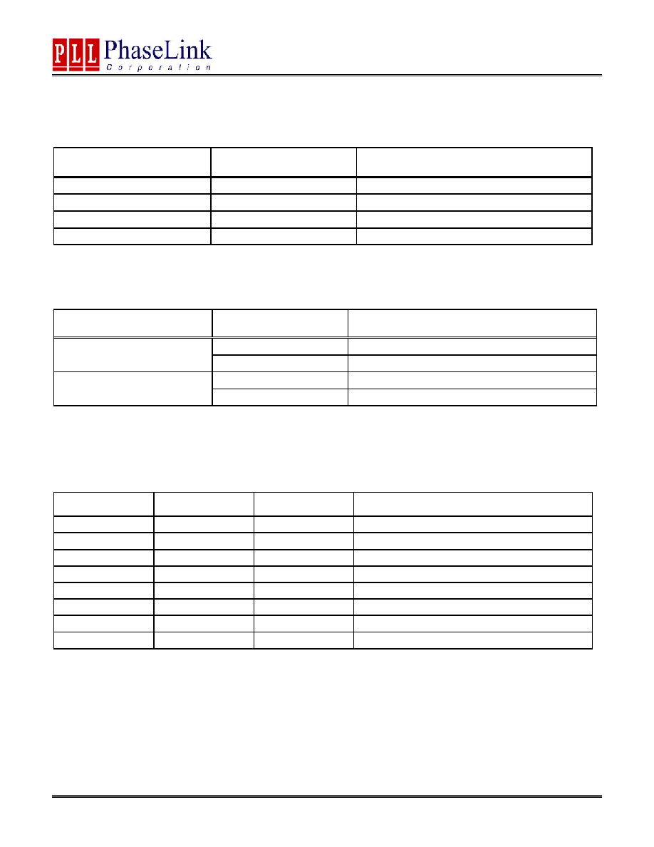
OUTPUT ENABLE LOGICAL LEVELS
OUTSEL0
v
(Pad #25)
OUTSEL1^
(Pad #18)
Selected Output
0 0
LVDS
0 1 PECL
(Default)
1
0
High Drive CMOS
1
1
Standard Drive CMOS
Note: For bonding convenience, `OUTSEL0' incorporates an internal pull down resistor while `OUTSEL1' incorporates an internal pull up resistor.
OUTPUT SELECTION AND ENABLE
OE_SEL^
(Pad #9)
OE_CTRL
(Pad #30)
State
0 (Default)
Output enabled
0
1 Tri-state
0 Tri-state
1 (Default)
1 (Default)
Output enabled
Pad #9: Bond to GND to set to "0", bond to VDD to set to "1",
Pad #30: Logical states defined by PECL levels if OE_SELECT is "0"
Logical states defined by CMOS levels if OE_SELECT is "1"
FREQUENCY SELECTION TABLE
SEL2 SEL1
SEL0
Selected Multiplier/Output Frequency
0 0 0
VCO
Max*
0 0 1
VCO
Min*
0 1 0
Reserved
0 1 1
Reserved
1 0 0
Fin
x
2
1 0 1
Fin
x
8
1 1 0
Fin
x
16
1 1 1
Fin
x
4
All SEL pads have internal pull-ups (default value is `1'). Bond to GND to set to 0.
* Special Test Modes to help selecting the inductor value for the target output frequency.

(Preliminary)
PL580-30
38MHz-640MHz Low Phase Noise VCXO
47745 Fremont Blvd., Fremont, California 94538 Tel (510) 492-0990 Fax (510) 492-0991 www.phaselink.com Rev 11/30/05 Page 3
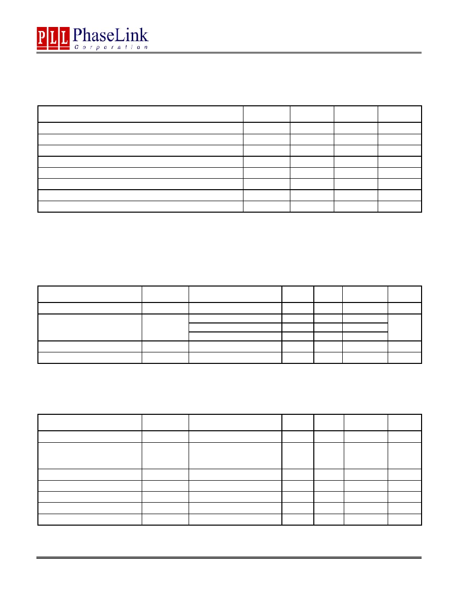
PAD ASSIGNMENT
Pad #
Name
X (
µm) Y
(
µm)
Description
1 GNDOSC 248 109
Ground, Oscillator circuitry.
2
GNDANA
361
109
Ground, Analog circuitry.
3 LP 473
109
Performance/Frequency
tuning
Inductor.
4 LM 587
109
Performance/Frequency tuning Inductor.
5
DNC
702
109
Do No Connect.
6
DNC
874
109
Do No Connect.
7 GNDDIG 1042
109
Ground, Digital circuitry.
8
GNDBUF
1171
109
Ground, buffer circuitry.
9 OE_SELECT 1400 125
Used to select between PECL or CMOS logic states for OE.
Incorporates internal pull up.
10 LVDS 1400
259
LVDS Output.
11 PECL 1400
476
PECL
Output.
12
VDDBUF
1400
616
3.3V power supply, Buffer circuitry.
13
VDDBUF
1400
716
3.3V power supply, Buffer circuitry.
14 PECLB 1400
871
Complementary PECL Output.
15
LVDSB
1400
1089
Complementary LVDS Output.
16
CMOS
1400
1227
Single ended CMOS output.
17 GNDBUF 1389
1365
Ground, buffer circuitry.
18 OUTSEL1 1232 1365
Used to select CMOS, PECL or LVDS output type. Incorporates
internal pull up.
19 SEL1 1042
1365
20 SEL0 854
1365
Used to select multiplication factor. Incorporates internal pull up.
21 VDDDIG 659
1365
3.3V
power
supply, Digital circuitry.
22
VDDANA
559
1365
3.3V power supply, Analog circuitry.
23
VDDANA
459
1365
3.3V power supply, Analog circuitry.
24 VDDOSC 358 1365
3.3V power supply, Oscillator circuitry.
25 OUTSEL0B 194 1365
Used to select CMOS, PECL or LVDS output type. Incorporates
internal pull down.
26
XIN
109
1223
Crystal input. See crystal specification for details.
27 XOUT 109
1017
Crystal output. See crystal specification for details.
28
SEL2
109
858
Used to select multiplication factor. Incorporates internal pull up.
29
DNC
109
646
Do Not Connect
30 OE_CTRL 109 397
Used to enable/disable the output(s). See Output Selection and
Enable table.
31 VCON 109
181
Voltage Control Input. 0V to 3.3V.

(Preliminary)
PL580-30
38MHz-640MHz Low Phase Noise VCXO
47745 Fremont Blvd., Fremont, California 94538 Tel (510) 492-0990 Fax (510) 492-0991 www.phaselink.com Rev 11/30/05 Page 4
PERFORMANCE TUNING & INDUCTOR VALUE SELECTION
Please refer to PhaseLink's `PhasorV Tuning Assistance' software to automatically calculate the optimum inductor
values for your application. In addition, the chart below could be used as a reference for quick inductor value
selection. Please note that the inductor values mentioned in the table below, or when using `PhasorV Tuning
Assistance' are derived based on the parasitic values of PhaseLink's evaluation board. For performance
enhancement of your custom board design, please follow the following instruction:
Use the special test modes "VCO Max" and "VCO Min" to determine the optimum inductor value. "VCO Max"
represents the high end of the VCO range and "VCO Min" represents the low end of the VCO range. The output
frequency in the "VCO Max" and "VCO Min" test modes is VCO/16. This means that the output frequencies are
around the crystal frequency that will be used. The optimum inductor value is where the target crystal frequency
is closest to the middle between the "VCO Max" and "VCO Min" output frequencies. In this case the VCO will lock
in the middle of its tuning range with maximum margin on either side.
(Preliminary)
PL580-30
38MHz-640MHz Low Phase Noise VCXO
47745 Fremont Blvd., Fremont, California 94538 Tel (510) 492-0990 Fax (510) 492-0991 www.phaselink.com Rev 11/30/05 Page 5
ELECTRICAL SPECIFICATIONS
1. Absolute Maximum Ratings
PARAMETERS SYMBOL
MIN.
MAX.
UNITS
Supply Voltage
V
DD
4.6 V
Input Voltage, dc
V
I
-0.5
V
DD
+0.5 V
Output Voltage, dc
V
O
-0.5
V
DD
+0.5 V
Storage Temperature
T
S
-65 150
∞C
Ambient Operating Temperature*
T
A
-40 85
∞C
Junction Temperature
T
J
125
∞C
Lead Temperature (soldering, 10s)
260
∞C
ESD Protection, Human Body Model
2
kV
Exposure of the device under conditions beyond the limits specified by Maximum Ratings for extended periods may cause permanent damage to the
device and affect product reliability. These conditions represent a stress rating only, and functional operations of the device at these or any other
conditions above the operational limits noted in this specification is not implied.
* Note: Operating Temperature is guaranteed by design for all parts (COMMERCIAL and INDUSTRIAL), but tested for COMMERCIAL grade only.
2. Crystal Specifications
PARAMETERS SYMBOL CONDITIONS MIN.
TYP.
MAX.
UNITS
Crystal Resonator Frequency
F
XIN
Parallel Fundamental Mode
19
40
MHz
at VCON = 0V
17.7
at VCON = 1.65V
9.5
Crystal Loading Rating
C
L (xtal)
at VCON = 3.3V
5.4
pF
Crystal Pullability
C
0
/C
1 (xtal)
AT
cut
250
-
Recommended ESR
R
E
AT cut
30
Note: Crystal Loading rating: The listed numbers are for the IC only. Specify the crystal for the value at VCON = 1.65V and add the PCB & package
parasitic. A round number (i.e. 12pF) can be achieved by adding external capacitors. Try to add the same value to XIN and XOUT, and please note,
that frequency pulling and oscillator gain may decrease.
3. Voltage Control Crystal Oscillator
PARAMETERS SYMBOL CONDITIONS MIN.
TYP.
MAX.
UNITS
VCXO Stabilization Time *
T
VCXOSTB
From power valid
10
ms
VCXO Tuning Range
F
XIN
= 19 ≠ 40MHz;
XTAL C
0
/C
1
< 250
0V
VCON 3.3V
500 ppm
CLK output pullability
VCON=1.65V,
±1.65V
±200
ppm
VCXO Tuning Characteristic
150
ppm/V
Pull range linearity
10
%
VCON pin input impedance
60
k
VCON modulation BW
0V
VCON 3.3V, -3dB
25
kHz
Note: Parameters denoted with an asterisk (*) represent nominal characterization data and are not production tested to any specific limits.

(Preliminary)
PL580-30
38MHz-640MHz Low Phase Noise VCXO
47745 Fremont Blvd., Fremont, California 94538 Tel (510) 492-0990 Fax (510) 492-0991 www.phaselink.com Rev 11/30/05 Page 6
4. General Electrical Specifications
PARAMETERS SYMBOL
CONDITIONS
MIN. TYP. MAX. UNITS
38MHz<Fout<100MHz
65/45/30
PECL/LVDS/CMOS
100MHz<Fout<320MHz
80/60/40
Supply Current,
Dynamic (with
Loaded Outputs)
I
DD
PECL/LVDS 320MHz<Fout<640MHz
90/70
mA
Operating Voltage
V
DD
2.97 3.63 V
Output Clock
Duty Cycle
@ 50% V
DD
(CMOS)
@ 1.25V (LVDS)
@ V
DD
≠ 1.3V (PECL)
45
45
45
50
50
50
55
55
55
%
Short Circuit
Current
±50
mA
Note: CMOS operation is not advised above 200MHz with 15pF load; and 320MHz with 10pF load.
5. Jitter Specifications
PARAMETERS CONDITIONS
FREQUENCY MIN. TYP. MAX. UNITS
155.52MHz 0.4
0.5
311.04MHz 0.4
0.5
Integrated jitter RMS
Integrated 12 kHz to 20 MHz
622.08MHz 0.4
0.5
77.76MHz 2.5
4
155.52MHz 3 5
311.04MHz 3 5
Period jitter RMS
With capacitive decoupling
between VDD and GND.
Over 10,000 cycles.
622.08MHz 6 8
ps
ps
77.76MHz 18
30
155.52MHz 20 30
311.04MHz 25 30
Period jitter Peak-to-
Peak
With capacitive decoupling
between VDD and GND.
Over 10,000 cycles.
622.08MHz 40 50
ps
6. Phase Noise Specifications
PARAMETERS FREQ.
@10Hz @100Hz @1kHz
@10kHz @100kHz @1M @10M
UNITS
77.76MHz -66 -96 -124 -136 -132 -145
-149
155.52MHz -62 -92 -120 -132 -128 -144
-150
311.04MHz -59 -86 -116 -129 -124 -140
-148
Phase Noise
relative to carrier
(typical)
622.08MHz -48 -80 -108 -118 -114 -131
-138
dBc/Hz
Note: Phase Noise measured at VCON = 0V.
(Preliminary)
PL580-30
38MHz-640MHz Low Phase Noise VCXO
47745 Fremont Blvd., Fremont, California 94538 Tel (510) 492-0990 Fax (510) 492-0991 www.phaselink.com Rev 11/30/05 Page 7
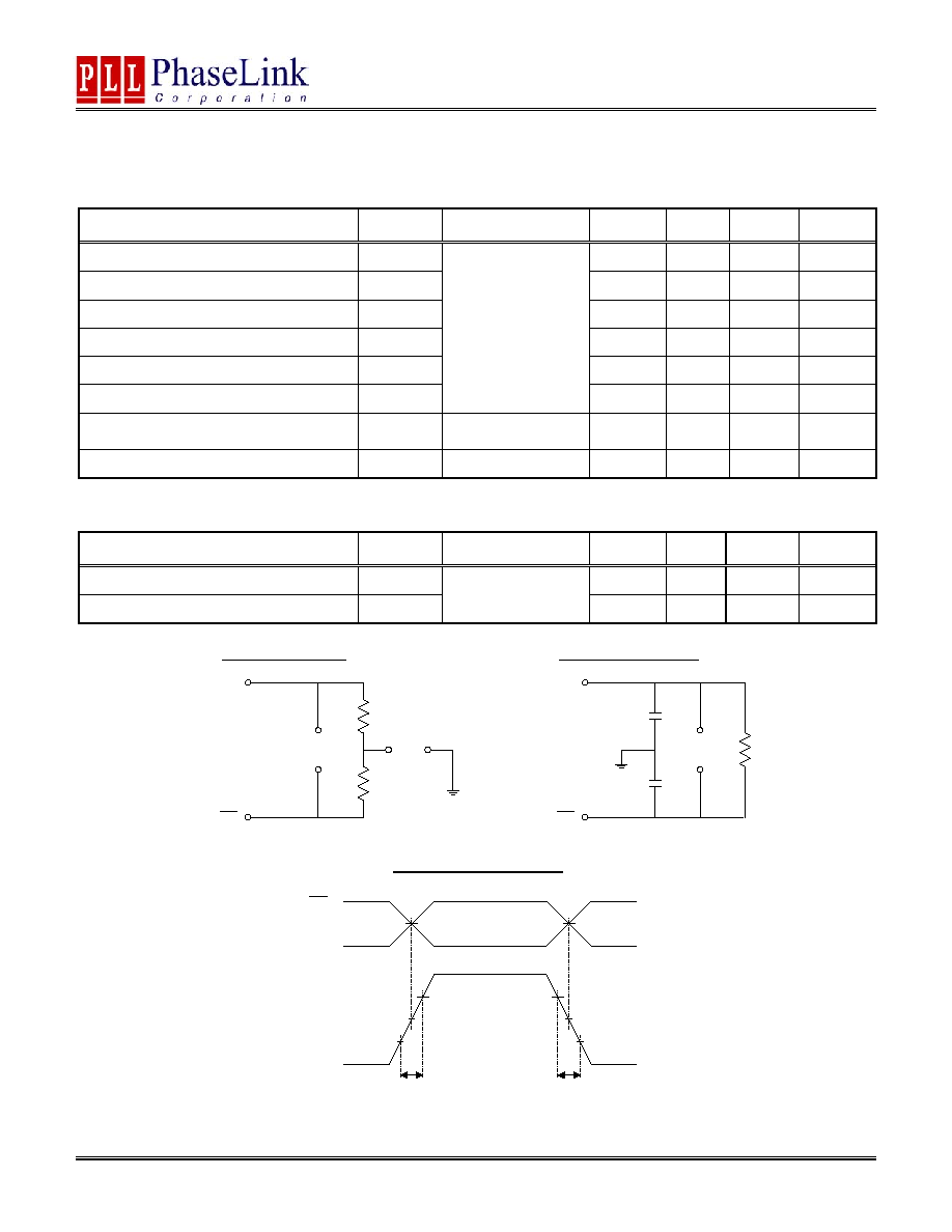
7. LVDS Electrical Characteristics
PARAMETERS SYMBOL
CONDITIONS
MIN.
TYP.
MAX.
UNITS
Output Differential Voltage
V
OD
247
355
454
mV
V
DD
Magnitude Change
V
OD
-50
50 mV
Output High Voltage
V
OH
1.4
1.6
V
Output Low Voltage
V
OL
0.9
1.1
V
Offset Voltage
V
OS
1.125
1.2
1.375
V
Offset Magnitude Change
V
OS
R
L
= 100
(see figure)
0
3 25 mV
Power-off Leakage
I
OXD
V
out
= V
DD
or GND
V
DD
= 0V
±1
±10
uA
Output Short Circuit Current
I
OSD
-5.7 -8
mA
8. LVDS Switching Characteristics
PARAMETERS SYMBOL
CONDITIONS
MIN.
TYP.
MAX.
UNITS
Differential Clock Rise Time
t
r
0.2 0.7 1.0 ns
Differential Clock Fall Time
t
f
R
L
= 100
C
L
= 10 pF
(see figure)
0.2 0.7 1.0 ns
OUT
OUT
V
OD
V
OS
50
50
OUT
V
DIFF
R
L
= 100
C
L
= 10pF
C
L
= 10pF
LVDS Switching Test Circuit
LVDS Levels Test Circuit
LVDS Transistion Time Waveform
OUT
OUT
OUT
0V (Differential)
0V
20%
80%
20%
80%
t
R
t
F
V
DIFF

(Preliminary)
PL580-30
38MHz-640MHz Low Phase Noise VCXO
47745 Fremont Blvd., Fremont, California 94538 Tel (510) 492-0990 Fax (510) 492-0991 www.phaselink.com Rev 11/30/05 Page 8
9. PECL Electrical Characteristics
PARAMETERS SYMBOL CONDITIONS
MIN. MAX.
UNITS
Output High Voltage
V
OH
V
DD
≠ 1.025
V
Output Low Voltage
V
OL
R
L
= 50
to (V
DD
≠ 2V)
(see figure)
V
DD
≠ 1.620
V
11. PECL Switching Characteristics
PARAMETERS SYMBOL
FREQ.
CONDITIONS MIN. TYP. MAX. UNITS
Clock Rise & Fall Times
<150MHz
0.2 0.5 0.7
Clock Rise & Fall Times
>150MHz
<320MHz
0.2 0.4 0.55
Clock Rise & Fall Times
t
r &
t
f
>320MHz
@20/80% - PECL
@80/20% - PECL
0.2 0.3 0.45
ns
11. CMOS Electrical Characteristics
PARAMETERS SYMBOL CONDITIONS MIN.
TYP.
MAX.
UNITS
I
OH
V
OH
= V
DD
-0.4V, V
DD
=3.3V 30 mA
Output drive current
I
OL
V
OL
= 0.4V, V
DD
= 3.3V
30
mA
Output Clock Rise/Fall Time
0.3V ~ 3.0V with 15 pF load
0.7
ns
Output Clock Rise/Fall Time
20%-80% with 50 Load
0.3 ns
OUT
OUT
50
50
PECL Levels Test Circuit
PECL Transistion Time Waveform
OUT
OUT
50%
20%
80%
t
R
t
F
VDD
DUTY CYCLE
45 - 55%
55 - 45%
50%
OUT
OUT
t
SKEW
PECL Output Skew
2.0V
(Preliminary)
PL580-30
38MHz-640MHz Low Phase Noise VCXO
47745 Fremont Blvd., Fremont, California 94538 Tel (510) 492-0990 Fax (510) 492-0991 www.phaselink.com Rev 11/30/05 Page 9
ORDERING INFORMATION
PhaseLink Corporation, reserves the right to make changes in its products or specifications, or both at any time without notice. The information
furnished by Phaselink is believed to be accurate and reliable. However, PhaseLink makes no guarantee or warranty concerning the accuracy of said
information and shall not be responsible for any loss or damage of whatever nature resulting from the use of, or reliance upon this product.
LIFE SUPPORT POLICY: PhaseLink's products are not authorized for use as critical components in life support devices or systems without the
express written approval of the President of PhaseLink Corporation.
For part ordering, please contact our Sales Department:
47745 Fremont Blvd., Fremont, CA 94538, USA
Tel: (510) 492-0990 Fax: (510) 492-0991
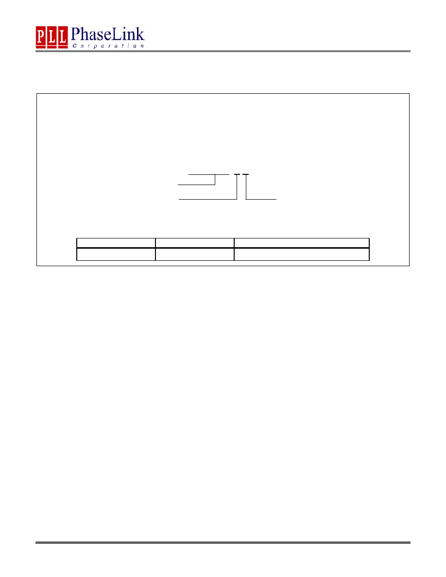
PART NUMBER
The order number for this device is a combination of the following:
Device number, Package type and Operating temperature range
PL580-30
X C
Order Number
Marking
Package Option
PL580-30DC
P580-30DC
Die (Waffle Pack)
PART NUMBER
TEMPERATURE
C=COMMERCIAL
I=INDUSTRAL
PACKAGE TYPE
D= Die