(Preliminary)
PL580-68/69
320-640MHz Low Phase Noise VCXO
47745 Fremont Blvd., Fremont, California 94538 Tel (510) 492-0990 Fax (510) 492-0991 www.phaselink.com Rev 11/28/05 Page 1
FEATURES
∑ Less than 0.4ps RMS (12KHz-20MHz) phase
jitter for
all frequencies
.
∑ Low phase noise output (@ 1MHz frequency
offset
-140dBc/Hz for 320.0MHz,
-131dBC/Hz for 622.08MHz
∑ 20MHz-40MHz crystal input.
∑ 320MHz-640MHz output.
∑ Available in PECL, or LVDS outputs.
∑ No external varicap required.
∑ Output Enable selector.
∑ Wide pull range (+/-200ppm).
∑ 3.3V operation.
∑ Available in 3x3 QFN or 16-pin TSSOP
packages.
DESCRIPTION
The PL580-6X is a monolithic low jitter and low
phase noise VCXO, capable of 0.4ps RMS phase
jitter and PECL or LVDS outputs, covering a wide
frequency output range up to 640MHz. It allows the
control of the output frequency with an input voltage
(VCON), using a low cost crystal.
The PL580-6X is designed to address the
demanding requirements of high performance
applications such as SONET, GPS, Video, etc.
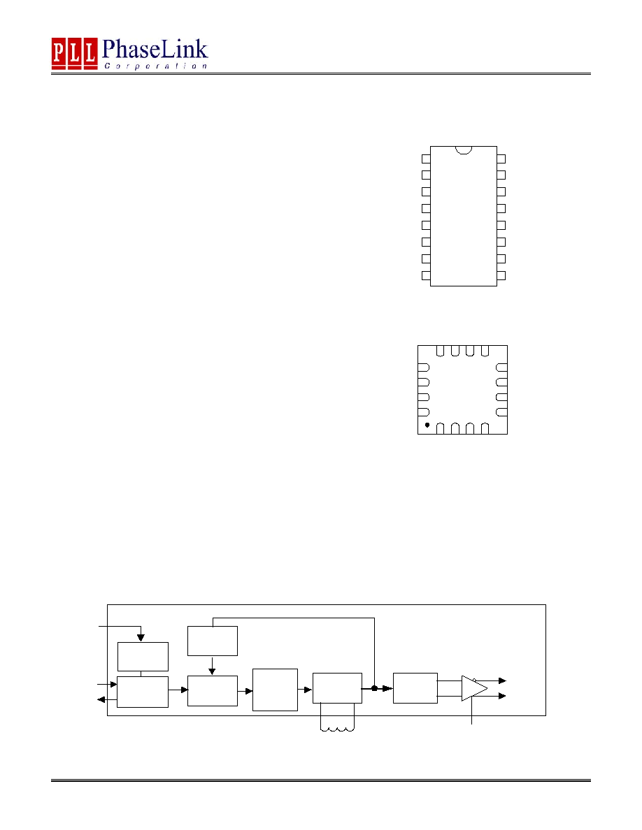
BLOCK DIAGRAM
PACKAGE PIN ASSIGNMENT
Note1: ^ Denotes internal pull up resistor.
Phase
Detector
Charge
Pump
Loop
Filter
VCO
(F
XiN
x16)
VCO
Divider
XTAL
OSC
QBAR
OE
XIN
XOUT
Q
VCON
VARICAP
+
Performance Tuner
Output
Divider
PL5
80-6
X
1
2
3
4
5
6
7
8
VDDANA
9
10
11
12
13
14
15
16
XIN
XOUT
SEL2^
OE_CTRL
VCON
GNDANA
LP
SEL0^
GNDBUF
SEL1^
GNDBUF
QBAR
VDDBUF
Q
LM
PL580-6X
GNDBUF
VDDBUF
Q
QBAR
XI
N
DN
C
DN
C
VDD
A
NA
DNC
XOUT
OE_CTRL
VCON
LP
GN
DA
N
A
LM
GN
D
B
UF
4
16
15
14
13
12
11
10
9
8
7
6
5
1
2
3
(Preliminary)
PL580-68/69
320-640MHz Low Phase Noise VCXO
47745 Fremont Blvd., Fremont, California 94538 Tel (510) 492-0990 Fax (510) 492-0991 www.phaselink.com Rev 11/28/05 Page 2
OUTPUT ENABLE LOGICAL LEVELS
Part #
OE
State
0 (Default)
Output enabled
PLL580-68 (PECL)
1 Tri-state
0 Tri-state
PLL580-69 (LVDS)
1 (Default)
Output enabled
PIN DESCRIPTIONS
Name
TSSOP
Pin number
3x3mm QFN
Pin number
Type Description
VDDANA
1
11
P
VDD for analog Circuitry.
XIN
2
12
I
Crystal input pin. (See Crystal Specifications on page 4).
XOUT
3
13
O
Crystal output pin. (See Crystal Specifications on page 4).
DNC
4
14
-
Do Not Connect
OE_CTRL
5
15
I
Output enable control pin. (See OE_CTRL Logic Levels above).
VCON
6
16
I
Voltage control input.
GNDANA
7
1
P
Ground for analog circuitry.
LP 8 2
-
LM 9 3
-
Tuning inductor connection. The inductor is recommended to be
a high Q small size 0402 or 0603 SMD component, and must be
placed between LP and adjacent LM pin. Place inductor as close
to the IC as possible to minimize parasitic effects and to
maintain inductor Q.
GNDBUF
10
4
P
GND connection for output buffer circuitry.
Q
11
5
O
PECL or LVDS output.
VDDBUF 12
6 P
VDD connection for output buffer circuitry. VDDBUF should be
separately decoupled from other VDDs whenever possible.
QBAR
13
7
O
Complementary PECL, LVDS output.
GNDBUF
14
8
P
GND connection for output buffer circuitry.
DNC
15
9
-
Do Not Connect
DNC
16
10
-
Do Not Connect
(Preliminary)
PL580-68/69
320-640MHz Low Phase Noise VCXO
47745 Fremont Blvd., Fremont, California 94538 Tel (510) 492-0990 Fax (510) 492-0991 www.phaselink.com Rev 11/28/05 Page 3
FREQUENCY SELECTION TABLE
SEL2 SEL1
SEL0
Selected Multiplier/Output Frequency
0 0 0
VCO
Max*
0 0 1
VCO
Min*
1 1 1
Fin
x
16
All Other Combinations
Reserved
All SEL pads have internal pull-ups (default value is `1'). Bond to GND to set to 0.
* Special Test Modes to help selecting the inductor value for the target output frequency.
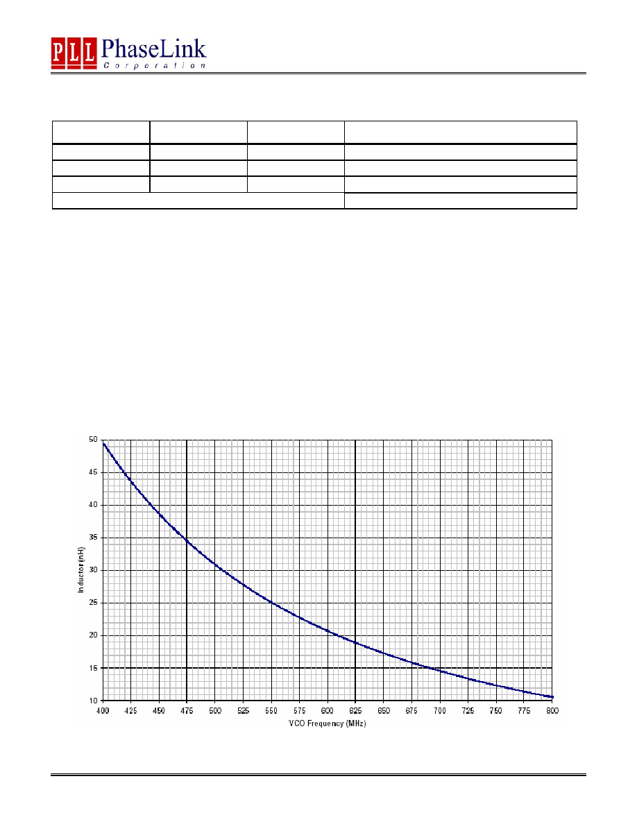
PERFORMANCE TUNING & INDUCTOR VALUE SELECTION
Please refer to PhaseLink's `PhasorV Tuning Assistance' software to automatically calculate the optimum inductor
values for your application. In addition, the chart below could be used as a reference for quick inductor value
selection. Please note that the inductor values mentioned in the table below, or when using `PhasorV Tuning
Assistance' are derived based on the parasitic values of PhaseLink's evaluation board. For performance
enhancement of your custom board design, please follow the following instruction:
Use the special test modes "VCO Max" and "VCO Min" to determine the optimum inductor value. "VCO Max"
represents the high end of the VCO range and "VCO Min" represents the low end of the VCO range. The output
frequency in the "VCO Max" and "VCO Min" test modes is VCO/16. This means that the output frequencies are
around the crystal frequency that will be used. The optimum inductor value is where the target crystal frequency
is closest to the middle between the "VCO Max" and "VCO Min" output frequencies. In this case the VCO will lock
in the middle of its tuning range with maximum margin on either side.
(Preliminary)
PL580-68/69
320-640MHz Low Phase Noise VCXO
47745 Fremont Blvd., Fremont, California 94538 Tel (510) 492-0990 Fax (510) 492-0991 www.phaselink.com Rev 11/28/05 Page 4
ELECTRICAL SPECIFICATIONS
1. Absolute Maximum Ratings
PARAMETERS SYMBOL
MIN.
MAX.
UNITS
Supply Voltage
V
DD
4.6 V
Input Voltage, dc
V
I
-0.5
V
DD
+0.5 V
Output Voltage, dc
V
O
-0.5
V
DD
+0.5 V
Storage Temperature
T
S
-65 150
∞C
Ambient Operating Temperature*
T
A
-40 85
∞C
Junction Temperature
T
J
125
∞C
Lead Temperature (soldering, 10s)
260
∞C
ESD Protection, Human Body Model
2
kV
Exposure of the device under conditions beyond the limits specified by Maximum Ratings for extended periods may cause permanent damage to the
device and affect product reliability. These conditions represent a stress rating only, and functional operations of the device at these or any other
conditions above the operational limits noted in this specification is not implied.
* Note: Operating Temperature is guaranteed by design for all parts (COMMERCIAL and INDUSTRIAL), but tested for COMMERCIAL grade only.
2. Crystal Specifications
PARAMETERS SYMBOL CONDITIONS MIN.
TYP.
MAX.
UNITS
Crystal Resonator Frequency
F
XIN
Parallel Fundamental Mode
20
40
MHz
at VCON = 0V
17.7
at VCON = 1.65V
9.5
Crystal Loading Rating
C
L (xtal)
at VCON = 3.3V
5.4
pF
Crystal Pullability
C
0
/C
1 (xtal)
AT
cut
250
-
Recommended ESR
R
E
AT cut
30
Note: Crystal Loading rating: The listed numbers are for the IC only. Specify the crystal for the value at VCON = 1.65V and add the PCB & package
parasitic. A round number (i.e. 12pF) can be achieved by adding external capacitors. Try to add the same value to XIN and XOUT, and please note,
that frequency pulling and oscillator gain may decrease.
3. Voltage Control Crystal Oscillator
PARAMETERS SYMBOL CONDITIONS MIN.
TYP.
MAX.
UNITS
VCXO Stabilization Time *
T
VCXOSTB
From power valid
10
ms
VCXO Tuning Range
F
XIN
= 20 ≠ 40MHz;
XTAL C
0
/C
1
< 250
0V
VCON 3.3V
500 ppm
CLK output pullability
VCON=1.65V,
±1.65V
±200
ppm
VCXO Tuning Characteristic
150
ppm/V
Pull range linearity
10
%
VCON pin input impedance
60
k
VCON modulation BW
0V
VCON 3.3V, -3dB
25
kHz
Note: Parameters denoted with an asterisk (*) represent nominal characterization data and are not production tested to any specific limits.
(Preliminary)
PL580-68/69
320-640MHz Low Phase Noise VCXO
47745 Fremont Blvd., Fremont, California 94538 Tel (510) 492-0990 Fax (510) 492-0991 www.phaselink.com Rev 11/28/05 Page 5
4. General Electrical Specifications
PARAMETERS SYMBOL
CONDITIONS
MIN. TYP. MAX. UNITS
Supply Current,
Dynamic (with
Loaded Outputs)
I
DD
PECL/LVDS 320MHz<Fout<640MHz
90/70 mA
Operating Voltage
V
DD
2.97 3.63 V
Output Clock
Duty Cycle
@ 50% V
DD
(CMOS)
@ 1.25V (LVDS)
@ V
DD
≠ 1.3V (PECL)
45
45
45
50
50
50
55
55
55
%
Short Circuit
Current
±50
mA
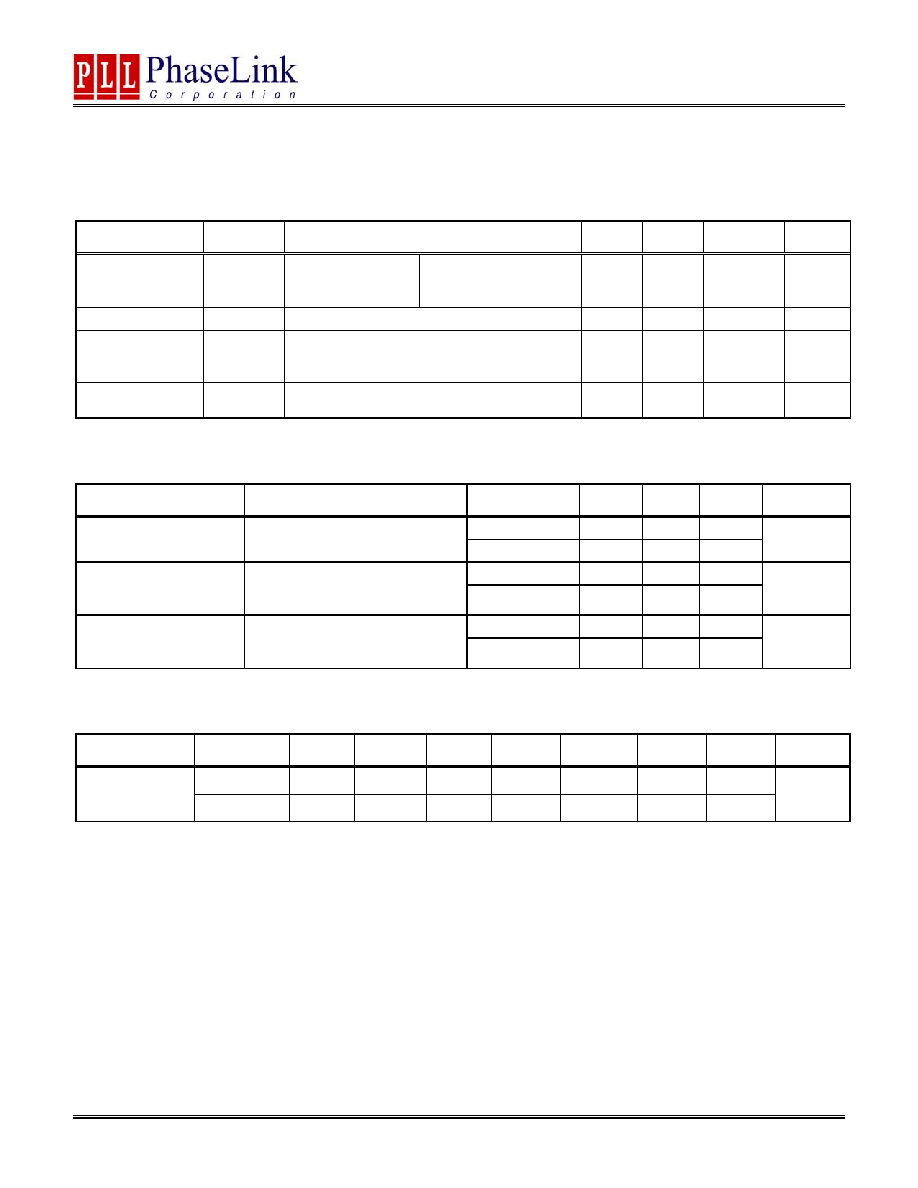
5. Jitter Specifications
PARAMETERS CONDITIONS
FREQUENCY MIN. TYP. MAX. UNITS
320.0MHz 0.4
0.5
Integrated jitter RMS
Integrated 12 kHz to 20 MHz
622.08MHz 0.4
0.6
ps
320.0MHz 3 5
Period jitter RMS
With capacitive decoupling
between VDD and GND.
Over 10,000 cycles.
622.08MHz 6 8
ps
320.0MHz 25
30
Period jitter Peak-to-
Peak
With capacitive decoupling
between VDD and GND.
Over 10,000 cycles.
622.08MHz 40 50
ps
6. Phase Noise Specifications
PARAMETERS FREQ.
@10Hz @100Hz @1kHz @10kHz @100kHz @1M
@10M
UNITS
320.0MHz -59 -86 -116 -129 -124 -140 -148
Phase Noise
2
relative to
carrier (typical)
622.08MHz -48 -80 -108 -118 -114 -131 -138
dBc/Hz