PL611-05
Programmable Quick Turn Clock
T M
47745 Fremont Blvd., Fremont, California 94538 Tel (510) 492-0990 Fax (510) 492-0991 www.phaselink.com Rev 05/05/05 Page 1
FEATURES
∑ Advanced programmable PLL design
∑ Very low Jitter and Phase Noise (30-70ps Pk-Pk typical)
∑ Up to 2 programmable outputs
∑ Output frequency up to 35MHz CMOS.
∑ Accepts Crystal clock input
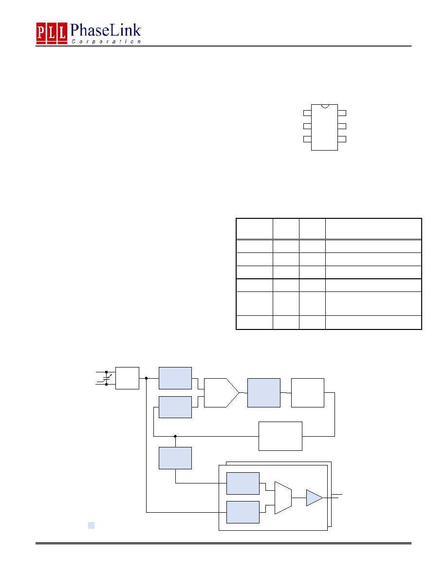
PIN CONFIGURATION
o Fundamental crystal: 10MHz-30MHz
o Reference input: Up to 100MHz
∑ Single 2.5V or 3.3V ± 10% power supply
∑ Operating temperature range from -40∞C to 85∞C
∑ Available in 6-pin SOT Green/RoHS compliant Pkg.
DESCRIPTION
The PL611-05 is a low-cost general purpose
frequency synthesizer and a member of PhaseLink's
Programmable `Quick Turn Clock (QTC)' family.
PhaseLink's PL611-05 offers generating two system
clock frequencies of up to 35MHz form a 10-30MHz
fundamental crystal or a Reference clock source.
Cascading of the ICs to produce additional clock
frequencies is also supported.
PIN DESCRIPTION
Name
Pin
#
Type Description
CLK1
1
O
Programmable Clock Output
GND 2 P
GND
connection
XIN/FIN
3
I
Crystal or Ref. input pin
XOUT
4
O
Crystal output pin
CLK2 5 B
Programmable Clock or
Reference Output
VDD
6
P
VDD connection
BLOCK DIAGRAM
Phase
Detector
Charge
Pump
Loop
Filter
VCO
Selectable
/1,/2,/4,/8
Selectable
/1,/2
Xtal
OSC
XIN/ FIN
XOUT
P-
counter
(
5-
bit)
M
-
counter
(
10-
bit)
R
-
counter
(
8-
bit)
F
Ref
Programmable Function
F
VCO
= F
Ref.
* (2 * M /R)
F
out
= F
VCO
/ (2 * P)
CLK[1:2]
1
2
3
4
5
6
CLK1
GND
XIN/FIN
VDD
XOUT
CLK2
SOT -23
PL611-05
PL611-05
Programmable Quick Turn Clock
T M
47745 Fremont Blvd., Fremont, California 94538 Tel (510) 492-0990 Fax (510) 492-0991 www.phaselink.com Rev 05/05/05 Page 2
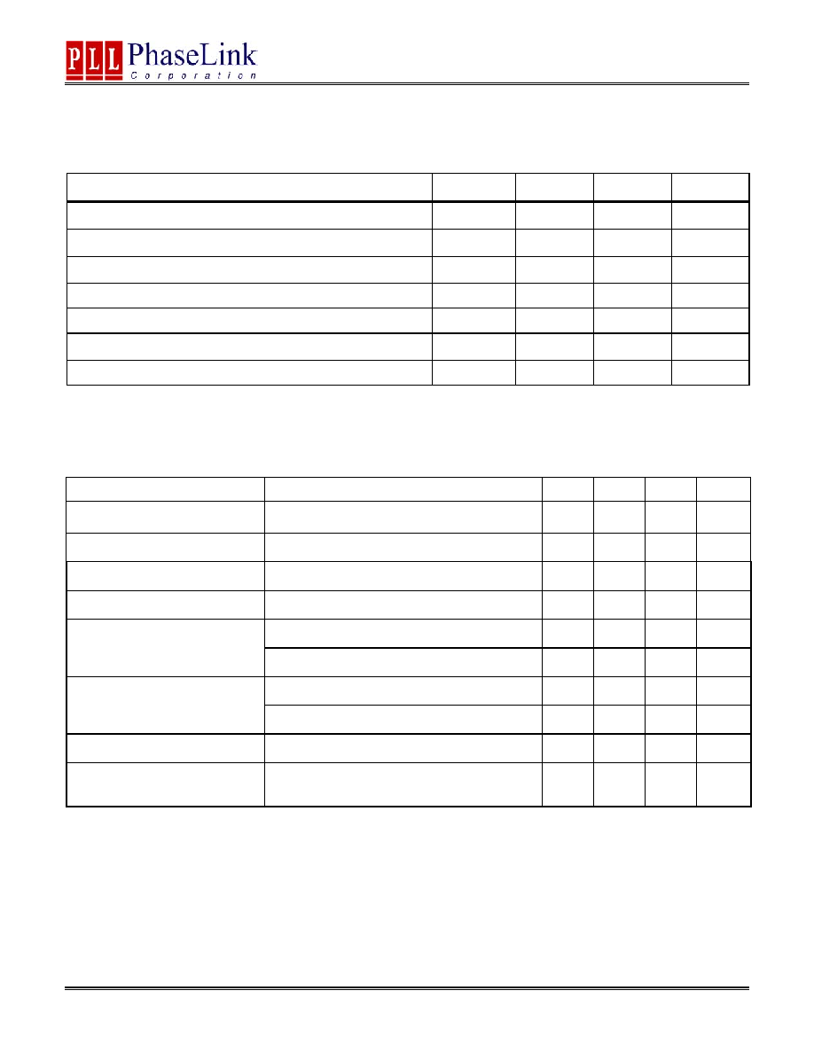
ELECTRICAL SPECIFICATIONS
ABSOLUTE MAXIMUM RATINGS
PARAMETERS SYMBOL
MIN.
MAX.
UNITS
Supply Voltage Range
V
DD
-
0.5
4.6 V
Input Voltage Range
V
I
-
0.5 V
DD
+
0.5
V
Output Voltage Range
V
O
-
0.5 V
DD
+
0.5
V
Soldering Temperature (Green package)
260
∞C
Data Retention @ 85
∞C
10
Year
Storage Temperature
T
S
-65 150
∞C
Ambient Operating Temperature
-40
85
∞C
Exposure of the device under conditions beyond the limits specified by Maximum Ratings for extended periods may cause permanent damage to the device
and affect product reliability. These conditions represent a stress rating only, and functional operations of the device at these or any other conditions above
the operational limits noted in this specification is not implied.
AC SPECIFICATIONS
PARAMETERS CONDITIONS
MIN.
TYP.
MAX.
UNITS
Crystal Input Frequency(XIN)
Fundamental
Crystal
10
30
MHz
Input (FIN) Frequency
100
MHz
Input (FIN) Signal Amplitude
Internally AC coupled
0.9
VDD
Vpp
Settling Time
At power-up (after VDD increases over 1.62V)
10
ms
15pF Load, 10/90%VDD, Standard drive
2.5
3.5
ns
Output Rise Time
15pF Load, 10/90%VDD, High drive
1.0
1.5
ns
15pF Load, 90/10%VDD, Standard drive
2.5
3.5
ns
Output Fall Time
15pF Load, 90/10%VDD, High drive
1.0
1.5
ns
Duty
Cycle
At
VDD/2
45 50 55 %
Period Jitter, peak-to-peak*
(measured from 10,000 samples)
With capacitive decoupling between VDD and
GND. Operating only one output.
70
ps
* Note: Jitter performance depends on the programming parameters.
PL611-05
Programmable Quick Turn Clock
T M
47745 Fremont Blvd., Fremont, California 94538 Tel (510) 492-0990 Fax (510) 492-0991 www.phaselink.com Rev 05/05/05 Page 3
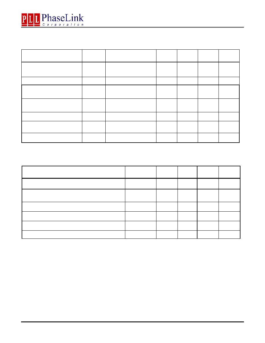
DC SPECIFICATIONS
PARAMETERS SYMBOL
CONDITIONS MIN.
TYP.
MAX.
UNITS
Supply Current, Dynamic, with
Loaded Outputs
I
DD
At 10MHz, load=15pF
15
mA
Operating Voltage
V
DD
2.25 3.63 V
Output Low Voltage
V
OL
I
OL
= +4mA
Standard drive
0.4
V
Output High Voltage
V
OH
I
OH
= -4mA
Standard drive
V
DD
≠
0.4
V
Output Current, Standard drive
I
OSD
V
OL
= 0.4V, V
OH
= 2.4V
10.7
mA
Output Current, High drive
I
OHD
V
OL
= 0.4V, V
OH
= 2.4V
24
mA
Short-circuit Current
I
S
±50
mA
CRYSTAL SPECIFICATIONS
PARAMETERS SYMBOL
MIN.
TYP.
MAX.
UNITS
Fundamental Crystal Resonator Frequency
F
XIN
10 30
MHz
Crystal Loading Rating
(The IC can be programmed for any value in this range.)
C
L (xtal)
5
16*
20 pF
Maximum Sustainable Drive Level
500
µW
Operating Drive Level
100
µW
Crystal Shunt Capacitance
C0
6
pF
Effective Series Resistance, Fundamental, 10-30MHz
ESR
30
Note: C
L
= 16pF is used when not specified. A detailed crystal specification document is also available for this part.
PL611-05
Programmable Quick Turn Clock
T M
47745 Fremont Blvd., Fremont, California 94538 Tel (510) 492-0990 Fax (510) 492-0991 www.phaselink.com Rev 05/05/05 Page 4
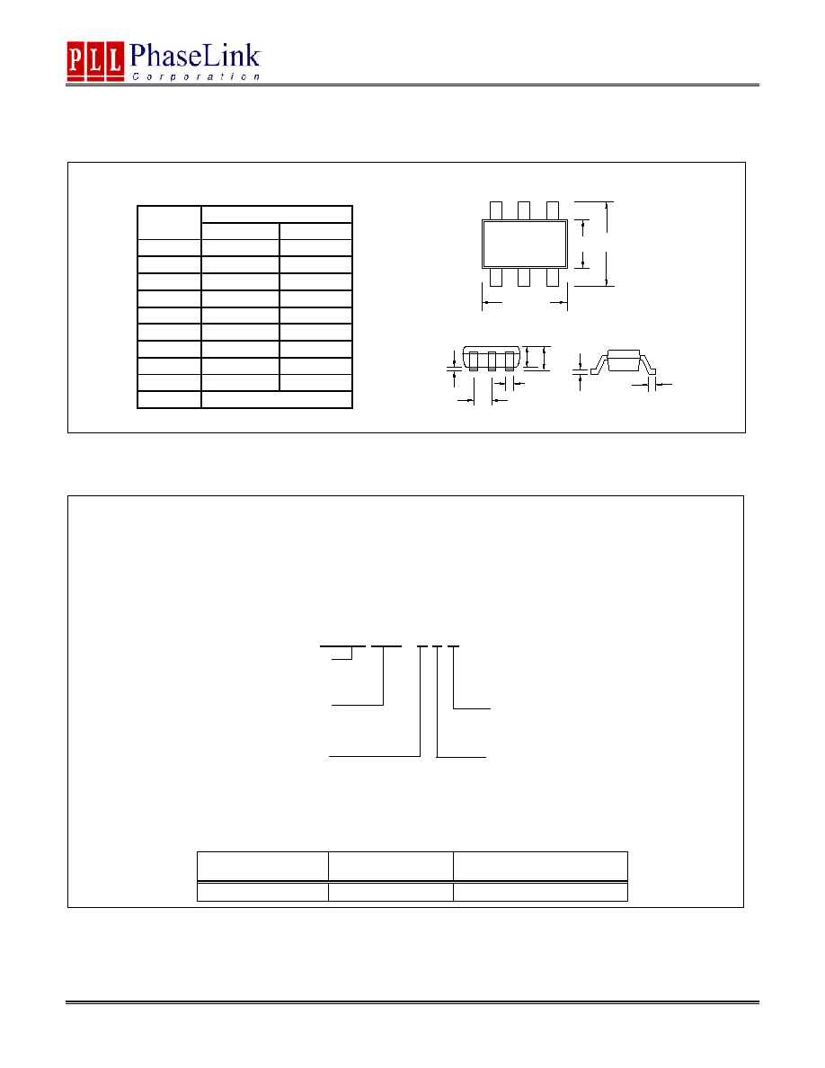
PACKAGE DRAWINGS (GREEN PACKAGE COMPLIANT)
SOT-23 6L
ORDERING INFORMATION
For part ordering, please contact our Sales Department:
47745 Fremont Blvd., Fremont, CA 94538, USA
Tel: (510) 492-0990 Fax: (510) 492-0991
PART NUMBER
The order number for this device is a combination of the following:
Device number, Package type and Operating temperature range
PL611-XXX X X-R
* PhaseLink will assign a unique 3-digit ID code for each approved programmed part number.
* PhaseLink offers Green Package Only for this product family.
Part / Order Number*
Marking
Package Option
PL611-05-XXXTC-R C5XXX
6-Pin SOT-23 (Tape and Reel)
PhaseLink Corporation, reserves the right to make changes in its products or specifications, or both at any time without notice. The information
furnished by Phaselink is believed to be accurate and reliable. However, PhaseLink makes no guarantee or warranty concerning the accuracy of said
information and shall not be responsible for any loss or damage of whatever nature resulting from the use of, or reliance upon this product.
LIFE SUPPORT POLICY: PhaseLink's products are not authorized for use as critical components in life support devices or systems without the
express written approval of the President of PhaseLink Corporation.
Dimension in MM
Symbol
Min. Max.
A 1.05 1.35
A1 0.05 0.15
A2 1.00 1.20
B 0.30 0.50
C 0.08 0.20
D 2.80 3.00
E 1.50 1.70
H 2.60 3.0
L 0.35 0.55
e 0.95
BSC
C
L
A2
E
H
D
A1
e
b
A
PART NUMBER
TEMPERATURE
C=COMMERCIAL
I = INDUSTRIAL
PACKAGE TYPE
T=SOT
3 DIGIT ID Code *
NONE= TUBE
R=TAPE and REEL