PL611-20
Programmable Quick Turn Clock
T M
47745 Fremont Blvd., Fremont, California 94538 Tel (510) 492-0990 Fax (510) 492-0991
Rev 07/06/05 Page 1
FEATURES
∑ Advanced programmable PLL design
∑ Very low Jitter and Phase Noise (< 40ps Pk-Pk typical)
∑ Up to 3 outputs
∑ Output frequency up to 200MHz CMOS.
∑ Crystal inputs:
o Fundamental crystal: 10MHz-30MHz
o 3
RD
overtone crystal: Up to 75MHz
∑ Accepts <1.0V reference signal input voltage
∑ One programmable I/O pin can be configured as
Output Enable (OE), or Frequency Selection input
(FSEL), or Reference clock.
∑ Single 2.5V or 3.3V ± 10% power supply
∑ Operating temperature range from -40∞C to 85∞C
∑ Available in 8-pin MSOP/SOIC, 6-pin SOT Green/
RoHS compliant packages, or Die
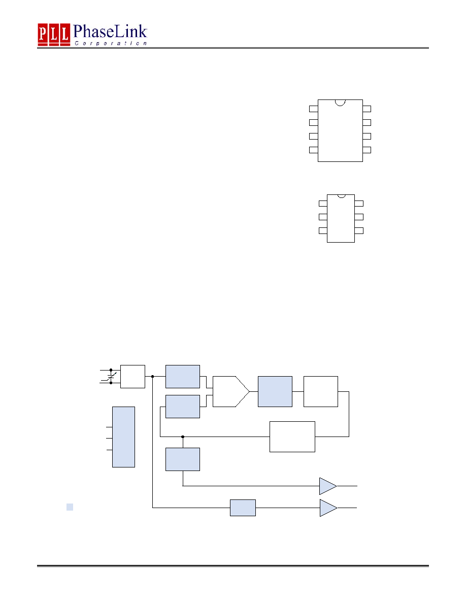
PIN CONFIGURATION
DESCRIPTION
The PL611-20 is a low-cost general purpose frequency synthesizer and a member of PhaseLink's Factory
Programmable `Quick Turn Clock (QTC)' family. PhaseLink's PL611-20 product family can generate any output
frequency up to 200 MHz from fundamental crystal input between 10 MHz - 30 MHz, or a 3rd overtone crystal of
up to 75Mhz.
BLOCK DIAGRAM
Phase
Detector
Charge
Pump
Loop
Filter
VCO
Xtal
OSC
XIN/ FIN
XOUT
P-
counter
(
5-
bit)
M
-
counter
(
10-
bit)
R
-
counter
(
8-
bit)
CLK [0:1]
CLK2, OE, FSEL
F
Ref
OE
FSEL
F
VCO
= F
Ref.
* (2 * M /R)
F
Out
= F
VCO
/ (2 * P)
CLoad
Progra
mmi
ng
Lo
gi
c
Programmable Function
/1, /2
P
L
61
1-
2
0
1
2
3
4
5
6
7
8
XIN/FIN
GND
CLK0
CLK1
XOUT
NC
VDD
CLK2,OE,FSEL
PL
611
-20
1
2
3
4
5
6
CLK1
GND
XIN/FIN
VDD
XOUT
CLK2,OE,FSEL
SOP-8
MSOP-8
SOT-23
P
L
61
1-
2
0
1
2
3
4
5
6
7
8
XIN/FIN
GND
CLK0
CLK1
XOUT
NC
VDD
CLK2,OE,FSEL
PL
611
-20
1
2
3
4
5
6
CLK1
GND
XIN/FIN
VDD
XOUT
CLK2,OE,FSEL
SOP-8
MSOP-8
SOT-23
PL611-20
Programmable Quick Turn Clock
T M
47745 Fremont Blvd., Fremont, California 94538 Tel (510) 492-0990 Fax (510) 492-0991
Rev 07/06/05 Page 2
KEY PROGRAMMING PARAMETERS
CLK[ 0:2 ]
Output Frequency
Output Drive
Strength
Crystal Load
Programmable
Input/Output (pin #7)
Charge-Pump
Current
Fout = FIN * M / (R * P) where
M=10 bit
R = 8 bit
P = 5 bit
1. CLK[0:1] = VCO / 2 * P
2. CLK0 = ~ CLK1
2. CLK[2]= FIN or FIN/2
Std: 10mA
(default)
High: 24mA
+/- 200ppm
tuning.
One output pin can be
configured as
1. CLK2 = FIN or FIN/2
2. FSEL - input
3. OE - input
4 levels of pump
current setting
PIN DESCRIPTION
Pin #
Name
(M)SOP-8 SOT-23
Type Description
XIN/FIN
1
3
I
Crystal or Reference input pin
GND 2
2
P
GND
connection
CLK[0:1]
3,4
1
O
Programmable Clock Output [note:CLK0=CLK1]
VDD
5
6
P
VDD connection (2.25~3.63V)
DNC
6
-
-
Do No Connect
CLK2, OE, FSEL
7
5
B
This programmable I/O pin can be configured as CLK2
(FIN or FIN/2) output, or OE input, or Frequency
Selection (FSEL) input pin. This pin has an internal 60K
pull up resistor.
State OE
FSEL
0
Tristate
CLK[0:1]
Select Freq. `1'
1 (default)
Normal
mode
Select Freq. `2'
XOUT
8
4
O
Crystal output pin
PL611-20
Programmable Quick Turn Clock
T M
47745 Fremont Blvd., Fremont, California 94538 Tel (510) 492-0990 Fax (510) 492-0991
Rev 07/06/05 Page 3
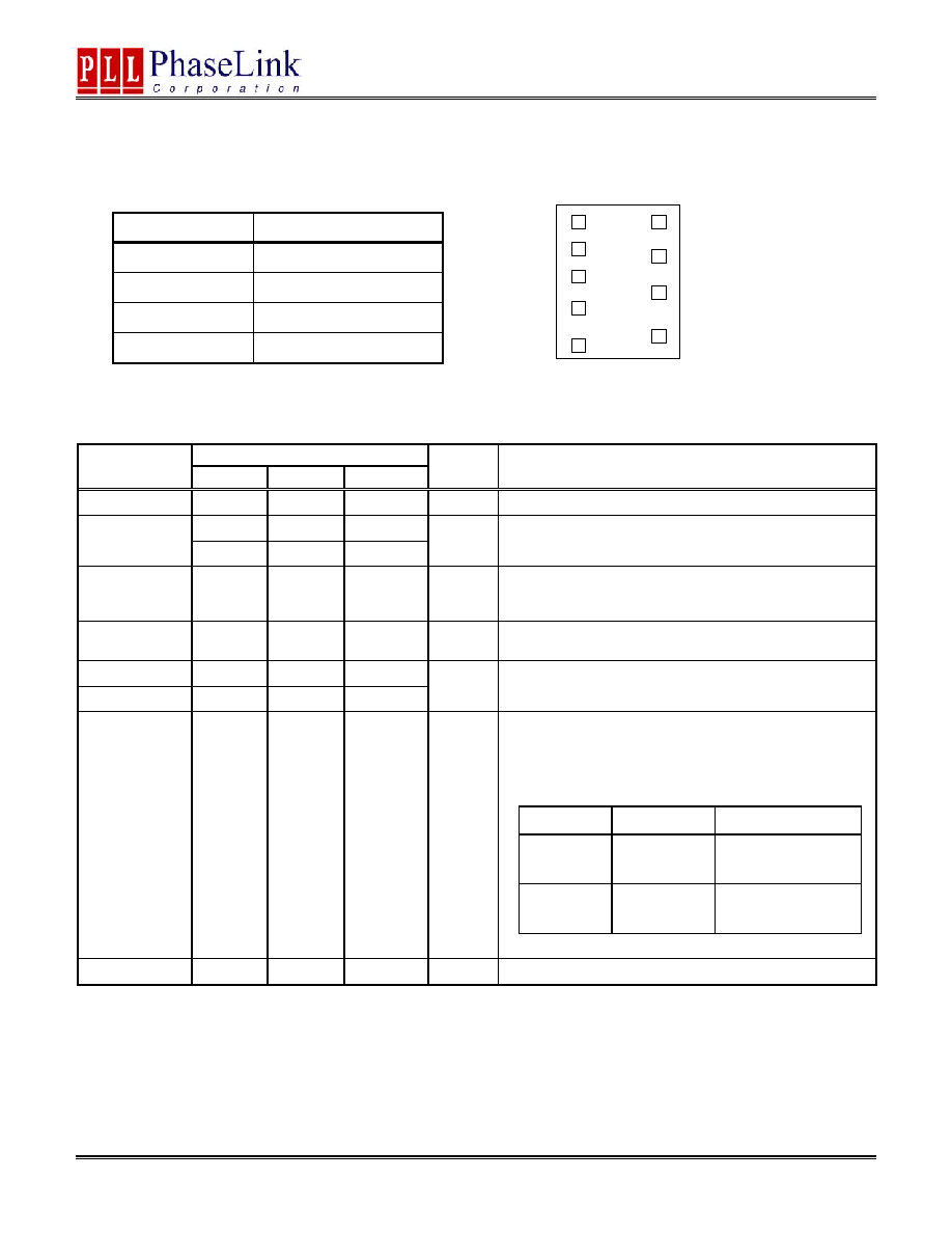
DIE
SPECIFICATION
PAD LAYOUT AND DIE ID
Name Value
Size 31.5x55.1
mil
Reverse side
GND
Pad Opening
80 micron x 80 micron
Die Thickness
10 mil
Note: CLK0=CLK1
PAD ASSIGNMENT and DESCRIPTION
Die Pads
Name
Pad #
X (µm)
Y(µm)
Type Description
XIN 1
101.5
1274.0
I
Crystal
input.
2 101.5
1075.0
GND
3 101.5
878.4
P GND
connection.
CLK0 4
101.5
671.8 O
Optional same frequency clock output (CLK0=CLK1). If the
clock output is not used, the pad should remain as `Do Not
Connect (DNC).
CLK1 5
101.5
425.0 O
Programmable
Clock
Output.
VDD 6
697
483.0
VDD 7
697
790.0
P VDD
connection.
CLK2, OE, FSEL
8 697
1024.0 O
This programmable I/O pin can be configured as CLK2
(FIN or FIN/2) output, or OE input, or Frequency
Selection (FSEL) input pin. This pin has an internal
60K pull up resistor.
State OE
FSEL
0
Tristate
CLK[0:1]
Select Freq. `1'
1 (default)
Normal
mode
Select Freq. `2'
XOUT 9
697
1274.0 O
Crystal
output.
XIN
GND
GND
CLK0
1
2
3
4
5
9
6
7
8
XOUT
CLK2, OE, FSEL
VDD
VDD
1
2
3
4
5
9
6
7
8
CLK1
PL611-20
Programmable Quick Turn Clock
T M
47745 Fremont Blvd., Fremont, California 94538 Tel (510) 492-0990 Fax (510) 492-0991
Rev 07/06/05 Page 4
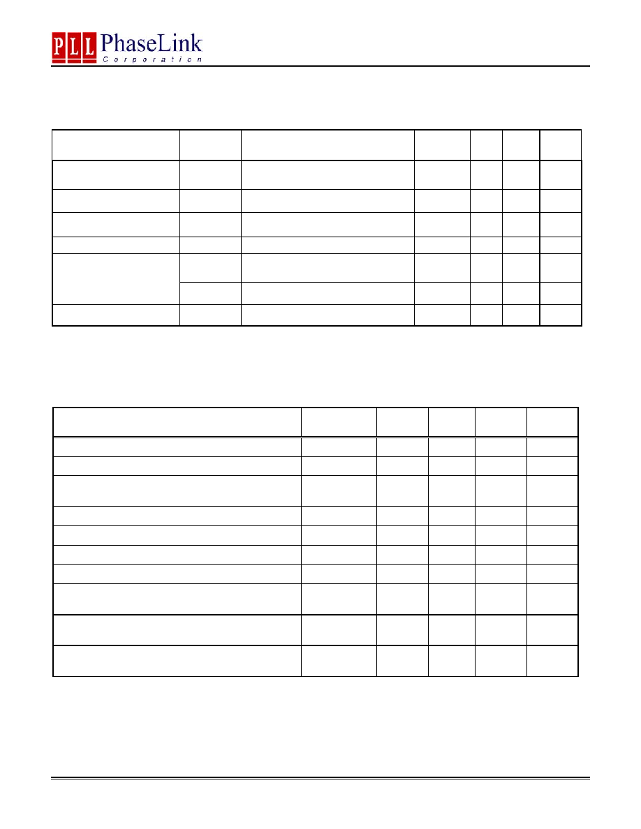
ELECTRICAL SPECIFICATIONS
ABSOLUTE MAXIMUM RATINGS
PARAMETERS SYMBOL
MIN.
MAX.
UNITS
Supply Voltage Range
V
DD
-
0.5
4.6 V
Input Voltage Range
V
I
-
0.5 V
DD
+
0.5
V
Output Voltage Range
V
O
-
0.5 V
DD
+
0.5
V
Data Retention @ 85∫ C
10
Years
Soldering Temperature (Green Package)
260
∞C
Storage Temperature
T
S
-65 150
∞C
Ambient Operating Temperature*
-40
+85
∞C
Exposure of the device under conditions beyond the limits specified by Maximum Ratings for extended periods may cause permanent damage to the device
and affect product reliability. These conditions represent a stress rating only, and functional operations of the device at these or any other conditions above
the operational limits noted in this specification is not implied.
AC SPECIFICATIONS
PARAMETERS CONDITIONS
MIN.
TYP.
MAX.
UNITS
Fundamental Crystal
10
30
MHz
Crystal Input Frequency
3
rd
Overtone Crystal
75
MHz
Settling Time
At power-up (after VDD increases over
1.62V)
10
ms
VDD Sensitivity
Frequency vs. VDD+/-10%
-2
2
ppm
15pF Load, 10/90%VDD, Standard drive
2.5
3.5
ns
Output Rise Time
15pF Load, 10/90%VDD, High drive
1.0
1.5
ns
15pF Load, 90/10%VDD, Standard drive
2.5
3.5
ns
Output Fall Time
15pF Load, 90/10%VDD, High drive
1.0
1.5
ns
Duty Cycle
At VDD/2
45
50
55
%
Max. output skew between
same frequency clocks
Equal loading (15 pF). Equal frequency
& drive strength
200
ps
Period Jitter, peak-to-peak*
(measured from 10,000
samples)
With capacitive decoupling between VDD
and GND. Operating only one output.
40
ps
* Note: Jitter performance depends on the programming parameters.
PL611-20
Programmable Quick Turn Clock
T M
47745 Fremont Blvd., Fremont, California 94538 Tel (510) 492-0990 Fax (510) 492-0991
Rev 07/06/05 Page 5
DC SPECIFICATIONS
PARAMETERS SYMBOL
CONDITIONS
MIN.
TYP.
MAX.
UNITS
Supply Current, Dynamic,
with Loaded Outputs
I
DD
At 10MHz, load=15pF
15
mA
Operating Voltage
V
DD
2.25 3.63 V
Output Low Voltage
V
OL
I
OL
= +4mA (Standard drive)
0.4
V
Output High Voltage
V
OH
I
OH
= -4mA (Standard drive)
V
DD
≠ 0.4
V
I
OSD
V
OL
= 0.4V, V
OH
= 2.4V (Standard
drive)
10 mA
Output Current
I
OHD
V
OL
= 0.4V, V
OH
= 2.4V (High Drive)
24 mA
Short-circuit Current
I
S
±50
mA
CRYSTAL SPECIFICATIONS
PARAMETERS SYMBOL
MIN.
TYP.
MAX.
UNITS
Fundamental Crystal Resonator Frequency
F
XIN
10 30
MHz
3
rd
Overtone Crystal Resonator Frequency
F
XIN
75
MHz
Crystal Loading Rating
(The IC can be programmed for any value in this range.)
C
L (xtal)
5 20 pF
Maximum Sustainable Drive Level
500
µW
Operating Drive Level
100
µW
Crystal Shunt Capacitance
C0
6
pF
Effective Series Resistance, Fundamental, 10-30MHz
R
S
30
Effective Series Resistance, 3
rd
Overtone, 30-50MHz
[CO< 4pF, C
L
=5pF/8pF]
ESR
100/70
Effective Series Resistance, 3
rd
Overtone, 50-65MHz,
[CO< 4pF, C
L
=5pF/8pF]
ESR
60/40
Effective Series Resistance, 3
rd
Overtone, 65-75MHz
[CO< 4pF, C
L
=5pF/8pF
ESR
45/30
Note: A detailed crystal specification document is also available for this part