Preliminary
PLL102-109
Programmable DDR Zero Delay Clock Driver
47745 Fremont Blvd., Fremont, California 94538 TEL (510) 492-0990 FAX (510) 492-0991 Rev 02/26/03 Page 1
FEATURES
∑
PLL clock distribution optimized for Double Data
Rate SDRAM application up to 266Mhz.
∑
Distributes one clock Input to one bank of six
differential outputs.
∑
Track spread spectrum clocking for EMI reduction.
∑
Programmable delay between CLK_INT and CLK[T/C]
from ≠0.8ns to +3.1ns by programming CLKINT and
FBOUT skew channel, or from ≠1.1ns to +3.5ns if
additional DDR skew channels are enabled.
∑
Two independent programmable DDR skew chan-
nels from ≠0.3ns to +0.4ns with step size
±
100ps.
∑
Support 2-wire I
2
C serial bus interface.
∑
2.5V Operating Voltage.
∑
Available in 28-Pin 209mil SSOP.
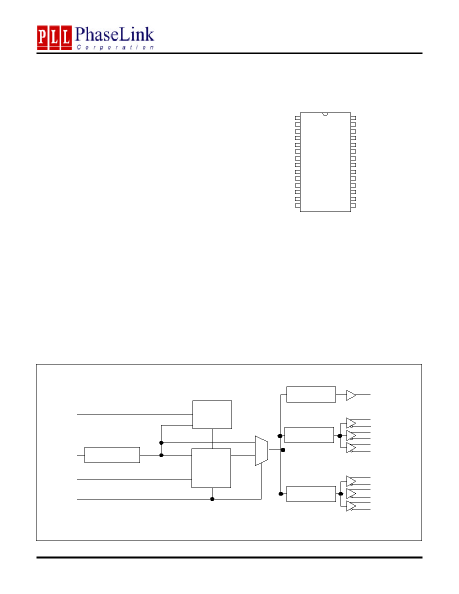
DESCRIPTIONS
The PLL102-109 is a zero delay buffer that distributes
a single-ended clock input to six pairs of differential
clock outputs and one feedback clock output. Output
signal duty cycles are adjusted to 50%, independent of
the duty cycle at CLK_INT. The PLL can be bypassed
for test purposes by strapping AV
DD
to ground.
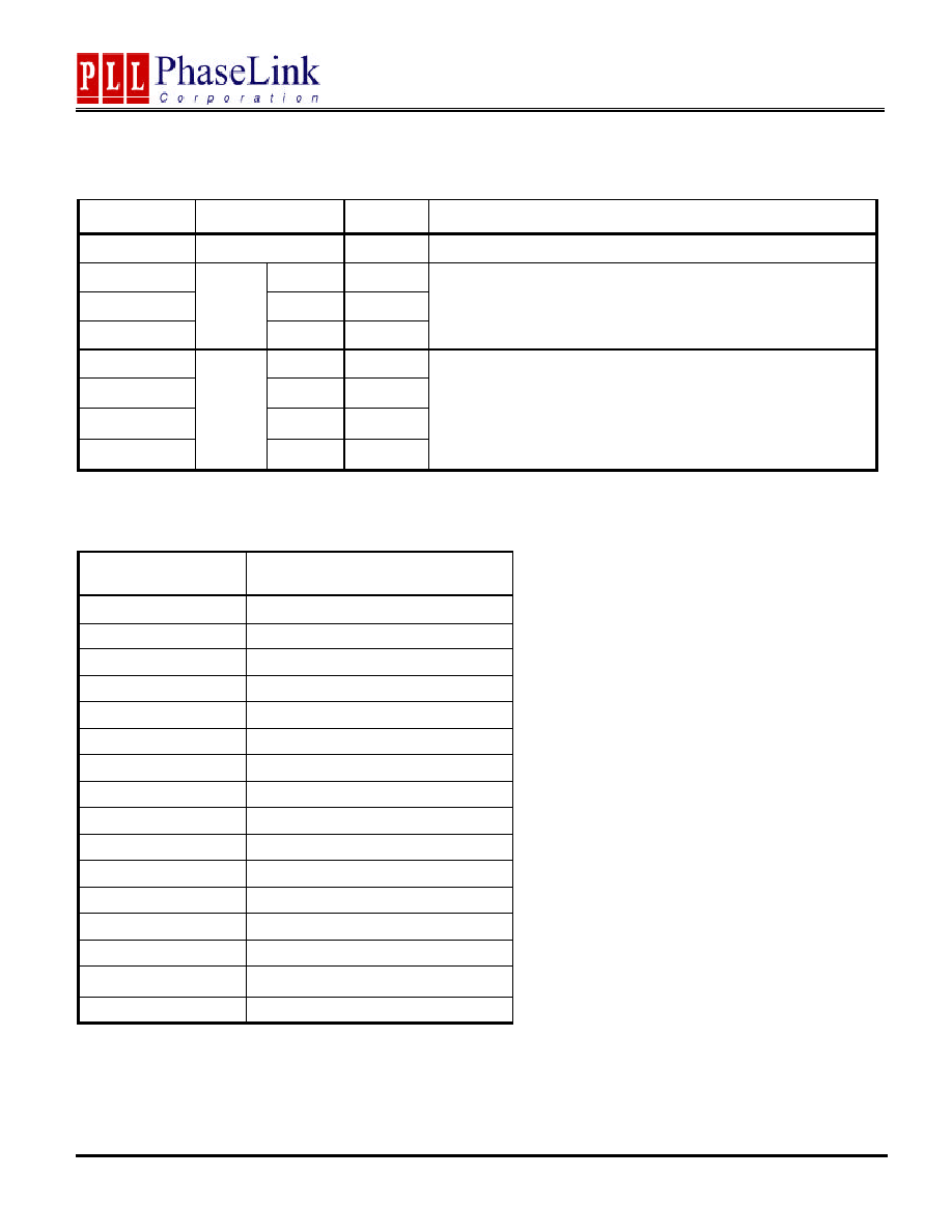
PIN CONFIGURATION
BLOCK DIAGRAM
PLL102-109
CLKC2
VDD
AGND
N/C
CLK_INT
SCLK
CLKC1
CLKT1
VDD
CLKT0
CLKCO
AVDD
SDATA
N/C
FB_INT
FB_OUTT
ADDR_SEL
CLKT3
CLKC3
GND
GND
CLKC5
CLKT5
CLKC4
CLKT4
VDD
1
2
3
4
5
6
7
8
9
10
11
12
13
14
20
19
18
17
16
15
21
22
24
23
25
26
27
28
CLKT2
GND
CLK_INT
FB_INT
Control
Logic
FB_OUTT
CLKT0
CLKC0
CLKT1
CLKC1
CLKT5
CLKC5
CLKT2
CLKC2
CLKT3
CLKC3
CLKT4
CLKC4
AV
DD
AV
DD
-600~+800ps
±200ps step
-300~+400ps
±100ps step
-300~+400ps
±100ps step
(0~2.5ns)
+170ps step
PLL
Programmable
Delay Channel
Programmable
Skew Channel
Preliminary
PLL102-109
Programmable DDR Zero Delay Clock Driver
47745 Fremont Blvd., Fremont, California 94538 TEL (510) 492-0990 FAX (510) 492-0991 Rev 02/26/03 Page 2
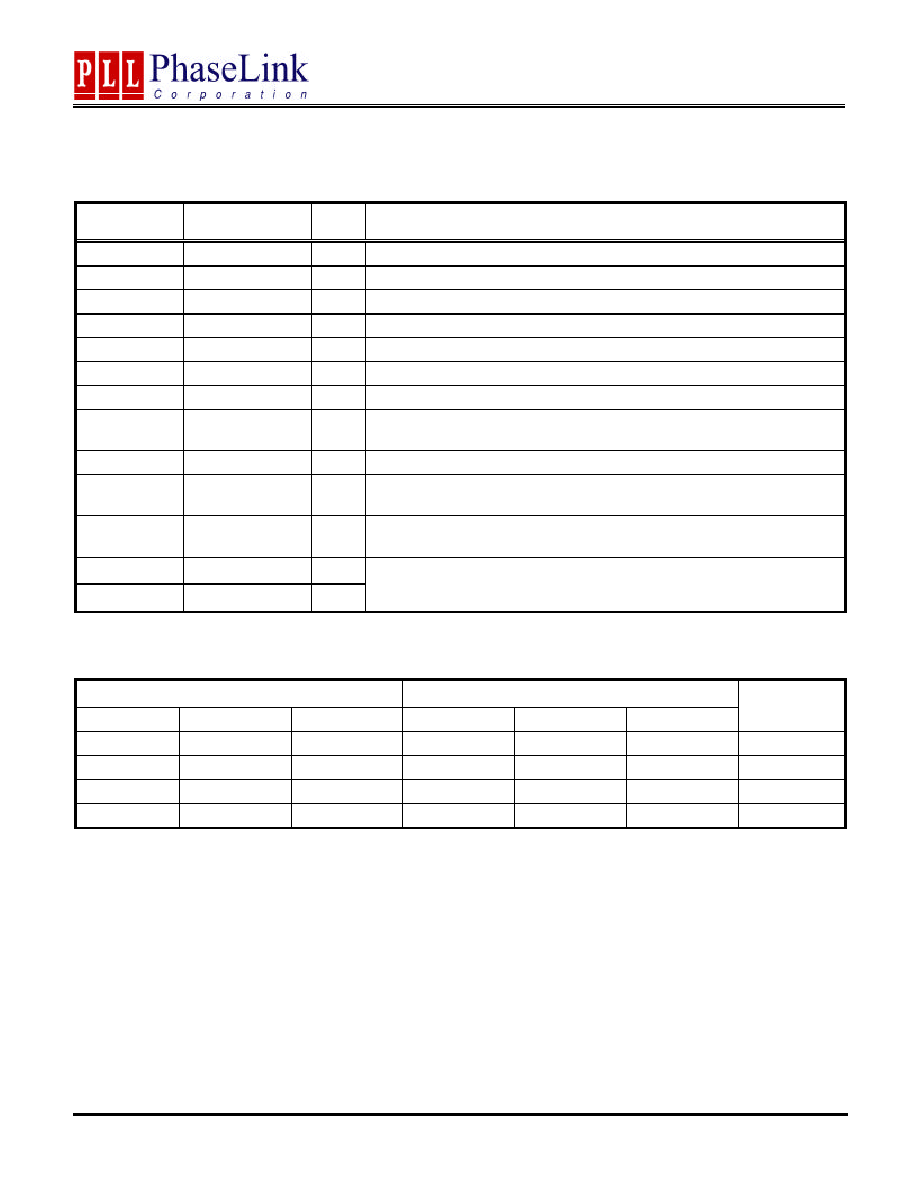
PIN DESCRIPTIONS
Name
Number
Type
Description
VDD
3,12,23
PWR 2.5V power supply.
GND
6,15,28
PWR Ground
AVDD
10
PWR Analog power supply (2.5V).
AGND
11
PWR Analog ground.
CLKT(0:5)
2,4,13,17,24,26
OUT "True" clocks of differential pair outputs.
CLKC(0:5)
1,5,14,16,25,27
OUT "Complementary" clocks of differential pair outputs.
CLK_INT
8
IN
Single-ended 3.3V tolerant input.
ADDR_SEL
18
IN
If ADDR_SEL=0(default) Write condition (0xD4) or a read condition (0xD5)
If ADDR_SEL=1, Write condition (0xD6) or a read condition (0xD7)
N/C
9,21
-
Not connected.
FB_OUTT
19
OUT "True" feedback output. Dedicated for external feedback. It switches at the
same frequency as the CLK_INT.
FB_INT
20
IN
"True" feedback input, provides feedback signal to the internal PLL for
synchronization with CLK_INT to eliminate phase error.
SDATA
22
I/O
SCLK
7
IN
Serial data input for serial interface port.
Functionality
INPUTS
OUTPUTS
AVDD
CLK_INT
CLK_INC
CLKT
CLKC
FB_OUTT
PLL State
2.5V (Nom)
L
H
L
H
L
On
2.5V (Nom)
H
L
H
L
H
On
GND
L
H
L
H
L
Bypass/Off
GND
H
L
H
L
H
Bypass/Off
Preliminary
PLL102-109
Programmable DDR Zero Delay Clock Driver
47745 Fremont Blvd., Fremont, California 94538 TEL (510) 492-0990 FAX (510) 492-0991 Rev 02/26/03 Page 3
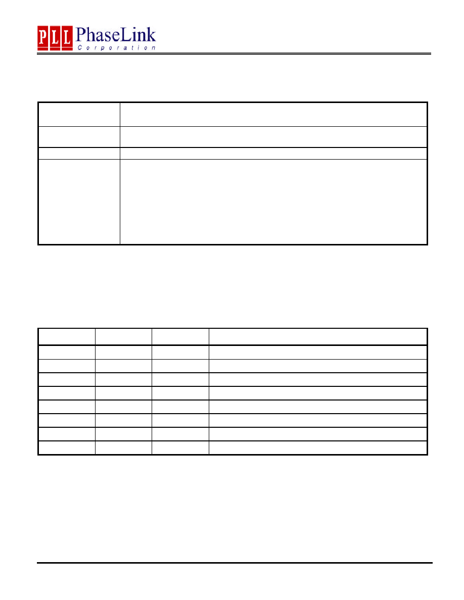
I2C BUS CONFIGURATION SETTING
Address Assignment
A6 A5 A4 A3 A2 A1 A0 R/W
1 1 0 1 0 0 1 _
Slave Re-
ceiver/Transmitter
Provides both slave write and read back functionality
Data Transfer Rate
Standard mode at 100kbits/s
Data Protocol
This serial protocol is designed to allow both blocks write and read from the controller. The
bytes must be accessed in sequential order from lowest to highest byte. Each byte transferred
must be followed by 1 acknowledge bit. A byte transferred without acknowledged bit will termi-
nate the transfer. The write or read block both begins with the master sending a slave address
and a write condition (0xD4) or a read condition (0xD5).
Following the acknowledge of this address byte, in Write Mode: the Command Byte and Byte
Count Byte must be sent by the master but ignored by the slave, in Read Mode: the Byte
Count Byte will be read by the master then all other Data Byte. Byte Count Byte default at
power-up is = (0x09).
I2C CONTROL REGISTERS
1. BYTES 0 TO 4 are reserved power up default =1.
2. BYTE 5: Outputs Register (1=Enable, 0=Disable)
Bit
Pin#
Default
Description
Bit 7
-
-
Reserved
Bit 6
-
-
Reserved
Bit 5
26,27
1
CLKT5, CLKC5 (1= active, 0=inactive)
Bit 4
24,25
1
CLKT4, CLKC4 (1= active, 0=inactive)
Bit 3
16,17
1
CLKT3, CLKC3 (1= active, 0=inactive)
Bit 2
13,14
1
CLKT2, CLKC2 (1= active, 0=inactive)
Bit 1
4,5
1
CLKT1, CLKC1 (1= active, 0=inactive)
Bit 0
1,2
1
CLKT0, CLKC0 (1= active, 0=inactive)
Preliminary
PLL102-109
Programmable DDR Zero Delay Clock Driver
47745 Fremont Blvd., Fremont, California 94538 TEL (510) 492-0990 FAX (510) 492-0991 Rev 02/26/03 Page 4
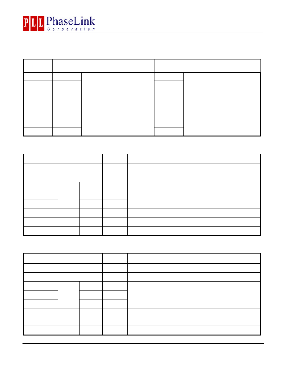
TABLE 1: Output Signals SKEW Programming Summary:
Bit<2:0>
DDR Skew Setting (
±
±
100ps/step)
FBOUT Skew Setting (
±
±
200ps/step)
111
+400ps
+800ps
110
+300ps
+600ps
101
+200ps
+400ps
100
+100ps
+200ps
011
Default
Default
010
-100ps
-200ps
001
-200ps
-400ps
000
-300ps
Setting applies to the following
outputs:
1. DDRA: CLK0, CLK1, CLK5
2. DDRB: CLK2, CLK3, CLK4
.
-600ps
Setting applies to the following out-
puts:
1. FB_OUTT
3. BYTE 6: SKEW Register (1=Enable, 0=Disable)
Bit
Name
Default
Description
Bit 7
-
-
Reserved
Bit 6
-
-
Reserved
Bit 5
Bit <2>
0
Bit 4
Bit <1>
1
Bit 3
Skew
DDRA
Bit <0>
1
These three bits will adjust timing of DDRA signals (CLK0, CLK1,
CLK5) either positive or negative delay up to +400ps or ≠300ps
with
±
100ps per step. (see Table 1)
Bit 2
-
-
-
Reserved
Bit 1
-
-
-
Reserved
Bit 0
-
-
-
Reserved
4. BYTE 7: SKEW Register (1=Enable, 0=Disable)
Bit
Name
Default
Description
Bit 7
DDR-SKEWEN
1
1= disable, 0= enable
Bit 6
FBOUT-SKEWEN
1
1= disable, 0= enable
Bit 5
Bit <2>
0
Bit 4
Bit <1>
1
Bit 3
Skew
DDRC
Bit <0>
1
These three bits will adjust timing of DDRC signals (CLK2, CLK3,
CLK4) either positive or negative delay up to +400ps or ≠300ps
with
±
100ps per step. (see Table 1)
Bit 2
-
-
-
Reserved
Bit 1
-
-
-
Reserved
Bit 0
-
-
-
Reserved
Preliminary
PLL102-109
Programmable DDR Zero Delay Clock Driver
47745 Fremont Blvd., Fremont, California 94538 TEL (510) 492-0990 FAX (510) 492-0991 Rev 02/26/03 Page 5
5. BYTE 8: Outputs Register (1=Enable, 0=Disable)
Bit
Name
Default
Description
Bit 7
-
1
Reserved
Bit 6
Bit <2>
0
Bit 5
Bit <1>
1
Bit 4
Skew
FBOUT
Bit <0>
1
These three bits will adjust timing of FBOUTT signal either positive
or negative delay up to +800ps or ≠600ps with
±
200ps per step.
(see Table 1)
Bit 3
Bit <3>
0
Bit 2
Bit <2>
0
Bit 1
Bit <1>
0
Bit 0
Delay
CLKINT
Bit <0>
0
These four bits will program the propagation delay from CLK_INT
to the input of PLL within the range between 0ps and 2.5ns with
170ps step size. (see Table 2)
TABLE 2: CLK_INT Delay Programming Summary:
Bit<3:0>
CLK_INT to CLK Delay
1111
+2,550 ps
1110
+2,380 ps
1101
+2,210 ps
1100
+2,040 ps
1011
+1,870 ps
1010
+1,700 ps
1001
+1,530 ps
1000
+1,360 ps
0111
+1,190 ps
0110
+1,020 ps
0101
+850 ps
0100
+680 ps
0011
+510 ps
0010
+340 ps
0001
+170 ps
0000
Default

Preliminary
PLL102-109
Programmable DDR Zero Delay Clock Driver
47745 Fremont Blvd., Fremont, California 94538 TEL (510) 492-0990 FAX (510) 492-0991 Rev 02/26/03 Page 6
TABLE 3: Output Drive Strength Programming Summary:
Bit<2:0>
Programming Setting
111
+40%
110
+30%
101
+20%
100
+10%
011
Default
010
-10%
001
-20%
000
-30%
Setting applies to the following outputs
1. DDRA (CLK0, CLK1, CLK5)
2. DDRB (CLK2, CLK3, CLK4)
3.
FBOUT
6. Byte 9: Buffer Drive Strength Control Register
Bit
Name
Default
Description
Bit 7
-
1
Reserved.
Bit 6
-
1
Reserved.
Bit 5
Bit <2>
0
Bit 4
Bit <1>
1
Bit 3
DDRA
Strength
Bit <0>
1
These three bits will program drive strength for CLK0, CLK1 and
CLK5 output clocks (see Table 3).
Bit 2
-
-
-
Reserved
Bit 1
-
-
-
Reserved
Bit 0
-
-
-
Reserved
7. Byte 10: Buffer Drive Strength Control Register
Bit
Name
Default
Description
Bit 7
-
1
Reserved.
Bit 6
-
1
Reserved.
Bit 5
Bit <2>
0
Bit 4
Bit <1>
1
Bit 3
DDRC
Strength
Bit <0>
1
These three bits will program drive strength for CLK2, CLK3 and
CLK4 output clocks (see Table 3).
Bit 2
-
-
-
Reserved
Bit 1
-
-
-
Reserved
Bit 0
-
-
-
Reserved
Preliminary
PLL102-109
Programmable DDR Zero Delay Clock Driver
47745 Fremont Blvd., Fremont, California 94538 TEL (510) 492-0990 FAX (510) 492-0991 Rev 02/26/03 Page 7
8. Byte 11: Buffer Drive Strength Control Register
Bit
Name
Default
Description
Bit 7
-
1
Reserved.
Bit 6
-
1
Reserved.
Bit 5
-
1
Reserved.
Bit 4
-
1
Reserved.
Bit 3
-
1
Reserved.
Bit 2
Bit <2>
0
Bit 1
Bit <1>
1
Bit 0
FBOUTT
Strength
Bit <0>
1
These three bits will program drive strength for FBOUTT output
clock (see Table 3).
Preliminary
PLL102-109
Programmable DDR Zero Delay Clock Driver
47745 Fremont Blvd., Fremont, California 94538 TEL (510) 492-0990 FAX (510) 492-0991 Rev 02/26/03 Page 8
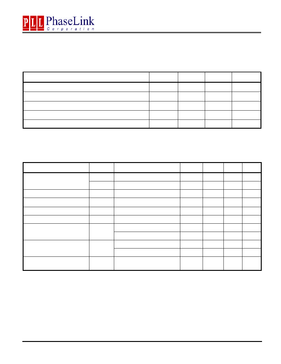
ELECTRICAL SPECIFICATIONS
1. Absolute Maximum Ratings
PARAMETERS
SYMBOL
MIN.
MAX.
UNITS
Supply Voltage Range
V
CC
-
0.5
3.6
V
Input Voltage Range
V
I
-
0.5
V
CC
+
0.5
V
Output Voltage Range
V
O
-
0.5
V
CC
+
0.5
V
Storage Temperature
T
S
-65
150
∞
C
Maximum power dissipation at T
A
= 55
0
C in still air
PW
0.7
W
Exposure of the device under conditions beyond the limits specified by Maximum Ratings for extended periods may cause permanent damage to the
device and affect product reliability. These conditions represent a stress rating only, and functional operations of the device at these or any other con-
ditions above the operational limits noted in this specification is not implied.
2. Electrical Characteristics
PARAMETERS
SYMBOL
CONDITIONS
MIN.
TYP.
MAX. UNITS
I
DD2.5
CL = 0 pF (Fclk=100Mhz)
250
mA
Operating supply current
I
DDPD
CL = 0 pF
100
uA
High Impedance output current
I
OZ
VDD=2.7V, V
OUT
=VDD or GND
±10
uA
Input clamp voltage
V
IK
I
in
= -18mA
-1.2
V
Input Capacitance
C
IN
V
I
= VDD or GND
2
pF
Output Capacitance
C
OUT
V
O
= VDD or GND
3
pF
VDD = Min to Max, I
OH
= -1mA VDD-0.1
V
High level output voltage
V
OH
VDD = 2.3V, I
OH
= -12mA
1.7
V
VDD = Min to Max, I
OL
= 1mA
0.1
V
Low level output voltage
V
OL
VDD = 2.3V, I
OL
= 12mA
0.6
V
Output differential-pair crossing
voltage
V
OC
(VDD/2)-
0.2
(VDD/
2)+0.2
V

Preliminary
PLL102-109
Programmable DDR Zero Delay Clock Driver
47745 Fremont Blvd., Fremont, California 94538 TEL (510) 492-0990 FAX (510) 492-0991 Rev 02/26/03 Page 9
3. Recommended Operating Conditions
PARAMETERS
SYMBOL
MIN.
TYP.
MAX.
UNITS
Output supply voltage
V
CC
2.3
2.5
2.7
V
Analog Supply voltage
A
CC
2.3
2.5
2.7
V
High level input voltage
V
IH
0.7 x V
CC
V
Low level input voltage
V
IL
0.3 x V
CC
V
Operating free-air temperature
T
A
0
70
∞
C
4. Timing requirements
SYMBOL
PARAMETERS
MIN.
MAX.
UNITS
F
CLK
Input clock frequency
66
266
MHz
D
IN
Input clock duty cycle
40
60
%
T
S
Stabilization time after power up
0.1
ms
5. Switching Characteristics
PARAMETERS
SYMBOL
CONDITIONS
MIN.
TYP.
MAX. UNITS
Low to high level propagation
delay time
T
PLH
CLK_INT to any output
0
High to low level propagation
delay time
T
PHL
CLK_INT to any output
0
ns
66MHz
120
Jitter (peak to peak)
T
p-p
100/133/200/266MHz
75
ps
66MHz
110
Jitter (cycle to cycle)
T
cyc-cyc
100/133/200/266MHz
65
ps
Phase error
t
(phase error)
-150
150
Output to output skew
T
oskew
100
Pulse skew
T
pskew
All differential input and output
terminals are terminated with
120
/
16pF
100
ps
66MHz to 100MHz
49.5
50.5
Duty Cycle
D
T
101MHz to 266MHz
49
51
%
Rise time, Fall time
t
r,
t
f
Load = 120
/
16pF
650
800
950
ps
Preliminary
PLL102-109
Programmable DDR Zero Delay Clock Driver
47745 Fremont Blvd., Fremont, California 94538 TEL (510) 492-0990 FAX (510) 492-0991 Rev 02/26/03 Page 10
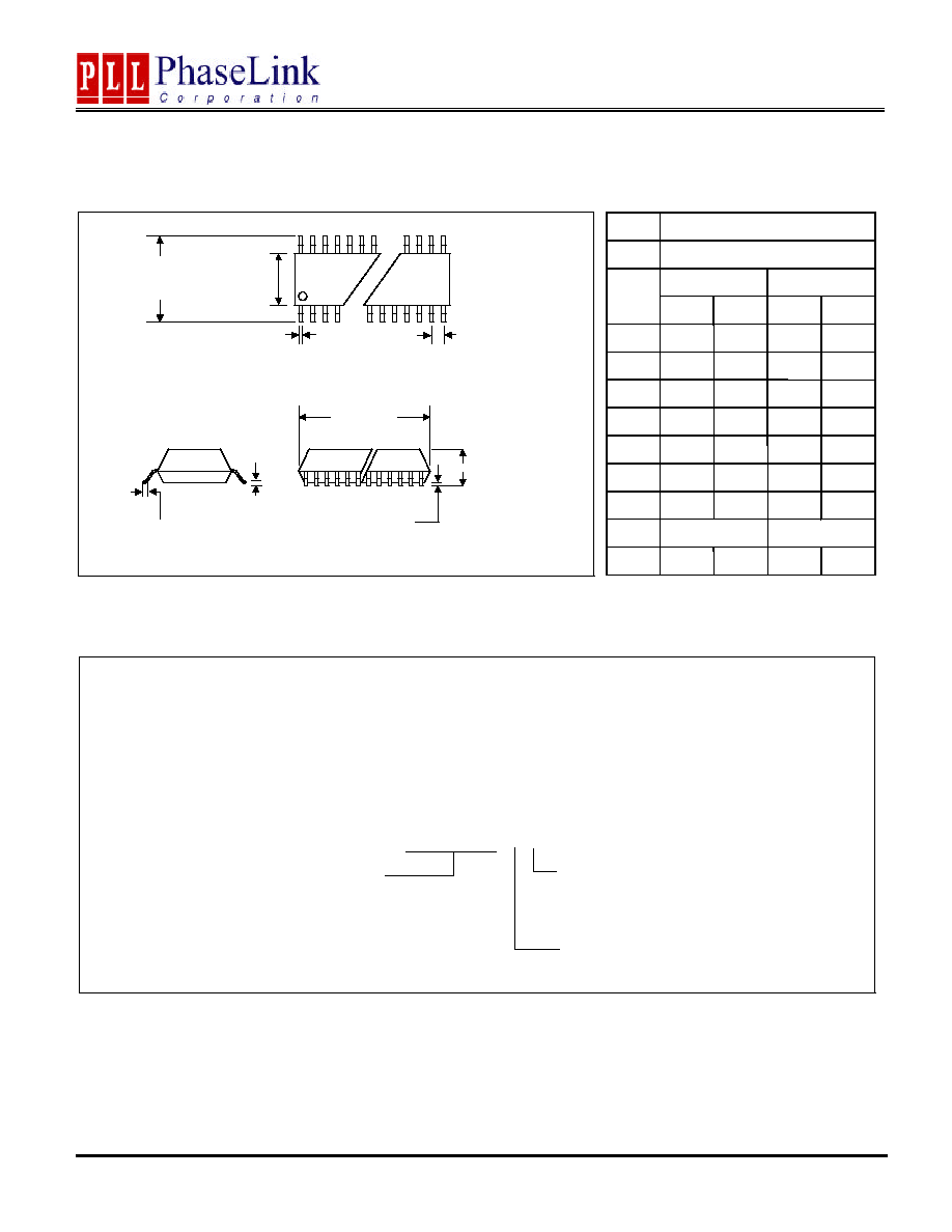
PACKAGE INFORMATION
ORDERING INFORMATION
PhaseLink Corporation, reserves the right to make changes in its products or specifications, or both at any time without notice. The information fur-
nished by Phaselink is believed to be accurate and reliable. However, PhaseLink makes no guarantee or warranty concerning the accuracy of said
information and shall not be responsible for any loss or damage of whatever nature resulting from the use of, or reliance upon this product.
LIFE SUPPORT POLICY: PhaseLink's products are not authorized for use as critical components in life support devices or systems without the ex-
press written approval of the President of PhaseLink Corporation.
For part ordering, please contact our Sales Department:
47745 Fremont Blvd., Fremont, CA 94538, USA
Tel: (510) 492-0990 Fax: (510) 492-0991
PART NUMBER
The order number for this device is a combination of the following:
Device number, Package type and Operating temperature range
PLL102-109 X C
PART NUMBER
TEMPERATURATURE
C=COMMERCIAL
M=MILITARY
I=INDUSTRAL
PACKAGE TYPE
X=SSOP
A1
D
C
L
A
e
E
E1
B
28PIN SSOP
L
0.022
0.038
0.55
0.95
0.220
e
0.65BSC
0.0256BSC
E1
5.00
5.60
0.197
0.413
E
7.40
8.20
0.291
0.323
D
9.9
10.5
0.390
0.015
C
0.09
0.25
0.004
0.010
B
0.25
0.38
0.01
0.079
A1
0.05
0.002
A
2.0
Unit
mm
inches
min
max
min
max
Package
SSOP (QSOP) 209mil
Pins#
28