PLL102-10
Low Skew Output Buffer
47745 Fremont Blvd., Fremont, California 94538 Tel (510) 492-0990 Fax (510) 492-0991 www.phaselink.com Rev 03/22/05 Page 1
FEATURES
∑ Frequency range 50 ~ 120MHz.
∑ Internal phase locked loop will allow spread spec-
trum modulation on reference clock to pass to out-
puts.
∑ Zero input - output delay.
∑ Less than 700 ps device - device skew.
∑ Less than 250 ps skew between outputs.
∑ Less than 100 ps cycle - cycle jitter.
∑ 2.5V or 3.3V power supply operation.
∑ Available in 8-Pin SOIC or MSOP package.
DESCRIPTION
The PLL102-10 is a high performance, low skew, low
jitter zero delay buffer designed to distribute high
speed clocks and is available in 8-pin SOIC or MSOP
package. It has two outputs that are synchronized with
the input. The synchronization is established via
CLKOUT feed back to the input of the PLL. Since the
skew between the input and output is less than
±350
ps, the device acts as a zero delay buffer.
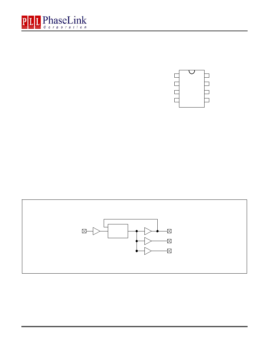
PIN CONFIGURATION
BLOCK DIAGRAM
1
2
3
4
5
6
7
8
REFIN
GND
CLK1
CLK2
CLKOUT
DNC
VDD
DNC
PLL102
-10
PLL
REFIN
CLKOUT
CLK1
CLK2
PLL102-10
Low Skew Output Buffer
47745 Fremont Blvd., Fremont, California 94538 Tel (510) 492-0990 Fax (510) 492-0991 www.phaselink.com Rev 03/17/05 Page 2
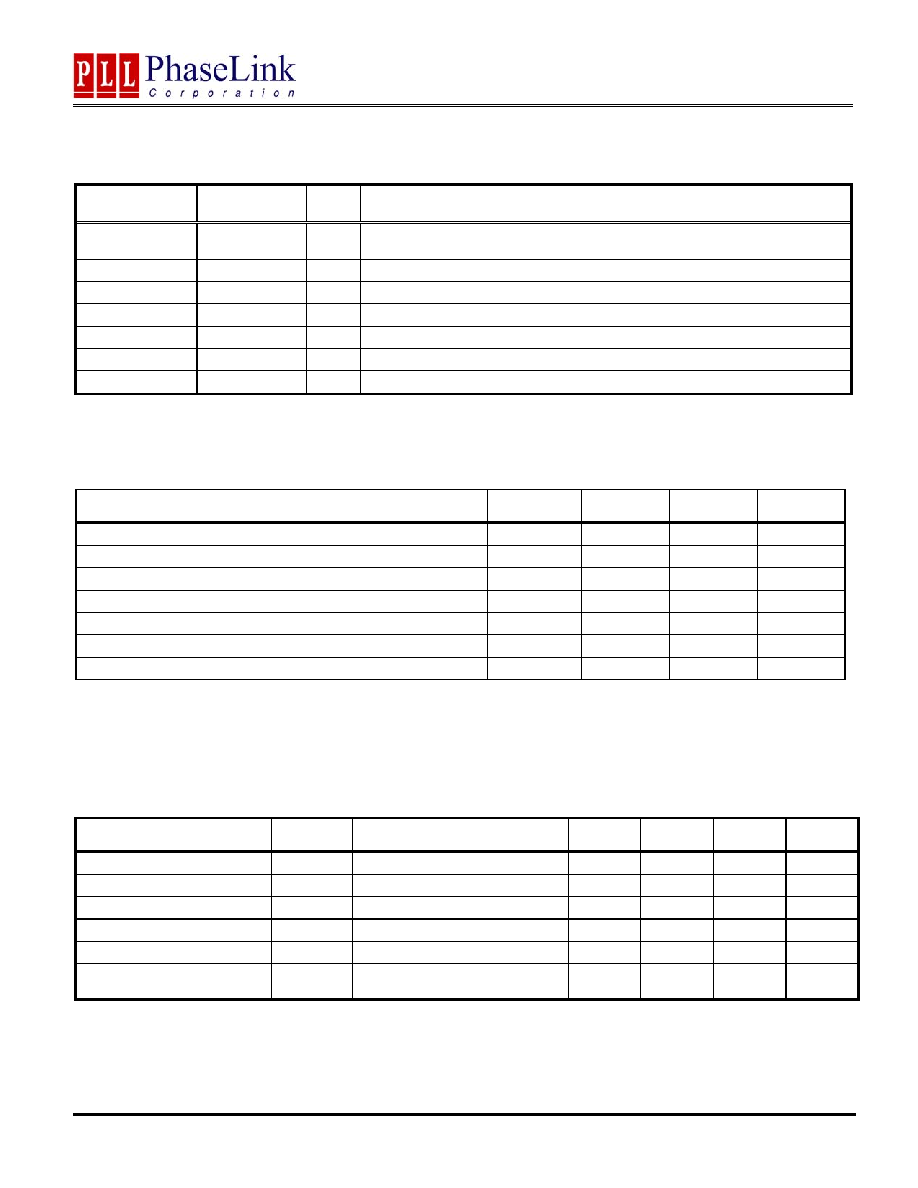
PIN DESCRIPTIONS
Name Number
Type
Description
REFIN 1
I
Input reference frequency. Spread spectrum modulation on this signal will be
passed to the output (up to 100kHz SST modulation).
GND 2
P
Ground
Connection.
CLK1
3
O
Buffered clock output.
CLK2
4
O
Buffered clock output.
VDD
5
P
2.5V or 3.3V Power Supply connection.
DNC
6 & 7
-
Do Not Connect
CLKOUT2
8
O
Buffered clock output. Internal feed back on this pin.
ELECTRICAL SPECIFICATIONS
1. Absolute Maximum Ratings
PARAMETERS SYMBOL
MIN.
MAX.
UNITS
Supply Voltage
V
DD
4.6 V
Input Voltage, dc
V
I
-0.5
V
DD
+0.5 V
Output Voltage, dc
V
O
-0.5
V
DD
+0.5 V
Storage Temperature
T
S
-65 150
∞C
Ambient Operating Temperature*
T
A
-40 85
∞C
Junction Temperature
T
J
125
∞C
Lead Temperature (soldering, 10s)
260
∞C
Exposure of the device under conditions beyond the limits specified by Maximum Ratings for extended periods may cause permanent damage to the
device and affect product reliability. These conditions represent a stress rating only, and functional operations of the device at these or any other con-
ditions above the operational limits noted in this specification is not implied.
* Note: Operating Temperature is guaranteed by design for all parts (COMMERCIAL and INDUSTRIAL), but tested for COMMERCIAL grade only.
2. Electrical Characteristics
PARAMETERS SYMBOL CONDITIONS
MIN.
TYP.
MAX.
UNITS
Supply Voltage
V
DD
2.25
3.63
V
Input Low Voltage
V
IL
0.8
V
Input High Voltage
V
IH
2.0
V
Output Low Voltage
V
OL
I
OL
= 24mA
0.4
V
Output High Voltage
V
OH
I
OH
= 24mA
2.4
V
Supply Current
I
DD
Unloaded outputs at 100MHz,
VDD=3.3V.
22 30
mA

PLL102-10
Low Skew Output Buffer
47745 Fremont Blvd., Fremont, California 94538 Tel (510) 492-0990 Fax (510) 492-0991 www.phaselink.com Rev 03/17/05 Page 3
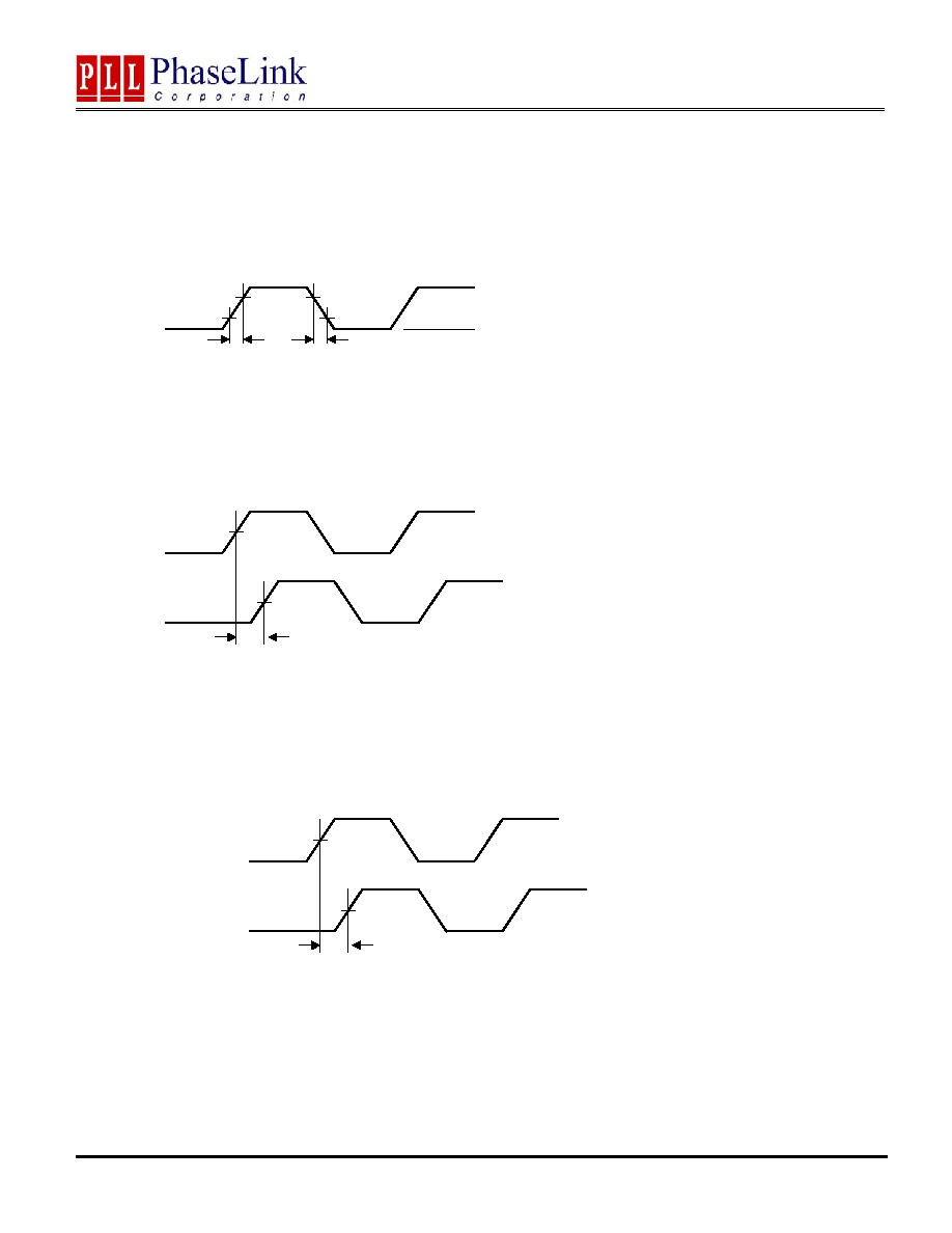
3. Switching Characteristics
PARAMETERS SYMBOL DESCRIPTION
MIN. TYP. MAX.
UNITS
Output Frequency
t1
50
120
MHz
Duty Cycle
DC
Measured at VDD/2,
C
L
=15pF, F
out
= 100MHz
45 50 55 %
Rise Time
T
r
Measured between 10%
and 90%VDD, C
L
=15pF
1.2
1.5 ns
Fall Time
T
f
Measured between 90%
and 10%, C
L
=15pF
1.2
1.5 ns
Output to Output Skew
T
skew
All outputs equally loaded,
C
L
=15pF
250
ps
Delay, REF Rising Edge to
CLKOUT Rising Edge
T
delay
Measured at VDD/2
0
±350
ps
Device to Device Skew
T
dsk-dsk
Measured at V
DD
/2 on the
CLKOUT pins of devices
0
700
ps
Cycle to Cycle Jitter
T
cyc-cyc
Measured at 100MHz
60
ps peak
PLL Lock Time
T
lock
Stable power supply, valid
clock presented on REF pin
1.0
ms
Jitter; Absolute Jitter
T
jabs
At 10,000 cycles, low jitter
input signal
20 50 ps
Jitter; 1-sigma
T
j1-s
At 10,000 cycles, low jitter
input signal
9 15
ps
SWITCHING WAVEFORMS
Duty Cycle Timing
t1
t2
VDD/2
VDD/2
VDD/2
Output - Output Skew
VDD/2
VDD/2
T
SKEW
Output
Output
PLL102-10
Low Skew Output Buffer
47745 Fremont Blvd., Fremont, California 94538 Tel (510) 492-0990 Fax (510) 492-0991 www.phaselink.com Rev 03/17/05 Page 4
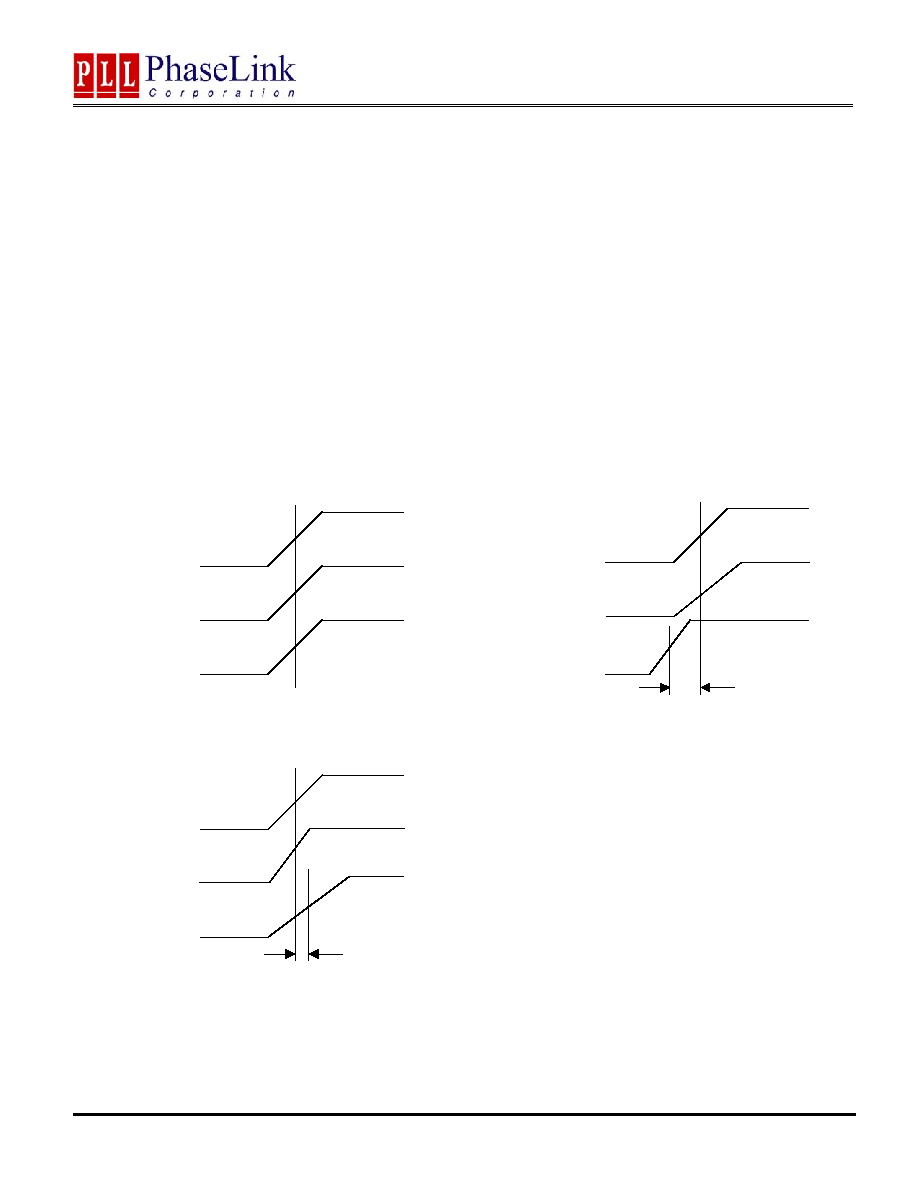
SWITCHING WAVE FORMS
All Outputs Rise/Fall Time
0.8V
2.0V
Output
t
r
t
f
2.0V
0.8V
3.3V
0V
Input to Output Propagation Delay
Input
Output
VDD/2
T
delay
VDD/2
Device to Device Skew
Device1 CLKOUT
Device2 CLKOUT
VDD/2
T
dsk - dsk
VDD/2
PLL102-10
Low Skew Output Buffer
47745 Fremont Blvd., Fremont, California 94538 Tel (510) 492-0990 Fax (510) 492-0991 www.phaselink.com Rev 03/17/05 Page 5
Output-Output Skew
REF
CLKOUT
The skew between CLKOUT and the CLK(1-2) outputs is not dynamically adjusted by the
PLL. Since CLKOUT is one of the inputs to the PLL, zero phase difference is maintained
from REF to CLKOUT. If all outputs are equally loaded, zero phase difference will be
maintained from REF to all outputs.
If applications requiring zero output-output skew, all the outputs must be equally loaded.
If the CLK(1-2) outputs are less loaded than CLKOUT, CLK(1-2) outputs will lead it; if the
CLK(1-2) is more loaded than CLKOUT, CLK(1-2) will lag the CLKOUT.
Since the CLKOUT and the CLK(1-2) outputs are identical, they all start at the same time,
but difference loads cause them to have different rise times and different times crossing
the measurement thresholds.
CLK(1-2)
Zero Delay
REF
CLKOUT
CLK(1-2)
Advanced
REF
CLKOUT
CLK(1-2)
Delayed
REF input and all outputs are equally loaded
REF input and CLK(1-2) outputs are equally loaded,
with CLK(1-2) less loaded than CLKOUT.
REF input and CLK(1-2) outputs loaded equally,
withCLK(1-2) more loaded then CLKOUT.