PLL103-02 Rev.D
DDR SDRAM Buffer for Desktop PCs with 4 DDR DIMMS
47745 Fremont Blvd., Fremont, California 94538 TEL (510) 492-0990 FAX (510) 492-0991 Rev 01/11/01 Page 1
FEATURES
∑
Generates 24 output buffer from one input.
∑
Supports up to four DDR DIMMS.
∑
Supports 266MHz DDR SDRAM.
∑
One additional output for feedback.
∑
Less than 5ns delay.
∑
Skew between any outputs is less than 100 ps.
∑
2.5V Supply range.
∑
Enhanced DDR Output Drive selected by I2C.
∑
Available in 48 pin SSOP.
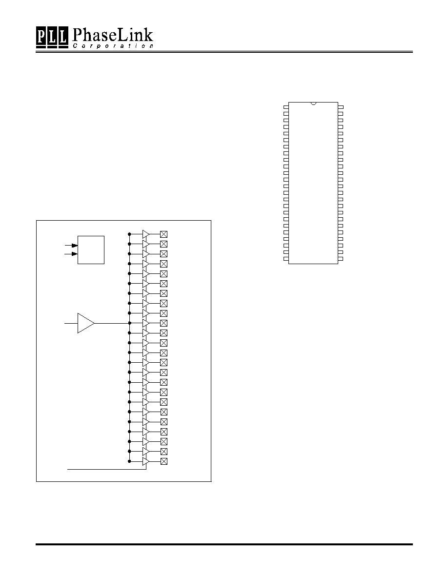
BLOCK DIAGRAM
PIN CONFIGURATION
Note: #: Active Low
DESCRIPTIONS
The PLL103-02 Rev.D is designed as a 2.5V buffer
to distribute high-speed clocks in PC applications.
The device has 24 outputs. These outputs can be
configured to support four unbuffered DDR DIMMS.
The PLL103-02 Rev.D can be used in conjunction
with the PLL202-04 or similar clock synthesizer for
the VIA Pro 266 chipset.
The PLL103-02 Rev.D also has an I2C interface,
which can enable or disable each output clock.
When power up, all output clocks are enabled (has
internal pull up).
PLL103-02
DDR5C
DDR4C
DDR4T
GND
VDD2.5
DDR3C
DDR3T
GND
VDD2.5
DDR2C
GND
VDD2.5
DDR1C
DDR0C
DDR0T
GND
VDD2.5
FBOUT
SDATA
VDD2.5
DDR5T
DDR2T
DDR10C
VDD2.5
GND
DDR9T
DDR9C
VDD2.5
PD#
GND
DDR8T
DDR8C
VDD2.5
N/C
VDD2.5
GND
DDR11T
DDR11C
DDR10T
GND
DDR6T
DDR7T
DDR7C
GND
SCLK
1
2
3
4
5
6
7
8
9
10
11
12
13
14
15
16
17
18
19
20
21
22
23
24
40
39
38
37
36
35
34
33
32
31
30
29
28
27
26
25
41
42
44
43
45
46
47
48
BUF_IN
DDR1T
DDR6C
BUF_IN
SDATA
SCLK
I2C
Control
PD#
DDR0T
DDR0C
DDR1T
DDR1C
DDR2T
DDR2C
DDR3T
DDR3C
DDR4T
DDR4C
DDR5T
DDR5C
DDR6T
DDR6C
DDR7T
DDR7C
DDR8T
DDR8C
DDR9T
DDR9C
DDR10T
DDR10C
DDR11T
DDR11C
PLL103-02 Rev.D
DDR SDRAM Buffer for Desktop PCs with 4 DDR DIMMS
47745 Fremont Blvd., Fremont, California 94538 TEL (510) 492-0990 FAX (510) 492-0991 Rev 01/11/01 Page 2
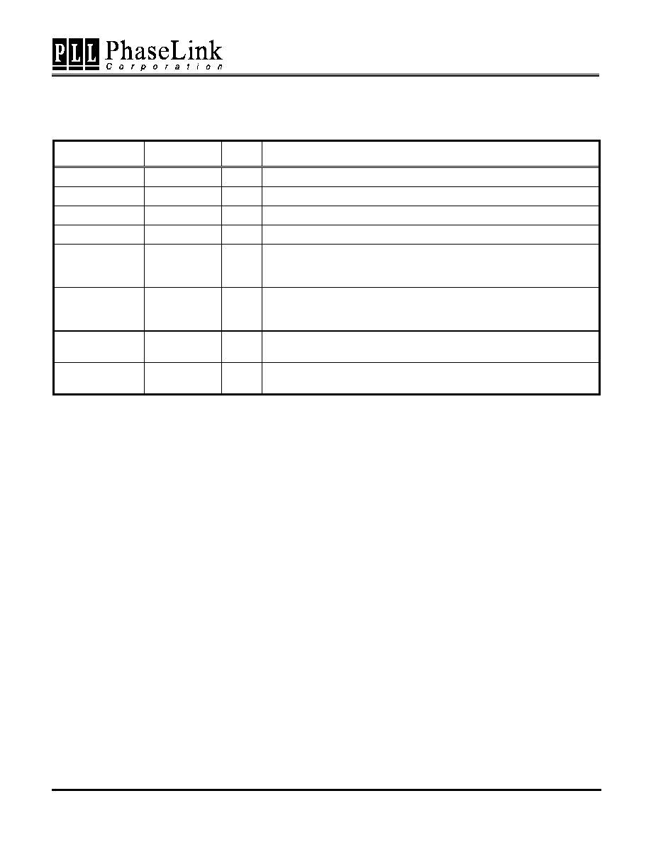
PIN DESCRIPTIONS
Name
Number
Type
Description
FBOUT
1
O
Feedback clock for chipset.
BUF_IN
13
I
Reference input from chipset.
PD
36
I
Power Down Control input. When low, it will tri-state all outputs.
N/C
48
Not connected.
DDR[0:11]T
4,6,10,15,19,
21,28,30,34,
39,43,45
O
These outputs provide True copies of BUF_IN.
DDR[0:11]C
5,7,11,16,20,
22,27,29,33,
38,42,44
O
These outputs provide complementary copies of BUF_IN.
VDD2.5
2,8,12,17,23,
32,37,41,47
P
2.5V power supply.
GND
3,9,14,18,26,
31,35,40,46
P
Ground.
PLL103-02 Rev.D
DDR SDRAM Buffer for Desktop PCs with 4 DDR DIMMS
47745 Fremont Blvd., Fremont, California 94538 TEL (510) 492-0990 FAX (510) 492-0991 Rev 01/11/01 Page 3
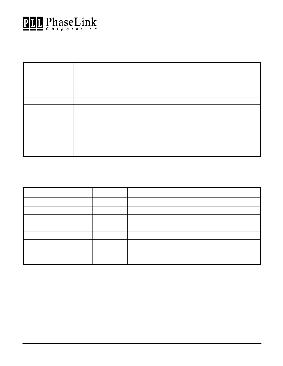
I2C BUS CONFIGURATION SETTING
Address Assignment
A6 A5 A4 A3 A2 A1 A0 R/W
1 1 0 1 0 0 1 _
Slave
Receiver/Transmitter
Provides both slave write and readback functionality
Data Transfer Rate
Standard mode at 100kbits/s
Data Protocol
This serial protocol is designed to allow both blocks write and read from the controller. The
bytes must be accessed in sequential order from lowest to highest byte. Each byte transferred
must be followed by 1 acknowledge bit. A byte transferred without acknowledged bit will
terminate the transfer. The write or read block both begins with the master sending a slave
address and a write condition (0xD2) or a read condition (0xD3).
Following the acknowledge of this address byte, in
Write Mode: the Command Byte and Byte
Count Byte must be sent by the master but ignored by the slave, in Read Mode: the Byte
Count Byte will be read by the master then all other Data Byte. Byte Count Byte default at
power-up is = (0x09).
I2C CONTROL REGISTERS
1. BYTE 6: Outputs Register (1=Enable, 0=Disable)
Bit
Pin#
Default
Description
Bit 7
48
1
Reserved
Bit 6
-
0
Reserved
Bit 5
-
0
Enhanced DDR Drive. 1 = Enhanced 25%
Bit 4
-
0
Reserved
Bit 3
45, 44
1
DDR11T, DDR11C
Bit 2
43, 42
1
DDR10T, DDR10C
Bit 1
39, 38
1
DDR9T, DDR9C
Bit 0
34, 33
1
DDR8T, DDR8C
PLL103-02 Rev.D
DDR SDRAM Buffer for Desktop PCs with 4 DDR DIMMS
47745 Fremont Blvd., Fremont, California 94538 TEL (510) 492-0990 FAX (510) 492-0991 Rev 01/11/01 Page 4
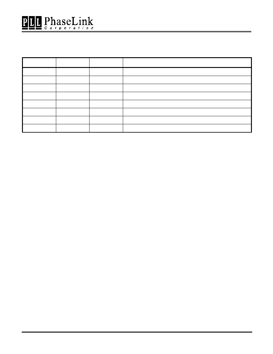
2. BYTE 7: Outputs Register (1=Enable, 0=Disable)
Bit
Pin#
Default
Description
Bit 7
30, 29
1
DDR7T, DDR7C
Bit 6
28, 27
1
DDR6T, DDR6C
Bit 5
21, 22
1
DDR5T, DDR5C
Bit 4
19, 20
1
DDR4T, DDR4C
Bit 3
15, 16
1
DDR3T, DDR3C
Bit 2
10, 11
1
DDR2T, DDR2C
Bit 1
6, 7
1
DDR1T, DDR1C
Bit 0
4, 5
1
DDR0T, DDR0C
PLL103-02 Rev.D
DDR SDRAM Buffer for Desktop PCs with 4 DDR DIMMS
47745 Fremont Blvd., Fremont, California 94538 TEL (510) 492-0990 FAX (510) 492-0991 Rev 01/11/01 Page 5
ELECTRICAL SPECIFICATIONS
1. Absolute Maximum Ratings
PARAMETERS
SYMBOL
MIN.
MAX.
UNITS
Supply Voltage
V
DD
V
SS
-
0.5
7.0
V
Input Voltage, dc
V
I
V
SS
-
0.5
V
DD
+
0.5
V
Output Voltage, dc
V
O
V
SS
-
0.5
V
DD
+
0.5
V
Storage Temperature
T
S
-65
150
∞
C
Ambient Operating Temperature
T
A
0
70
∞
C
ESD Voltage
2
KV
Exposure of the device under conditions beyond the limits specified by Maximum Ratings for extended periods may cause permanent damage to the
device and affect product reliability. These conditions represent a stress rating only, and functional operations of the device at these or any other
conditions above the operational limits noted in this specification is not implied.
2. Operating Conditions
PARAMETERS
SYMBOL
MIN.
MAX.
UNITS
Supply Voltage
V
DD2.5
2.375
2.625
V
Input Capacitance
C
IN
5
pF
Output Capacitance
C
OUT
6
pF
3. Electrical Specifications
PARAMETERS
SYMBOL
CONDITIONS
MIN.
TYP.
MAX.
UNITS
Input High Voltage
V
IH
All Inputs except I2C
2.0
V
DD
+0.3
V
Input Low Voltage
V
IL
All inputs except I2C
V
SS
-0.3
0.8
V
Input High Current
I
IH
V
IN
= V
DD
TBM
uA
Input Low Current
I
IL
V
IN
= 0
TBM
uA
Output High
Voltage
V
OH
IOL = -12mA, VDD = 2.375V
1.7
V
Output Low
Voltage
V
OL
IOL = 12mA, VDD = 2.375V
0.6
V
Output High
Current
I
OH
VDD = 2.375V, VOUT=1V
-18
-32
mA
Output Low
Current
I
OL
VDD = 2.375V, VOUT=1.2V
26
35
mA
Note: TBM: To be measured