
PLL103-11
Low Skew Buffers
47745 Fremont Blvd., Fremont, California 94538 TEL (510) 492-0990 FAX (510) 492-0991 Rev 11/07/00 Page 1
FEATURES
∑
Generates 13 copies of High-speed clock inputs.
∑
Supports up to three SDRAM DIMMS synchronous
clocks.
∑
Supports 2-wire I2C serial bus interface with
readback.
∑
50% duty cycle with low jitter.
∑
Less than 5ns delay.
∑
Skew between any outputs is less than 250 ps.
∑
Tri-state pin for testing.
∑
Frequency up to 150 MHz.
∑
3.0V-3.7V Supply range.
∑
Available in 28-pin 300mil SOIC package.
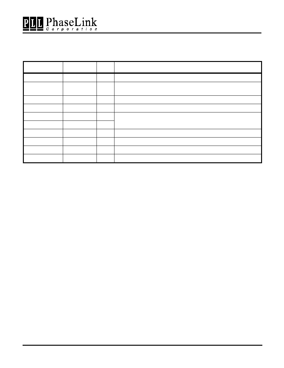
BLOCK DIAGRAM
PIN CONFIGURATION
POWER GROUP
∑
VDD: SDRAM (0:12)
∑
VDD1: I2C Circuitry
GROUND GROUP
∑
GND: SDRAM (0:12)
∑
GND1: I2C Circuitry
KEY SPECIFICATIONS
∑
BUF_IN to SDRAM outputs Delay: 1 ~ 5 ns.
∑
Output Slew:
1.5 V/ns.
∑
Output Skew:
±
250 ps.
∑
Output Duty Cycle: 50%
±
5%.
PLL103-11
28
26
25
24
23
1
2
3
4
5
6
7
8
9
10
11
12
VDD1
VDD
SDRAM0
VDD
13
14
SDATA
SDRAM1
GND
SDRAM2
SDRAM3
GND
BUF_IN
SDRAM4
SDRAM5
SDRAM12
27
22
21
20
19
18
17
16
15
GND1
VDD
SDRAM11
VDD
SCLK
SDRAM10
GND
SDRAM9
SDRAM8
GND
VDD
SDRAM7
SDRAM6
GND
BUF_IN
SDATA
SCLK
I2C
Control
SDRAM0
SDRAM1
SDRAM2
SDRAM3
SDRAM4
SDRAM5
SDRAM6
SDRAM7
SDRAM8
SDRAM9
SDRAM10
SDRAM11
SDRAM12
PLL103-11
Low Skew Buffers
47745 Fremont Blvd., Fremont, California 94538 TEL (510) 492-0990 FAX (510) 492-0991 Rev 11/07/00 Page 2
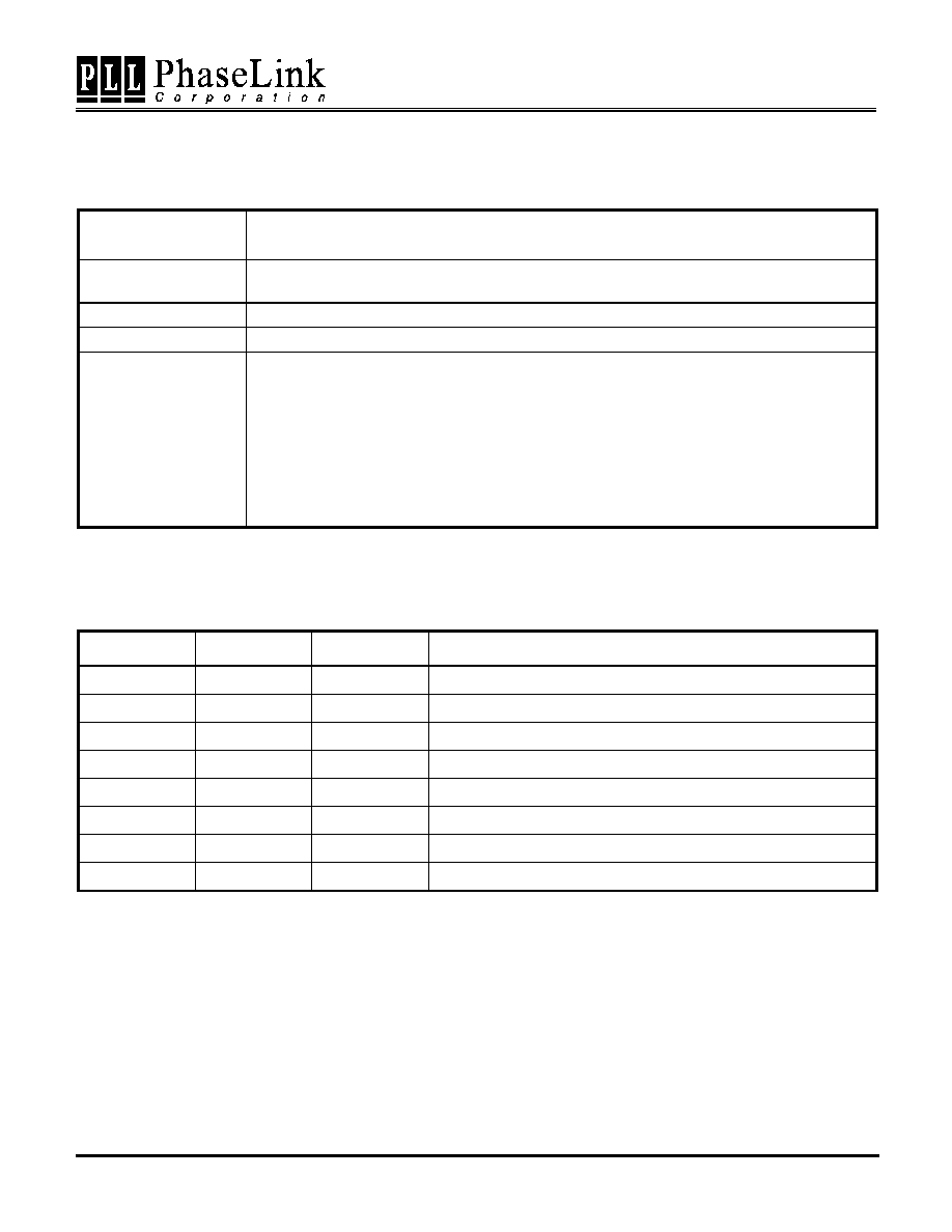
PIN DESCRIPTIONS
Name
Number
Type
Description
SDRAM (0:5)
2,3,6,7,10,11
O
SDRAM Byte0 Clock outputs.
SDRAM (6:11)
18,19,22,
23,26,27
O
SDRAM Byte1 Clock outputs.
SDRAM 12
12
O
SDRAM Byte2 Clock outputs.
BUF_IN
9
I
Input for fanout buffers SDRAM (0:12).
SDATA
14
B
SCLK
15
I
Serial data inputs for serial interface port.
VDD
1,5,20,24,28
P
3.3V Power supply for SDRAM buffer.
VDD1
13
P
3.3V Power supply for I2C circuitry.
GND
4,8,17,21,25
P
Ground for SDRAM buffer.
GND1
16
P
Power supply for I2C circuitry.
PLL103-11
Low Skew Buffers
47745 Fremont Blvd., Fremont, California 94538 TEL (510) 492-0990 FAX (510) 492-0991 Rev 11/07/00 Page 3
I2C BUS CONFIGURATION SETTING
Address Assignment
A6 A5 A4 A3 A2 A1 A0 R/W
1 1 0 1 0 0 1 _
Slave
Receiver/Transmitter
Provides both slave write and readback functionality
Data Transfer Rate
Standard mode at 100kbits/s
Data Protocol
This serial protocol is designed to allow both blocks write and read from the controller. The
bytes must be accessed in sequential order from lowest to highest byte. Each byte transferred
must be followed by 1 acknowledge bit. A byte transferred without acknowledged bit will
terminate the transfer. The write or read block both begins with the master sending a slave
address and a write condition (0xD2) or a read condition (0xD3).
Following the acknowledge of this address byte, in
Write Mode: the Command Byte and Byte
Count Byte must be sent by the master but ignored by the slave, in Read Mode: the Byte
Count Byte will be read by the master then all other Data Byte. Byte Count Byte default at
power-up is = (0x09).
I2C CONTROL REGISTERS
1. BYTE 0: SDRAM(0:5) Clock Register (1=Enable, 0=Disable)
Bit
Pin#
Default
Description
Bit 7
11
1
SDRAM5 (Active/Inactive)
Bit 6
10
1
SDRAM4 (Active/Inactive)
Bit 5
-
1
Reserved
Bit 4
-
1
Reserved
Bit 3
7
1
SDRAM3 (Active/Inactive)
Bit 2
6
1
SDRAM2 (Active/Inactive)
Bit 1
3
1
SDRAM1 (Active/Inactive)
Bit 0
2
1
SDRAM0 (Active/Inactive)

PLL103-11
Low Skew Buffers
47745 Fremont Blvd., Fremont, California 94538 TEL (510) 492-0990 FAX (510) 492-0991 Rev 11/07/00 Page 4
2. BYTE 1: SDRAM(6:11) Clock Register (1=Enable, 0=Disable)
Bit
Pin#
Default
Description
Bit 7
27
1
SDRAM11 (Active/Inactive)
Bit 6
26
1
SDRAM10 (Active/Inactive)
Bit 5
23
1
SDRAM9 (Active/Inactive)
Bit 4
22
1
SDRAM8 (Active/Inactive)
Bit 3
-
1
Reserved
Bit 2
-
1
Reserved
Bit 1
19
1
SDRAM7 (Active/Inactive)
Bit 0
18
1
SDRAM6 (Active/Inactive)
3. BYTE 2: SDRAM12 Clock Register (1=Enable, 0=Disable)
Bit
Pin#
Default
Description
Bit 7
-
1
Reserved
Bit 6
12
1
SDRAM12 (Active/Inactive)
Bit 5
-
1
Reserved
Bit 4
-
1
Reserved
Bit 3
-
1
Reserved
Bit 2
-
1
Reserved
Bit 1
-
1
Reserved
Bit 0
-
1
Reserved

PLL103-11
Low Skew Buffers
47745 Fremont Blvd., Fremont, California 94538 TEL (510) 492-0990 FAX (510) 492-0991 Rev 11/07/00 Page 5
ELECTRICAL SPECIFICATIONS
1. Absolute Maximum Ratings
PARAMETERS
SYMBOL
MIN.
MAX.
UNITS
Supply Voltage
V
DD
V
SS
-
0.5
7.0
V
Input Voltage, dc
V
I
V
SS
-
0.5
V
DD
+
0.5
V
Output Voltage, dc
V
O
V
SS
-
0.5
V
DD
+
0.5
V
Storage Temperature
T
S
-65
150
∞
C
Ambient Operating Temperature
T
A
0
70
∞
C
Exposure of the device under conditions beyond the limits specified by Maximum Ratings for extended periods may cause permanent damage to the
device and affect product reliability. These conditions represent a stress rating only, and functional operations of the device at these or any other
conditions above the operational limits noted in this specification is not implied.
2. AC/DC Electrical Specifications
PARAMETERS
SYMBOL
CONDITIONS
MIN.
TYP.
MAX.
UNITS
Input High Current
I
IH
V
IN
= V
DD
5
uA
I
IL
V
IN
=0V; with no pull-up resistors
uA
Input Low Current
I
IL
V
IN
=0V; with 100k pull-up resistors
uA
Input High Voltage
V
IH
2
V
DD
+
0.3
V
Input Low Voltage
V
IL
V
SS
-
0.3
0.8
V
Input Frequency
F
IN
V
DD
=3.3V; All outputs loaded
10
150
MHz
Input Capacitance
C
IN
Logic Inputs
5
pF
I
DD1
C
L
= 0pf @ 66MHz
80
120
mA
I
DD2
C
L
= 0pf @ 100MHz
120
180
mA
I
DD3
C
L
= 30pf; RS= 33
@ 66MHz
180
260
mA
I
DD4
C
L
= 30pf; RS= 33
@ 100MHz
240
360
mA
Operating Supply
Current
I
DD5
Stopped, input at 0 or VDD
500
uA

PLL103-11
Low Skew Buffers
47745 Fremont Blvd., Fremont, California 94538 TEL (510) 492-0990 FAX (510) 492-0991 Rev 11/07/00 Page 6
2. Output Buffer Electrical Specifications
Unless otherwise stated, all power supplies = 3.3V
±
5%, and ambient temperature range T
A
= 0
∞
C to 70
∞
C
PARAMETERS
SYMBOL
CONDITIONS
MIN.
TYP.
MAX.
UNITS
Output High Voltage
V
OH
I
OH
=
-
36 mA
2.4
3
V
Output Low Voltage
V
OL
I
OH
= 23 mA
0.27
0.4
V
Output High Current
I
OH
V
OH
= 2.0 V
-115
-54
mA
Output Low Current
I
OL
V
OL
= 0.8 V
40
57
mA
Output Impedance
R
DSP
V
O
= (0.5)
V
DD
10
24
ohm
Output Impedance
R
DSN
V
O
= (0.5)
V
DD
10
24
ohm
Rise Time
T
r
V
OL
= 0.4 V, V
OH
= 2.4V
0.95
1.33
ns
Fall Time
T
f
V
OH
= 2.4 V, V
OL
= 0.4V
0.95
1.33
ns
Skew
T
skew
V
T
= 1.5 V
110
250
ps
Duty Cycle
D
T
V
T
= 1.5 V
45
50
55
%
T
PROP
V
T
= 1.5 V
1
5
6
ns
T
PROPEN
V
T
= 1.5 V
1
8
ns
Propagation
T
PROPDIS
V
T
= 1.5 V
1
8
ns

PLL103-11
Low Skew Buffers
47745 Fremont Blvd., Fremont, California 94538 TEL (510) 492-0990 FAX (510) 492-0991 Rev 11/07/00 Page 7
PACKAGE INFORMATION
ORDERING INFORMATION
PhaseLink Corporation, reserves the right to make changes in its products or specifications, or both at any time without notice. The information
furnished by PhaseLink is believed to be accurate and reliable. However, PhaseLink makes no guarantee or warranty concerning the accuracy of said
information and shall not be responsible for any loss or damage of whatever nature resulting from the use of, or reliance upon this product.
LIFE SUPPORT POLICY: PhaseLink's products are not authorized for use as critical components in life support devices or systems without the
express written approval of the President of PhaseLink Corporation.
For part ordering, please contact our Sales Department:
47745 Fremont Blvd., Fremont, CA 94538, USA
Tel: (510) 492-0990 Fax: (510) 492-0991
PART NUMBER
The order number for this device is a combination of the following:
Device number, Package type and Operating temperature range
PLL103-11 S C
PART NUMBER
TEMPERATURATURE
C=COMMERCIAL
M=MILITARY
I=INDUSTRAL
PACKAGE TYPE
S=SOIC
0.005 - 0.0115
(0.127 - 0.2921)
0.701 - 0.711
(17.81 - 18.06)
(0.229 - 0.305)
45
0
0.009 - 0.012
0.050
(1.27)
MIN
3
0
-6
0
0.015
(0.381)
0.088 - 0.096
(2.235 - 2.438)
0.097 - 0.104
(2.464 - 2.642)
0.050
1.27
0.400 - 0.410
10.160 - 10.414
0.292 - 0.299
7.417 - 7.959
0.014 - 0.019
0.356 - 0.483
28 PIN SOIC