PLL130-07
High Speed Translator Buffer to CMOS (Selectable Drive)
47745 Fremont Blvd., Fremont, California 94538 Tel (510) 492-0990 Fax (510) 492-0991 www.phaselink.com Rev 09/09/04 Page 1
FEATURES
∑ CMOS output
∑ Selectable Drive capability (15pF or 30pF
output load).
∑ Single AC coupled input (min. 100mV swing).
∑ Input range from DC to 200 MHz.
∑ 2.5V to 3.3V operation.
∑ Available in 8-Pin SOIC and 3x3mm QFN.
DESCRIPTION
The PLL130-07 is a low cost, high performance,
high speed, buffer that reproduces any input fre-
quency from DC to 200MHz. It provides CMOS
output with 15pF output load drive capability.
Any input signal with at least 100mV swing can
be used as reference signal. This chip is ideal
for conversion from sine wave to CMOS.
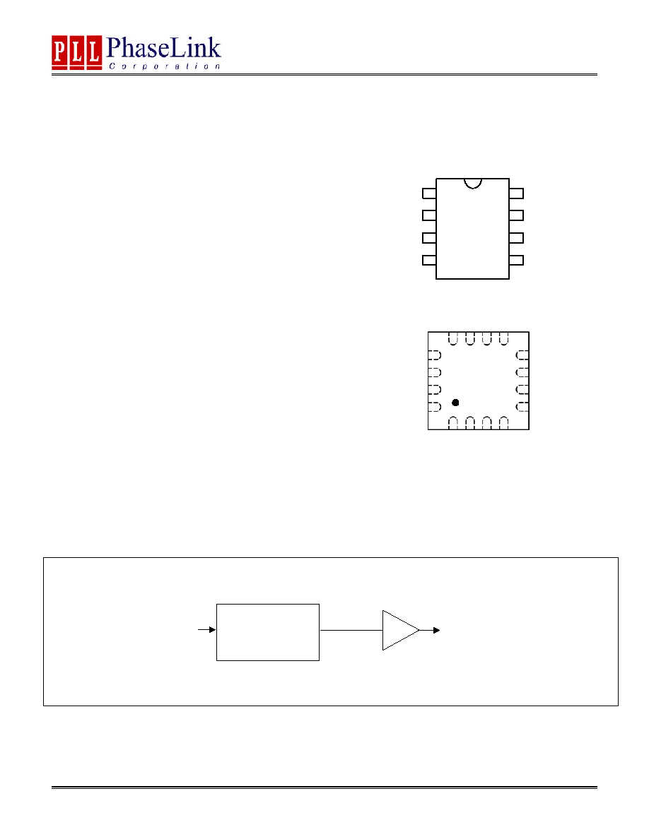
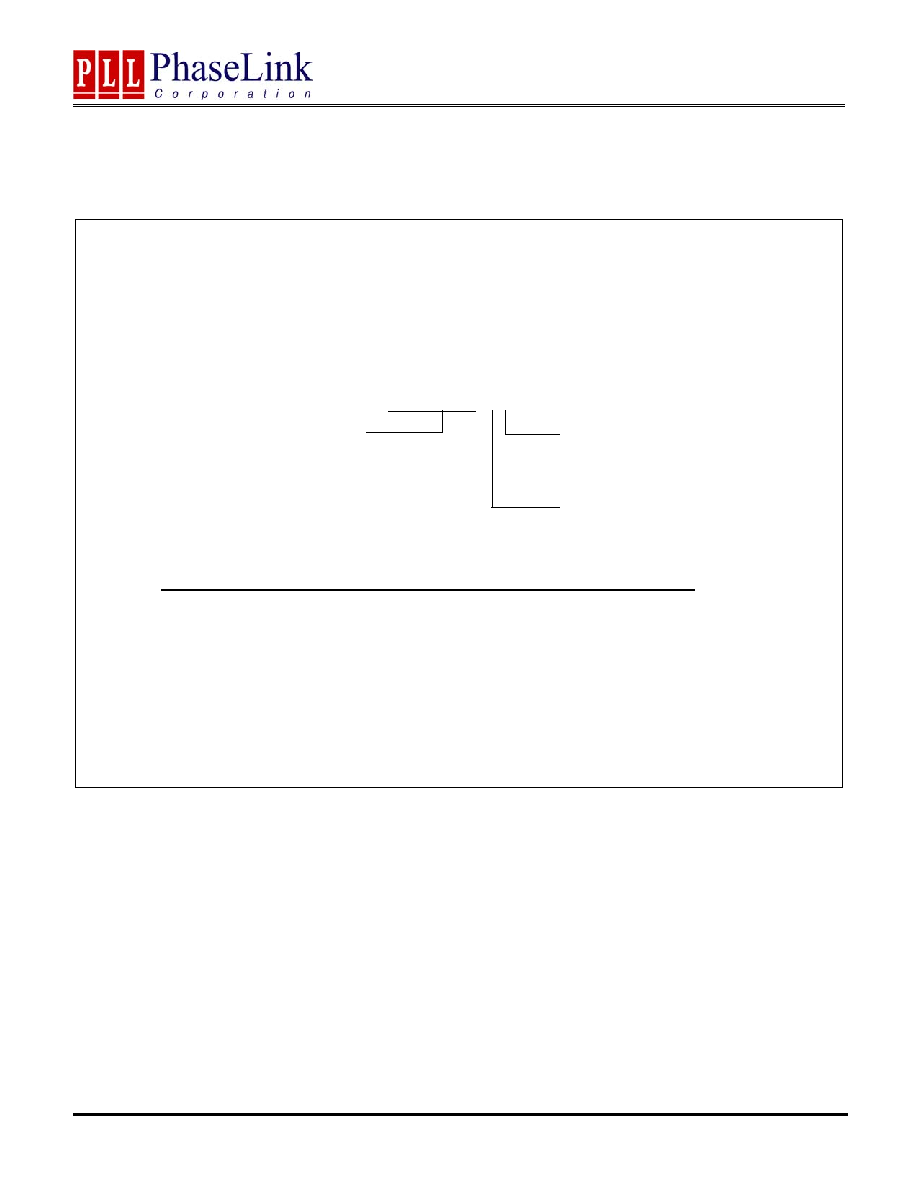
PIN CONFIGURATION
(TOP VIEW)
BLOCK DIAGRAM
Input
Amplifier
REF_IN
CLK_OUT
P
L
L
130-07
1
2
3
4
5
6
7
8
GND
REF_IN
GND
VDD
DRIV_SEL^
GND
CLK_OUT
VDD
PLL130-07
CLK_OUT
N/C
GND
VDD
1
2
3
4
12
11
10
9
13
14
15
16
8
7
6
5
VD
D
VD
D
GN
D
VD
D
GND
DRIV_SEL^
GND
OE^
GND
GND
REF_IN
GND
Note: ^ denotes internal pull up
PLL130-07
High Speed Translator Buffer to CMOS (Selectable Drive)
47745 Fremont Blvd., Fremont, California 94538 Tel (510) 492-0990 Fax (510) 492-0991 www.phaselink.com Rev 09/09/04 Page 2
PIN DESCRIPTION
Name
8pin SOIC
Pin number
3x3mm QFN
Pin number
Type Description
GND 1,3,6 1,2,4,5,
9,14,15
P Ground.
VDD 4,7 7,10,11,12
P
Power
supply.
DRIV_SEL 8
13
I
Drive Select input: `1' for standard drive, `0' for hi-drive output.
Internal pull-up (default is `1').
REF_IN 2
3 I
Reference input signal. The frequency of this signal will be
reproduced at the output (after translation to CMOS level).
CLK_OUT
5
8
O
CMOS clock output.
OE
N/A
16
I
Output enable (`1' for enable). Internal pull-up (default is `1').
ELECTRICAL SPECIFICATIONS
1. Absolute Maximum Ratings
PARAMETERS SYMBOL
MIN.
MAX.
UNITS
Supply Voltage
V
DD
4.6 V
Input Voltage, dc
V
I
-0.5
V
DD
+0.5 V
Output Voltage, dc
V
O
-0.5
V
DD
+0.5 V
Storage Temperature
T
S
-65 150
∞C
Ambient Operating Temperature*
T
A
-40 85
∞C
Junction Temperature
T
J
125
∞C
Lead Temperature (soldering, 10s)
260
∞C
ESD Protection, Human Body Model
2
kV
Exposure of the device under conditions beyond the limits specified by Maximum Ratings for extended periods may cause permanent damage to the
device and affect product reliability. These conditions represent a stress rating only, and functional operations of the device at these or any other con-
ditions above the operational limits noted in this specification is not implied.
* Note: Operating Temperature is guaranteed by design for all parts (COMMERCIAL and INDUSTRIAL), but tested for COMMERCIAL grade only.
2. AC Specifications
PARAMETERS CONDITIONS
MIN.
TYP.
MAX.
UNITS
Input Frequency
0
200
MHz
Input signal swing
REF_IN input
100
mV
Output Frequency
0
200
MHz
PLL130-07
High Speed Translator Buffer to CMOS (Selectable Drive)
47745 Fremont Blvd., Fremont, California 94538 Tel (510) 492-0990 Fax (510) 492-0991 www.phaselink.com Rev 09/09/04 Page 3
3. CMOS Output Electrical Specifications
PARAMETERS SYMBOL CONDITIONS MIN.
TYP.
MAX.
UNITS
Output High Voltage
V
OH
I
OH
= -12mA
2.4
V
Output Low Voltage
V
OL
I
LO
= 12mA
0.4
V
Output High Voltage at CMOS
level
V
OHC
I
OH
= -4mA
V
DD
≠ 0.4
V
At TTL level (High drive*)
36
51
mA
Output drive current
At TTL level (Standard drive)
12
17
mA
* Note: High Drive CMOS is selectable through DRIV_SEL selector input on pin 8(SOIC) or 13(QFN).
4. CMOS Switching Characteristics
PARAMETERS SYMBOL CONDITIONS MIN.
TYP.
MAX.
UNITS
0.8V ~ 2.0V with 10 pF load
1.15
Output Clock Rise/Fall Time
0.3V ~ 3.0V with 15 pF load
3.7
0.8V ~ 2.0V with 10 pF load
0.5
Output Clock Rise/Fall Time
(High Drive*)
0.3V ~ 3.0V with 15 pF load
1.5
ns
* Note: High Drive CMOS is selectable through DRIV_SEL selector input on pin 8(SOIC) or 13(QFN).
PLL130-07
High Speed Translator Buffer to CMOS (Selectable Drive)
47745 Fremont Blvd., Fremont, California 94538 Tel (510) 492-0990 Fax (510) 492-0991 www.phaselink.com Rev 09/09/04 Page 4
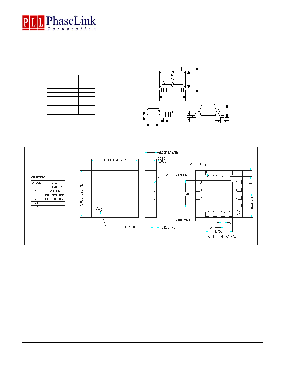
PACKAGE INFORMATION
C
L
A
8 PIN ( dimensions in mm )
Narrow SOIC
Symbol
Min.
Max.
A
1.47
1.73
A1
0.10
0.25
B
0.33
0.51
C
0.19
0.25
D
4.80
4.95
E
3.80
4.00
H
5.80
6.20
L
0.38
1.27
e
1.27 BSC
E
H
D
A
1
e
B
PLL130-07
High Speed Translator Buffer to CMOS (Selectable Drive)
47745 Fremont Blvd., Fremont, California 94538 Tel (510) 492-0990 Fax (510) 492-0991 www.phaselink.com Rev 09/09/04 Page 5
ORDERING INFORMATION
PhaseLink Corporation, reserves the right to make changes in its products or specifications, or both at any time without notice. The information fur-
nished by Phaselink is believed to be accurate and reliable. However, PhaseLink makes no guarantee or warranty concerning the accuracy of said
information and shall not be responsible for any loss or damage of whatever nature resulting from the use of, or reliance upon this product.
LIFE SUPPORT POLICY: PhaseLink's products are not authorized for use as critical components in life support devices or systems without the ex-
press written approval of the President of PhaseLink Corporation.
For part ordering, please contact our Sales Department:
47745 Fremont Blvd., Fremont, CA 94538, USA
Tel: (510) 492-0990 Fax: (510) 492-0991
PART NUMBER
The order number for this device is a combination of the following:
Device number, Package type and Operating temperature range
PLL130-07 x C
Order Number
Marking
Package Option
PLL130-07QC-R P130-07QC QFN - Tape and Reel
PLL130-07QC
P130-07QC
QFN - Tube
PLL130-07SC-R P130-07SC SOIC -Tape and Reel
PLL130-07SC P130-07SC SOIC
-
Tube
PART NUMBER
TEMPERATURE
C=COMMERCIAL
I=INDUSTRAL
PACKAGE TYPE
S=SOIC; Q=QFN