 | –≠–ª–µ–∫—Ç—Ä–æ–Ω–Ω—ã–π –∫–æ–º–ø–æ–Ω–µ–Ω—Ç: PLL202-02 | –°–∫–∞—á–∞—Ç—å:  PDF PDF  ZIP ZIP |

Preliminary
PLL202-02
System Clock Generator for various SOC
47745 Fremont Blvd., Fremont, California 94538 TEL (510) 492-0990 FAX (510) 492-0991 Rev 12/04/02 Page 1
FEATURES
∑ Generates all clock frequencies for multiple CPU
clocks and various SOC.
∑ Support one CPU clock.
∑ One 24MHz clock and one 48MHz clock.
∑ One 14.318MHz reference clocks.
∑ 3.3V operation; 50% percent duty cycle.
∑ Available in 14-pin 300mil DIP.
BLOCK DIAGRAM
PIN CONFIGURATION
Note:
^: Pull up, v :Pull down
*
: Bi-directional latched at power-up
PL
L
2
0
2
-
0
2
14
12
11
10
9
1
2
3
4
5
6
7
GND
XIN
GND
XOUT
VDD
GND
13
8
VDD
VDD
GND
CP U
VDD
24MHz/FS 1*^
48MHz/FS 0*^
REF/FS 2*^
Co n tro l
Lo g ic
VDD
REF
FS (0:2)*
P LL1
S S T
24Mh z
VDD
48Mh z
P LL2
VDD
C P U_F
XIN
XO UT
XTAL
OS C

Preliminary
PLL202-02
System Clock Generator for various SOC
47745 Fremont Blvd., Fremont, California 94538 TEL (510) 492-0990 FAX (510) 492-0991 Rev 12/04/02 Page 2
PIN DESCRIPTIONS
Name Number
Type
Description
GND 1,5,6,12
P
Ground.
XIN
2
I
14.318MHz crystal input to be connected to one end of the crystal.
XOUT
3
O
14.318MHz crystal output.
REF/F2*
24MHz/F1*
48MHz/F0*
7,8,13 B
At power up, these pins are input pins and will determine the CPU clock
frequency. After input sampling, these pins will generate output clocks.
FS0, FS1 and FS2 have internal pull up (high by default).
24MHz
7
B
24MHz output for SUPER I/O after input data latched during power-on.
48MHz
8
B
48MHz output for USB after input data latched during power-on.
VDD
4,9,10,14
P
3.3V Power supply.
CPU
11
O
CPU clocks with frequencies defined by Frequency Table.
FREQUENCY (MHz) SELECTION TABLE
FS2 FS1 FS0
CPU
0 0 0
80
0 0 1
75
0 1 0
83.3
0 1 1
66.8
1 0 0
103
1 0 1
112
1 1 0
68
1 1 1
100.2

Preliminary
PLL202-02
System Clock Generator for various SOC
47745 Fremont Blvd., Fremont, California 94538 TEL (510) 492-0990 FAX (510) 492-0991 Rev 12/04/02 Page 3
ELECTRICAL SPECIFICATIONS
1. Absolute Maximum Ratings
PARAMETERS SYMBOL
MIN.
MAX.
UNITS
Supply Voltage
V
DD
V
SS
-
0.5
7 V
Input Voltage, dc
V
I
V
SS
-
0.5 V
DD
+
0.5
V
Output Voltage, dc
V
O
V
SS
-
0.5 V
DD
+
0.5
V
Storage Temperature
T
S
-65 150
∞C
Ambient Operating Temperature
T
A
0 70
∞C
Junction Temperature
T
J
115
∞C
ESD Voltage
2
KV
Exposure of the device under conditions beyond the limits specified by Maximum Ratings for extended periods may cause permanent damage to the
device and affect product reliability. These conditions represent a stress rating only, and functional operations of the device at these or any other
conditions above the operational limits noted in this specification is not implied.
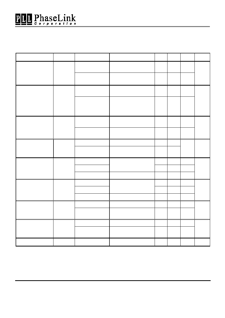
2. AC/DC Electrical Specifications
PARAMETERS SYMBOL
CONDITIONS
MIN.
TYP.
MAX.
UNITS
Input High Voltage
V
IH
All Inputs except XIN
2
V
DD
+0.3 V
Input Low Voltage
V
IL
All inputs except XIN
V
SS
-0.3 0.8 V
Input High Current
I
IH
V
IN
= V
DD
5
uA
Input Low Current
I
IL1
VIN = 0V; Inputs with
no pull-up resistors
-5 uA
Input Low Current
I
IL2
VIN = 0V; Inputs with
pull-up resistors
-200 uA
Pull-up resistor
R
Pu
Pin
7,8,13
240
Kohm
Input frequency
F
I
V
DD
= 3.3V
12
14.318
16
Mhz
C
IN
Logic Inputs
5
PF
Input Capacitance
C
INX
XIN & XOUT pins
27
36
45
PF
Preliminary
PLL202-02
System Clock Generator for various SOC
47745 Fremont Blvd., Fremont, California 94538 TEL (510) 492-0990 FAX (510) 492-0991 Rev 12/04/02 Page 4
3. Output Buffer Electrical Specifications
Unless otherwise stated, all power supplies = 3.3V
±5%, and ambient temperature range T
A
= 0
∞C to 70∞C
PARAMETERS SYMBOL OUTPUTS
CONDITIONS MIN.
TYP.
MAX.
UNITS
CPU
Measured @ 0.4V ~ 2.0V,
C
L
=10-20pf
1 4
Output Rise time
T
OR
REF, 48MHz,
24MHz
Measured @ 0.4V ~ 2.4V,
C
L
=10-30pf
1 4
V/ns
CPU
Measured @ 2.0 ~ 0.4V,
C
L
=10-20pf
1 4
Output Fall time
T
OF
REF, 48MHz,
24MHz
Measured @ 2.4V ~ 0.4V,
C
L
=10-30pf
1 4
V/ns
CPU, 48MHz,
24MHz
Measured @ 1.5V
C
L
=20pf
45 50 55
Duty Cycle
D
T
REF
Measured @ 1.5V,
C
L
=20~30pf
40 60
%
CPU
V
DD
=3.3V
±5%
30
Output Impedance
Z
0
REF, 48MHz,
24MHz
V
DD
=3.3V
±5%
25
Ohm
REF 40
50
65
48MHz, 24MHz
V
OL
= 1.5V
40 50 65
Output High Current
I
OH
CPU
V
OH
= 1.5
45 60 80
mA
REF 40
50
65
48MHz, 24MHz
V
OL
= 1.5V
40 50 65
Output Low Current
I
OL
CPU
V
OL
= 1.5V
45 60 80
mA
CPU
Measured @ 1.5V
150
Jitter, One Sigma
J
sigma
REF, 48MHz,
24MHz
Measured @ 1.5V
500
ps
CPU
Measured @ 1.5V
-0.25 0.25
Jitter, Absolute
J
Abs
REF, 48MHz,
24MHz
Measured @ 1.5
-1 1
ns
Jitter(cycle to cycle)
J
cyc-cyc
CPU
Measured @ 1.5V
250
ps

Preliminary
PLL202-02
System Clock Generator for various SOC
47745 Fremont Blvd., Fremont, California 94538 TEL (510) 492-0990 FAX (510) 492-0991 Rev 12/04/02 Page 5
PACKAGE INFORMATION
ORDERING INFORMATION
PhaseLink Corporation, reserves the right to make changes in its products or specifications, or both at any time without notice. The information
furnished by PhaseLink is believed to be accurate and reliable. However, PhaseLink makes no guarantee or warranty concerning the accuracy of said
information and shall not be responsible for any loss or damage of whatever nature resulting from the use of, or reliance upon this product.
LIFE SUPPORT POLICY: PhaseLink's products are not authorized for use as critical components in life support devices or systems without the
express written approval of the President of PhaseLink Corporation.
For part ordering, please contact our Sales Department:
47745 Fremont Blvd., Fremont, CA 94538, USA
Tel: (510) 492-0990 Fax: (510) 492-0991
PART NUMBER
The order number for this device is a combination of the following:
Device number, Package type and Operating temperature range
PLL202-02 PC
14 P IN DIP
TEMPERATURATURE
C=COMMERCIAL
M=MILITARY
I=INDUSTRAL
PART NUMBER
PACKAGE TYPE
P=DIP